

Page 1
Octal 8-Bit TrimDAC
DAC 8
V
OUT
V
REFH
V
REFL
.
.
.
.
.
.
AD8801/AD8803
V
REFL
V
REFH
O1
O8
SHDNRS
CS
CLK
SDI
GND
V
DD
8
8
8
88
8
3
DAC
SELECT
11-BIT
SERIAL
LATCH
D
CK
RS
1
8
ADDRESS
8-BIT
LATCH
CK
RS
8-BIT
LATCH
CK RS
DAC 1
V
OUT
V
REFH
V
REFL
a
FEATURES
Low Cost
Replaces Eight Potentiometers
Eight Individually Programmable Outputs
Three-Wire Serial Input
Power Shutdown ≤ 25 mW Including I
Midscale Preset, AD8801
Separate V
Range Setting, AD8803
REFL
+3 V to +5 V Single Supply Operation
APPLICATIONS
Automatic Adjustment
Trimmer Potentiometer Replacement
Video and Audio Equipment Gain and Offset Adjustment
Portable and Battery Operated Equipment
GENERAL DESCRIPTION
The AD8801/AD8803 provides eight digitally controlled dc
voltage outputs. This potentiometer divider TrimDAC
replacement of the mechanical trimmer function in new designs.
The AD8801/AD8803 is ideal for dc voltage adjustment
applications.
Easily programmed by serial interfaced microcontroller ports,
the AD8801 with its midscale preset is ideal for potentiometer
replacement where adjustments start at a nominal value. Applications such as gain control of video amplifiers, voltage controlled frequencies and bandwidths in video equipment,
geometric correction and automatic adjustment in CRT computer graphic displays are a few of the many applications ideally
suited for these parts. The AD8803 provides independent control of both the top and bottom end of the potentiometer divider
allowing a separate zero-scale voltage setting determined by the
V
pin. This is helpful for maximizing the resolution of de-
REFL
vices with a limited allowable voltage control range.
See the AD8802/AD8804 for a twelve channel version of this product.
TrimDAC is a registered trademark of Analog Devices, Inc.
REV. A
Information furnished by Analog Devices is believed to be accurate and
reliable. However, no responsibility is assumed by Analog Devices for its
use, nor for any infringements of patents or other rights of third parties
which may result from its use. No license is granted by implication or
otherwise under any patent or patent rights of Analog Devices.
DD
and I
REF
®
allows
with Power Shutdown
AD8801/AD8803
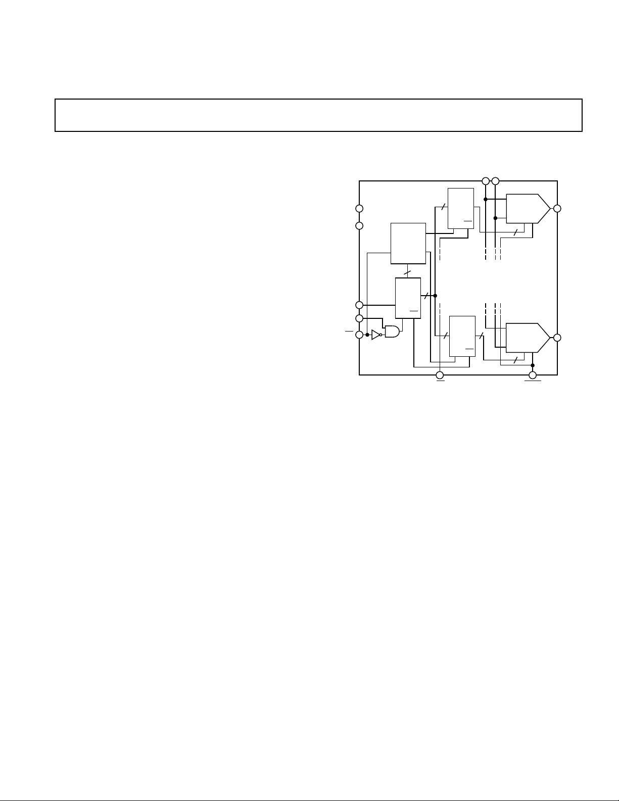
FUNCTIONAL BLOCK DIAGRAM
(DACs 2–7 Omitted for Clarity)
Internally the AD8801/AD8803 contain eight voltage output
digital-to-analog converters, sharing a common reference voltage input.
Each DAC has its own DAC register that holds its output state.
These DAC registers are updated from an internal serial-to-parallel shift register that is loaded from a standard three-wire serial
input digital interface. Eleven data bits make up the data word
clocked into the serial input register. This data word is decoded
where the first 3 bits determine the address of the DAC register
to be loaded with the last 8 bits of data. The AD8801/AD8803
consumes only 5 µA from 5 V power supplies. In addition, in
shutdown mode reference input current consumption is also reduced to 5 µA while saving the DAC latch settings for use after
return to normal operation.
The AD8801/AD8803 is available in 16-pin plastic DIP and the
1.5 mm height SO-16 surface mount packages.
© Analog Devices, Inc., 1995
One Technology Way, P.O. Box 9106, Norwood. MA 02062-9106, U.S.A.
Tel: 617/329-4700 Fax: 617/326-8703
Page 2

AD8801/AD8803–SPECIFICATIONS
(VDD = +3 V 6 10% or +5 V 6 10%, V
≤ TA ≤ +858C unless otherwise noted)
= +VDD, V
REFH
= 0 V, –408C
REFL
Parameter Symbol Conditions Min Typ1Max Units
STATIC ACCURACY
Specifications Apply to All DACs
Resolution N 8 Bits
Integral Nonlinearity Error INL –1.5 ±1/2 +1.5 LSB
Differential Nonlinearity DNL Guaranteed Monotonic –1 ±1/4 +1 LSB
Full-Scale Error G
Zero-Code Error V
DAC Output Resistance R
Output Resistance Match ∆R/R
REFERENCE INPUT
Voltage Range
Input Resistance R
Reference Input Capacitance
2
3
V
V
C
C
FSE
ZSE
OUT
REFH
REFL
REFH
REF0
REF1
O
Pin Available on AD8803 Only 0 V
Digital Inputs = 55H, V
REFH
= V
DD
Digital Inputs All Zeros 25 pF
Digital Inputs All Ones 25 pF
–4 –2.8 +0.5 LSB
–0.5 ±0.1 +0.5 LSB
358 kΩ
1%
0V
DD
DD
V
V
2kΩ
DIGITAL INPUTS
Logic High V
Logic Low V
Logic High V
Logic Low V
Input Current I
Input Capacitance
POWER SUPPLIES
3
4
Power Supply Range V
Supply Current (CMOS) I
Supply Current (TTL) I
Shutdown Current I
Power Dissipation P
IH
IL
IH
IL
IL
C
IL
Range 2.7 5.5 V
DD
DD
DD
REFH
DISS
Power Supply Sensitivity PSRR V
Power Supply Sensitivity PSRR VDD = 3 V ± 10%, V
DYNAMIC PERFORMANCE
V
Settling Time (Positive or Negative) t
OUT
3
S
VDD = +5 V 2.4 V
VDD = +5 V 0.8 V
VDD = +3 V 2.1 V
VDD = +3 V 0.6 V
VIN = 0 V or +5 V ±1 µA
5pF
VIH = VDD or VIL = 0 V 0.01 5 µA
VIH = 2.4 V or VIL = 0.8 V, VDD= +5.5 V 1 4 mA
SHDN = 0 0.01 5 µA
VIH = VDD or VIL = 0 V, VDD = +5.5 V 27.5 µW
= 5 V ± 10%, V
DD
= +4.5 V 0.001 0.002 %/%
REFH
= +2.7 V 0.01 %/%
REFH
±1/2 LSB Error Band 0.6 µs
Crosstalk CT See Note 5, f = 100 kHz 50 dB
SWITCHING CHARACTERISTICS
Input Clock Pulse Width tCH, t
Data Setup Time t
Data Hold Time t
CS Setup Time t
CS High Pulse Width t
Reset Pulse Width t
CLK Rise to
CS Rise Hold Time t
CS Rise to Next Rising Clock t
NOTES
1
Typical values represent average readings measured at +25 °C.
2
V
can be any value between GND and VDD, for the AD8803 V
REFH
3
Guaranteed by design and not subject to production test.
4
Digital Input voltages VIN = 0 V or VDD for CMOS condition. DAC outputs unloaded. P
5
Measured at a V
6
See timing diagram for location of measured values. All input control voltages are specified with tR = tF = 2 ns (10% to 90% of VDD) and timed from a voltage
level of 1.6 V.
Specifications subject to change without notice.
pin where an adjacent V
OUT
3, 6
CL
DS
DH
CSS
CSW
RS
CSH
CS1
pin is making a full-scale voltage change.
OUT
Clock Level High or Low 15 ns
can be any value between GND and VDD.
REFL
is calculated from (IDD × VDD).
DISS
5ns
5ns
10 ns
10 ns
60 ns
15 ns
10
ns
–2–
REV. A
Page 3
AD8801/AD8803
V
REFH
O1
V
DD
RS
O4
SHDN
CS
O6
O5
SDI
O2
O3
O8
O7
GND CLK
1
2
16
15
5
6
7
12
11
10
3
4
14
13
89
TOP VIEW
(Not to Scale)
AD8801
V
REFH
O1
V
DD
O8
O4
SHDN
CS
O5
SDI
CLK
O2
O3
O7
O6
GND V
REFL
1
2
16
15
5
6
7
12
11
10
3
4
14
13
89
TOP VIEW
(Not to Scale)
AD8803
WARNING!
ESD SENSITIVE DEVICE
ABSOLUTE MAXIMUM RATINGS
(TA = +25°C, unless otherwise noted)
VDD to GND . . . . . . . . . . . . . . . . . . . . . . . . . . . . . . –0.3, +8 V
V
to GND . . . . . . . . . . . . . . . . . . . . . . . . . . . . . . 0 V, V
REFX
Outputs (Ox) to GND . . . . . . . . . . . . . . . . . . . . . . . . 0 V, V
Digital Input Voltage to GND . . . . . . . . . . . . . . . . . . 0 V, V
DD
DD
DD
Operating Temperature Range . . . . . . . . . . . . .–40°C to +85°C
Maximum Junction Temperature (T
MAX) . . . . . . . . +150°C
J
Storage Temperature . . . . . . . . . . . . . . . . . . .–65°C to +150°C
Lead Temperature (Soldering, 10 sec) . . . . . . . . . . . . . +300°C
Package Power Dissipation . . . . . . . . . . . . .(T
Thermal Resistance θ
JA,
MAX – TA)/θ
J
JA
SOIC (SO-16) . . . . . . . . . . . . . . . . . . . . . . . . . . . . . 60°C/W
P-DIP (N-16) . . . . . . . . . . . . . . . . . . . . . . . . . . . . . . 57°C/W
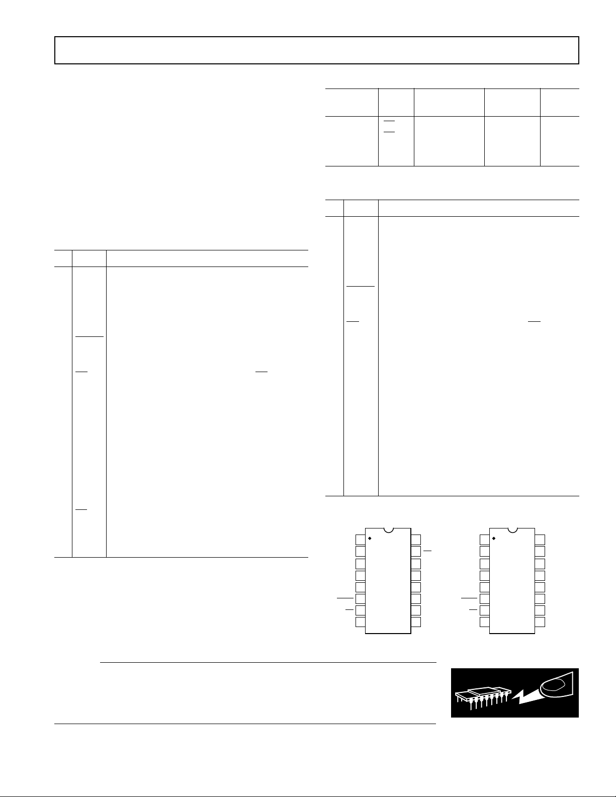
AD8801 PIN DESCRIPTIONS
Pin Name Description
1V
2 O1 DAC Output #1, Addr = 000
3 O2 DAC Output #2, Addr = 001
4 O3 DAC Output #3, Addr = 010
5 O4 DAC Output #4, Addr = 011
Common DAC Reference Input
REFH
2
2
2
2
6 SHDN Reference input open circuit, active low, all
DAC outputs open circuit. DAC latch settings
maintained.
7
CS Chip Select Input, active low. When CS returns
high, data in the serial input register is decoded
based on the address bits and loaded into the tar-
get DAC register.
8 GND Ground
9 CLK Serial Clock Input, Positive Edge Triggered
10 SDI Serial Data Input
11 O5 DAC Output #5, Addr = 100
12 O6 DAC Output #6, Addr = 101
13 O7 DAC Output #7, Addr = 110
14 O8 DAC Output #8, Addr = 111
2
2
2
2
15 RS Asynchronous preset to midscale output setting,
16 V
active low. Loads all DAC latches with 80
Positive power supply, specified for operation at
DD
.
H
both +3 V and +5 V.
ORDERING GUIDE
Package Package
Model FTN Temperature Description Option
AD8801AN
AD8801AR
RS –40°C to +85°C PDIP-16 N-16
RS –40°C to +85°C SO-16 R-16A
AD8803AN REFL –40°C to +85°C PDIP-16 N-16
AD8803AR REFL –40°C to +85°C SO-16 R-16A
AD8803 PIN DESCRIPTIONS
Pin Name Description
1V
2 O1 DAC Output #1, Addr = 000
3 O2 DAC Output #2, Addr = 001
4 O3 DAC Output #3, Addr = 010
5 O4 DAC Output #4, Addr = 011
Common High-Side DAC Reference Input
REFH
2
2
2
2
6 SHDN Reference inputs open circuit, active low, all
DAC outputs open circuit. DAC latch settings
maintained.
7
CS Chip Select Input, active low. When CS returns
high, data in the serial input register is decoded
based on the address bits and loaded into the tar-
get DAC register.
8 GND Ground
9V
Common Low-Side DAC Reference Input
REFL
10 CLK Serial Clock Input, Positive Edge Triggered
11 SDI Serial Data Input
12 O5 DAC Output #5, Addr = 100
13 O6 DAC Output #6, Addr = 101
14 O7 DAC Output #7, Addr = 110
15 O8 DAC Output #8, Addr = 111
16 V
Positive power supply, specified for operation at
DD
2
2
2
2
both +3 V and +5 V.
PIN CONFIGURATIONS
CAUTION
ESD (electrostatic discharge) sensitive device. Electrostatic charges as high as 4000 V readily
accumulate on the human body and test equipment and can discharge without detection.
Although these devices feature proprietary ESD protection circuitry, permanent damage may
occur on devices subjected to high energy electrostatic discharges. Therefore, proper ESD
REV. A
precautions are recommended to avoid performance degradation or loss of functionality.
–3–
Page 4
AD8801/AD8803
OCTAL 8-BIT TRIMDAC, WITH SHUTDOWN
1
V
SDI
CLK
CS
OUT
A2 A1 A0 D7 D6 D5 D4 D3 D2 D1 D0
0
1
0
1
0
+5V
0V
DAC REGISTER LOAD
Figure 2a. Timing Diagram
DETAIL SERIAL DATA INPUT TIMING (RS = "1")
SDI
1
(DATA
CLK
CS
V
OUT
AX OR D
0
IN)
1
0
t
CSS
1
0
+5V
0V
AX OR D
X
t
CH
X
t
DS
t
DH
t
t
CSH
CL
±1 LSB ERROR BAND
Figure 2b. Detail Timing Diagram
RESET TIMING
1
RS
0
+5V
V
OUT
2.5V
t
RS
t
S
±1 LSB ERROR BAND
following address assignments for the ADDR decode which determines the location of DAC register receiving the serial register data in bits B7 through B0:
DAC # = A2 × 4 + A1 × 2 + A0 + 1
DAC outputs can be changed one at a time in random sequence. The fast serial-data loading of 33 MHz makes it possible
to load all eight DACs in as little time as 3 µs (12 × 8 × 30 ns).
The exact timing requirements are shown in Figure 2.
The AD8801 offers a midscale preset activated by the
RS pin
simplifying initial setting conditions at first power up. The
AD8803 has both a V
REFH
and a V
pin to establish indepen-
REFL
dent positive full-scale and zero-scale settings to optimize resolution. Both parts offer a power shutdown
SHDN that places
the DAC structure in a zero power consumption state resulting
in only leakage currents being consumed from the power supply,
V
inputs, and all 8 outputs. In shutdown mode the DACx
t
CS1
REF
latch settings are maintained. When returning to operational
mode from power shutdown the DAC outputs return to their
previous voltage settings.
V
REFH
DAC
REGISTER
TO OTHER DACS
P CH
N CH
D7
D6
D0
.
.
.
.
.
.
MSB
O
2R
2R
X
R
R
.
.
.
t
CSW
t
S
±1 LSB
±1 LSB
Figure 2c. Reset Timing Diagram
Table I. Serial-Data Word Format
ADDR DATA
B10 B9 B8 B7 B6 B5 B4 B3 B2 B1 B0
A2 A1 A0 D7 D6 D5 D4 D3 D2 D1 D0
MSB LSB MSB LSB
2102928272625242322212
0
OPERATION
The AD8801/AD8803 provides eight channels of programmable
voltage output adjustment capability. Changing the programmed
output voltage of each TrimDAC is accomplished by clocking in
an 11-bit serial data word into the SDI (Serial Data Input) pin.
The format of this data word is three address bits, MSB first,
followed by eight data bits, MSB first. Table I provides the serial register data word format. The AD8801/AD8803 has the
2R
2R
V
GND
REFL
LSB
Figure 3. AD8801/AD8803 Equivalent TrimDAC Circuit
PROGRAMMING THE OUTPUT VOLTAGE
The output voltage range is determined by the external reference connected to V
REFH
and V
pins. See Figure 3 for a
REFL
simplified diagram of the equivalent DAC circuit. In the case of
the AD8801, its V
therefore cannot be offset. V
is internally connected to GND and
REFL
can be tied to VDD and V
REFH
REFL
can be tied to GND establishing a basic rail-to-rail voltage output programming range. Other output ranges are established by
the use of different external voltage references. The general
transfer equation that determines the programmed output
voltage is:
V
(Dx) = (Dx)/256 × (V
O
REFH
– V
REFL
) + V
REFL
(1)
where Dx is the data contained in the 8-bit DACx latch.
–4–
REV. A
Page 5
AD8801/AD8803
LOGIC
100Ω
For example, when V
= +5 V and V
REFH
= 0 V the follow-
REFL
ing output voltages will be generated for the following codes:
DVOXOutput State
(V
= +5 V, V
REFH
REFL
= 0 V)
255 4.98 V Full-Scale
128 2.50 V Half-Scale (Midscale Reset Value)
1 0.02 V 1 LSB
0 0.00 V Zero-Scale
REFERENCE INPUTS (V
REFH
, V
REFL
)
The reference input pins set the output voltage range of all eight
DACs. In the case of the AD8801 only the V
pin is avail-
REFH
able to establish a user designed full-scale output voltage. The
external reference voltage can be any value between 0 and V
DD
but must not exceed the VDD supply voltage. In the case of the
AD8803, which has access to the V
which establishes the
REFL
zero-scale output voltage, any voltage can be applied between
0 V and V
V
REFH
. V
DD
can be smaller or larger in voltage than
REFL
since the DAC design uses fully bidirectional switches as
shown in Figure 3. The input resistance to the DAC has a code
dependent variation that has a nominal worst case measured at
55
, which is approximately 2 kΩ. When V
H
V
, the REFL reference must be able to sink current out of
REFL
is greater than
REFH
the DAC ladder, while the REFH reference is sourcing current
into the DAC ladder. The DAC design minimizes reference
glitch current maintaining minimum interference between DAC
channels during code changes.
DAC OUTPUTS (O1–O8)
The eight DAC outputs present a constant output resistance of
approximately 5 kΩ independent of code setting. The distribution of R
from DAC to DAC typically matches within ±1%.
OUT
However, device to device matching is process lot dependent
having a ±20% variation. The change in R
with temperature
OUT
has a 500 ppm/°C temperature coefficient. During power shutdown all eight outputs are open circuited.
CS
CLK
SDI
D
D10
SER
REG
ADDR
D9
D8
D7
.
.
.
D0
8
EN
DEC
...
...
...
AD8801/AD8803
D7
DAC
REG
#1
D0
D7
DAC
REG
#8
D0
DAC
DAC
R
..
..
..
DAC
R
V
DD
V
REFH
1
8
O1
O2
O3
O4
O5
O6
O7
O8
DIGITAL INTERFACING
The AD8801/AD8803 contains a standard three-wire serial input control interface. The three inputs are clock (CLK),
CS and
serial data input (SDI). The positive-edge sensitive CLK input
requires clean transitions to avoid clocking incorrect data into
the serial input register. Standard logic families work well. If
mechanical switches are used for product evaluation, they
should be debounced by a flip-flop or other suitable means. Figure 4 block diagram shows more detail of the internal digital circuitry. When
CS is taken active low, the clock can load data into
the serial register on each positive clock edge, see Table II.
Table II. Input Logic Control Truth Table
CS CLK Register Activity
1 X No effect.
0 P Shifts Serial Register one bit loading the
next bit in from the SDI pin.
P X Data is transferred from the serial register
to the decoded DAC register. See Figure 5.
NOTE: P = positive edge, X = don’t care.
The data setup and data hold times in the specification table
determine the data valid time requirements. The last 11 bits of
the data word entered into the serial register are held when
returns high. At the same time
CS goes high it gates the address
CS
decoder which enables one of the eight positive edge triggered
DAC registers, see Figure 5 detail.
DAC 1
SERIAL
DAC 2
.
.
.
DAC 8
CS
CLK
SDI
ADDR
DECODE
REGISTER
Figure 5. Equivalent Control Logic
The target DAC register is loaded with the last eight bits of the serial data word completing one DAC update. Eight separate 11-bit
data words must be clocked in to change all eight output settings.
All digital inputs are protected with a series input resistor and
parallel Zener ESD structure shown in Figure 6. This applies to
digital input pins
CS, SDI, RS, SHDN, CLK.
Figure 6. Equivalent ESD Protection Circuit
Digital inputs can be driven by voltages exceeding the AD8801/
AD8803 V
value. This allows 5 V logic to interface directly to
DD
the part when it is operated at 3 V.
SHDN
REV. A
GND
RS
(AD8801 ONLY) (AD8803 ONLY)
Figure 4. Block Diagram
V
REFL
–5–
Page 6

TEMPERATURE – °C
I
DD
SUPPLY CURRENT – µA
100k
0.001
–55 125–35 –15 5 25 45 65 85 105
10k
10
1
0.1
0.01
1k
100
VDD = +5.5V
LOGIC = +2.4V
ALL DIGITAL PINS
TIED TOGETHER
VDD = +5.5V
LOGIC = +5.5V
ALL DIGITAL PINS
TIED TOGETHER
AD8801/AD8803–Typical Performance Characteristics
1
VDD = +5V
= +5V
V
0.75
REFH
= 0V
V
REFL
0.5
0.25
0
INL – LSB
–0.25
–0.5
–0.75
–1
0 25632 64 96 128 160 192 224
CODE – Decimal
Figure 7. INL vs. Code
1
VDD = +5V
= +5V
V
0.75
REFH
= 0V
V
REFL
0.5
0.25
0
DNL – LSB
–0.25
–0.5
–0.75
–1
0 25664 128 192
TA = –40°C, +25°C, +85°C
CODE – Decimal
TA = +85°C
= +25°C
T
A
= –40°C
T
A
200
VDD = +5V
= +2V
V
REFH
= 0V
V
REFL
ALL OTHER DACS SET
150
TO ZERO SCALE
T
= +25°C
A
100
CURRENT – µA
REF
I
50
0
0 25632
64 96 128 160 192 224
CODE – Decimal
Figure 10. Input Reference Current vs. Code
10k
1k
100
SHUTDOWN CURRENT – nA
10
REF
I
0
–35 255–15–55
TEMPERATURE – °C
65 1251058545
VDD = +5.5V
= 0V
V
REF
VDD = +5.5V
= +5.5V
V
REF
Figure 8. Differential Nonlinearity Error vs. Code
1200
VDD = +4.5V
1080
960
840
720
600
480
FREQUENCY
260
240
120
Figure 9. Total Unadjusted Error Histogram
= +4.5V
V
REF
= 0V
V
REFL
= +25°C
T
A
SS = 2446 PCS
0
–3.4 –2.5–3.3 –3.2 –3.1 –3.0 –2.9 –2.8 –2.7 –2.6
TOTAL UNADJUSTED ERROR – LSB
–6–
Figure 11. Shutdown Current vs. Temperature
Figure 12. Supply Current vs. Temperature
REV. A
Page 7

AD8801/AD8803
10
0%
100
90
OUTPUT1: OOH → FF
H
TIME – 0.2µs/DIV
OUTPUT2 – 10mV/DIV
VDD = +5V
V
REF
= +2V
f = 500kHz
10
0%
100
90
OUTPUT1: 7FH → 80
H
VDD = +5V
V
REF
= +2V
TIME – 0.2µs/DIV
OUT1
10mV/DIV
CS
5V/DIV
100
10
1.0
0.1
0.01
SUPPLY CURRENT – mA
DD
I
0.001
0.0001
0.50
21.51
LOGIC INPUT VOLTAGE – Volts
VDD = +3V
2.5
TA = +25°C
ALL DIGITAL INPUTS
TIED TOGETHER
VDD = +5V
53 4.543.5
Figure 13. Supply Current vs. Logic Input Voltage
80
60
40
PSRR – dB
VDD = +5V ±0.5V
V
REFH
CODE = 80
TA = +25°C
= +2V
P
H
Figure 16. Adjacent Channel Clock Feedthrough
20
0
100 100k10k1k10
FREQUENCY – Hz
Figure 14. Power Supply Rejection vs. Frequency
VDD = +5V
= +2V
V
100
90
2V
OUT1
0V
10
5V
0%
0%
CS
0V
TIME – 1µs/DIV
Figure 15. Large-Signal Settling Time
REF
Figure 17. Midscale Transition
0.01
VDD = +4.5V
= +4.5V
V
REF
SS = 162 PCS
0.005
0
–0.005
CHANGE IN ZERO-SCALE ERROR – LSB
–0.01
= 0V
V
REFL
0 600
150 300 450
HOURS OF OPERATION AT 150°C
Figure 18. Zero-Scale Error Accelerated by Burn-In
REV. A
–7–
Page 8

AD8801/AD8803
AD8801/
AD8803
V
DD
DGND
10µF
0.1µF
+
+5V
0.04
x + 2σ
0.02
0
–0.02
CHANGE IN FULL-SCALE ERROR – LSB
–0.04
0 600150 300 450
x
x – 2σ
HOURS OF OPERATION AT 150°C
VDD = +4.5V
= +4.5V
V
REF
SS = 162 PCS
Figure 19. Full-Scale Error Accelerated by Burn-In
APPLICATIONS
Supply Bypassing
Precision analog products, such as the AD8801/AD8803, require a well filtered power source. Since the AD8801/AD8803
operate from a single +3 V to +5 V supply, it seems convenient
to simply tap into the digital logic power supply. Unfortunately,
the logic supply is often a switch-mode design, which generates
noise in the 20 kHz to 1 MHz range. In addition, fast logic gates
can generate glitches hundred of millivolts in amplitude due to
wiring resistances and inductances.
If possible, the AD8801/AD8803 should be powered directly
from the system power supply. This arrangement, shown in Figure 21, will isolate the analog section from the logic switching
transients. Even if a separate power supply trace is not available,
however, generous supply bypassing will reduce supply-line induced errors. Local supply bypassing consisting of a 10 µF tan-
talum electrolytic in parallel with a 0.1 µF ceramic capacitor is
recommended (Figure 22).
TTL/CMOS
LOGIC
CIRCUITS
+5V
POWER SUPPLY
+
TANT
10µF
0.1µF
AD8801/
AD8803
Figure 21. Use Separate Traces to Reduce Power Supply
Noise
1.0
0.5
0
–0.5
INPUT RESISTANCE DRIFT – kΩ
–1.0
0 600150 300 450
x + 2σ
x
x – 2σ
HOURS OF OPERATION AT 150°C
VDD = +4.5V
= +4.5V
V
REF
CODE = 55
SS = 162 PCS
H
Figure 20. REF Input Resistance Accelerated by Burn-In
Figure 22. Recommended Supply Bypassing for the
AD8801/AD8803
Buffering the AD8801/AD8803 Output
In many cases, the nominal 5 kΩ output impedance of the
AD8801/AD8803 is sufficient to drive succeeding circuitry. If a
lower output impedance is required, an external amplifier can
be added. Several examples are shown in Figure 23. One amplifier of an OP291 is used as a simple buffer to reduce the output
resistance of DAC A. The OP291 was chosen primarily for its
rail-to-rail input and output operation, but it also offers operation to less than 3 V, low offset voltage, and low supply current.
The next two DACs, B and C, are configured in a summing arrangement where DAC C provides the coarse output voltage
setting and DAC B can be used for fine adjustment. The insertion of R1 in series with DAC B attenuates its contribution to
the voltage sum node at the DAC C output.
–8–
REV. A
Page 9

AD8801/AD8803
O1
O2
O3
O4
O5
O6
O7
O8
SDI
SCLK
RESET
SHDN
CS
VDD V
REFH
GND
AD8801
+5V
P3.0
P3.1
P1.3
P1.2
P1.1
SERIAL DATA SHIFT REGISTER
RxD
TxD
SHIFT CLOCK
1.11.21.3
PORT 1
SBUF
8051 µC
0.1µF 10µF
+
+5V
V
REFHVDD
V
REFL
V
H
V
L
V
H
V
L
V
H
V
L
AD8801/
AD8803
GND
DIGITAL INTERFACING
OMITTED FOR CLARITY
R1
100kΩ
OP291
SIMPLE BUFFER
0V TO 5V
SUMMER CIRCUIT
WITH FINE TRIM
ADJUSTMENT
Figure 23. Buffering the AD8801/AD8803 Output
Increasing Output Voltage Swing
An external amplifier can also be used to extend the output voltage swing beyond the power supply rails of the AD8801/AD8803.
This technique permits an easy digital interface for the DAC,
while expanding the output swing to take advantage of higher
voltage external power supplies. For example, DAC A of Figure 24 is configured to swing from –5 V to +5 V. The actual
output voltage is given by:
Microcomputer Interfaces
The AD8801/AD8803 serial data input provides an easy interface to a variety of single-chip microcomputers (µCs). Many µCs
have a built-in serial data capability that can be used for communicating with the DAC. In cases where no serial port is provided, or it is being used for some other purpose (such as an
RS-232 communications interface), the AD8801/AD8803 can
easily be addressed in software.
Eleven data bits are required to load a value into the AD8801/
AD8803 (3 bits for the DAC address and 8 bits for the DAC
value). If more than 11 bits are transmitted before the Chip Select input goes high, the extra (i.e., the most-significant) bits are
ignored. This feature is valuable because most µCs only transmit
data in 8-bit increments. Thus, the µC will send 16 bits to the
DAC instead of 11 bits. The AD8801/AD8803 will only respond to the last 11 bits clocked into the SDI input, however, so
the serial data interface is not affected.
An 8051 µC Interface
A typical interface between the AD8801/AD8803 and an 8051
µC is shown in Figure 25. This interface uses the 8051’s internal
serial port. The serial port is programmed for Mode 0 operation, which functions as a simple 8-bit shift register. The 8051’s
Port3.0 pin functions as the serial data output, while Port3.1
serves as the serial clock.
Where D is the DAC input value (i.e., 0 to 255). This circuit
can be combined with the “fine/coarse” circuit of Figure 23 if,
for example, a very accurate adjustment around 0 V is desired.
tion, which increases the available output swing to +10 V. The
DAC B of Figure 24 is in a noninverting gain of two configurafeedback resistors can be adjusted to provide any scaling of the
output voltage, within the limits of the external op amp power
supplies.
REV. A
OUT
A
B
= 1+
V
REFH
V
REFL
R
100kΩ
V
+5V
V
DD
AD8801/
AD8803
GND
R
Figure 24. Increasing Output Voltage Swing
D
F
S
R
S
OP193
×
×5V
()
256
R
100kΩ
+5V
–5V
+12V
100kΩ
100kΩ
–5V
F
–5V TO +4.98V
OP191
0V TO +10V
Figure 25. Interfacing the 8051 µC to an AD8801/AD8803,
Using the Serial Port
When data is written to the Serial Buffer Register (SBUF, at
Special Function Register location 99
), the data is automati-
H
cally converted to serial format and clocked out via Port3.0 and
Port3.1. After 8 bits have been transmitted, the Transmit Interrupt flag (SCON.1) is set and the next 8 bits can be transmitted.
The AD8801 and AD8803 require the Chip Select to go low at
the beginning of the serial data transfer. In addition, the SCLK
input must be high when the Chip Select input goes high at the
end of the transfer. The 8051’s serial clock meets this requirement, since Port3.1 both begins and ends the serial data in the
high state.
Software for the 8051 Interface
A software routine for the AD8801/AD8803 to 8051 interface is
shown in Listing 1. The routine transfers the 8-bit data stored at
data memory location DAC_VALUE to the AD8801/AD8803
DAC addressed by the contents of location DAC_ADDR.
–9–
Page 10

AD8801/AD8803
;
; This subroutine loads an AD8801/AD8803 DAC from an 8051 microcomputer,
; using the 8051’s serial port in MODE 0 (Shift Register Mode).
; The DAC value is stored at location DAC_VAL
; The DAC address is stored at location DAC_ADDR
;
; Variable declarations
;
PORT1 DATA 90H ;SFR register for port 1
DAC_VALUE DATA 40H ;DAC Value
DAC_ADDR DATA 41H ;DAC Address
SHIFT1 DATA 042H ;high byte of 16-bit answer
SHIFT2 DATA 043H ;low byte of answer
SHIFT_COUNT DATA 44H ;
;
ORG 100H ;arbitrary start
DO_8801: CLR SCON.7 ;set serial
CLR SCON.6 ; data mode 0
CLR SCON.5
CLR SCON.1 ;clr transmit flag
ORL PORT1.1,#00001110B ;/RS, /SHDN, /CS high
CLR PORT1.1 ;set the /CS low
MOV SHIFT1,DAC_ADDR ;put DAC value in shift register
ACALL BYTESWAP ;
MOV SBUF,SHIFT2 ;send the address byte
ADDR_WAIT: JNB SCON.1,ADDR_WAIT ;wait until 8 bits are sent
CLR SCON.1 ;clear the serial transmit flag
MOV SHIFT1,DAC_VALUE ;send the DAC value
ACALL BYTESWAP ;
MOV SBUF,SHIFT2 ;
VALU_WAIT: JNB SCON.1,VALU_WAIT ;wait again
CLR SCON.1 ;clear serial flag
SETB PORT1.1 ;/CS high, latch data
RET ; into AD8801
;
BYTESWAP: MOV SHIFT_COUNT,#8 ;Shift 8 bits
SWAP_LOOP: MOV A,SHIFT1 ;Get source byte
RLC A ;Rotate MSB to carry
MOV SHIFT1,A ;Save new source byte
MOV A,SHIFT2 ;Get destination byte
RRC A ;Move carry to MSB
MOV SHIFT2,A ;Save
DJNZ SHIFT_COUNT,SWAP_LOOP ;Done?
RET
END
Listing 1. Software for the 8051 to AD8801/AD8803 Serial Port Interface
–10–
REV. A
Page 11

AD8801/AD8803
The subroutine begins by setting appropriate bits in the Serial
Control register to configure the serial port for Mode 0 operation. Next the DAC’s Chip Select input is set low to enable the
AD8801/AD8803. The DAC address is obtained from memory
location DAC_ADDR, adjusted to compensate for the 8051’s
serial data format, and moved to the serial buffer register. At
this point, serial data transmission begins automatically. When
all 8 bits have been sent, the Transmit Interrupt bit is set, and
the subroutine then proceeds to send the DAC value stored at
location DAC_VALUE. Finally the Chip Select input is returned high, causing the appropriate AD8801/AD8803 output
voltage to change, and the subroutine ends.
The 8051 sends data out of its shift register LSB first, while the
AD8801/AD8803 require data MSB first. The subroutine therefore includes a BYTESWAP subroutine to reformat the data.
This routine transfers the MSB-first byte at location SHIFT1 to
an LSB-first byte at location SHIFT2. The routine rotates the
MSB of the first byte into the carry with a Rotate Left Carry instruction, then rotates the carry into the MSB of the second byte
with a Rotate Right Carry instruction. After 8 loops, SHIFT2
contains the data in the proper format.
; This 8051 µC subroutine loads an AD8801 or AD8803 DAC with an 8-bit value,
; using the 8051’s parallel port #1.
; The DAC value is stored at location DAC_VALUE
; The DAC address is stored at location DAC_ADDR
;
; Variable declarations
PORT1 DATA 90H ;SFR register for port 1
DAC_VALUE DATA 40H ;DAC Value
DAC_ADDR DATA 41H ;DAC Address (0 through 7)
LOOPCOUNT DATA 43H ;COUNT LOOPS
;
ORG 100H ;arbitrary start
LD_8803: ORL PORT1,#11110000B ;set CLK, /CS and /SHDN high,
CLR PORT1.5 ;Set Chip Select low
MOV LOOPCOUNT,#3 ;Address is 3 bits
MOV A,DAC_ADDR ; Get DAC address
RR A ; Rotate the DAC
RR A ;address to the Most
RR A ;Significant Bits (MSBs)
ACALL SEND_SERIAL ;Send the address
MOV LOOPCOUNT,#8 ;Do 8 bits of data
MOV A,DAC_VALUE
ACALL SEND_SERIAL ;Send the data
SETB PORT1.5 ;Set /CS high
RET ;DONE
The BYTESWAP routine in Listing 1 is convenient because the
DAC data can be calculated in normal LSB form. For example,
producing a ramp voltage on a DAC is simply a matter of repeatedly incrementing the DAC_VALUE location and calling
the LD_8801 subroutine.
If the µC’s hardware serial port is being used for other purposes,
the AD8801/AD8803 can be loaded by using the parallel port.
A typical parallel interface is shown in Figure 26. The serial data
is transmitted to the DAC via the 8051’s Port1.7 output, while
Port1.6 acts as the serial clock.
Software for the interface of Figure 26 is contained in Listing 2. The
subroutine will send the value stored at location DAC_VALUE to
the AD8801/AD8803 DAC addressed by location DAC_ADDR.
The program begins by setting the AD8801/AD8803’s Serial
Clock and Chip Select inputs high, then setting Chip Select low
to start the serial interface process. The DAC address is loaded
into the accumulator and three Rotate Right shifts are performed. This places the DAC address in the 3 MSBs of the accumulator. The address is then sent to the AD8801/AD8803 via
the SEND_SERIAL subroutine. Next, the DAC value is loaded
into the accumulator and sent to the AD8801/AD8803. Finally,
the Chip Select input is set high to complete the data transfer.
SEND_SERIAL: RLC A ;Move next bit to carry
MOV PORT1.7,C ;Move data to SDI
CLR PORT1.6 ;Pulse the
SETB PORT1.6 ; CLK input
DJNZ LOOPCOUNT,SEND_SERIAL ;Loop if not done
RET;
END
Listing 2. Software for the 8051 to AD8801/AD8803 Parallel Port Interface
REV. A
–11–
Page 12

AD8801/AD8803
+5V
VDD V
8051 µC
REFH
AD8803
GND
V
O1
O2
O3
O4
O5
O6
O7
O8
REFL
PORT 1
P1.7
P1.6
P1.5
P1.4
1.51.61.7
1.4
SDI
CLK
CS
SHDN
Figure 26. An AD8801/AD8803-8051 µC Interface Using
Parallel Port 1
Unlike the serial port interface of Figure 25, the parallel port interface only transmits 11 bits to the AD8801/AD8803. Also, the
BYTESWAP subroutine is not required for the parallel interface, because data can be shifted out MSB first. However, the
results of the two interface methods are exactly identical. In
most cases, the decision on which method to use will be determined by whether or not the serial data port is available for
communication with the AD8801/AD8803.
An MC68HC11-to-AD8801/AD8803 Interface
Like the 8051, the MC68HC11 includes a dedicated serial data
port (labeled SPI). The SPI port provides an easy interface to
the AD8801/AD8803 (Figure 27). The interface uses three lines
of Port D for the serial data, and one or two lines from Port C
to control the
SHDN and RS (AD8801 only) inputs.
MC68HC11
*
MOSI
(PD3)
SCK
(PD4)
SS
(PD5)
PC0
PC1
*ADDITIONAL PINS OMITTED FOR CLARITY
AD8801/
AD8803*
SDI
CLK
CS
SHDN
RS (AD8801 ONLY)
Figure 27. An AD8801/AD8803-to-MC68HC11 Interface
A software routine for loading the AD8801/AD8803 from a
68HC11 evaluation board is shown in Listing 3. First, the
MC68HC11 is configured for SPI operation. Bits CPHA and
CPOL define the SPI mode wherein the serial clock (SCK) is
high at the beginning and end of transmission, and data is valid
on the rising edge of SCK. This mode matches the requirements
of the AD8801/AD8803. After the registers are saved on the
stack, the DAC value and address are transferred to RAM and
the AD8801/AD8803’s
CS is driven low. Next, the DAC’s address byte is transferred to the SPDR register, which automatically initiates the SPI data transfer. The program tests the SPIF
bit and loops until the data transfer is complete. Then the DAC
value is sent to the SPI. When transmission of the second byte is
complete,
CS is driven high to load the new data and address
into the AD8801/AD8803.
–12–
REV. A
Page 13

AD8801/AD8803
*
* AD8801/AD8803 to M68HC11 Interface Assembly Program
*
* M68HC11 Register definitions
*
PORTC EQU $1003 Port C control register
* “0,0,0,0;0,0,RS/, SHDN/”
DDRC EQU $1007 Port C data direction
PORTD EQU $1008 Port D data register
* “0,0,/CS,CLK;SDI,0,0,0”
DDRD EQU $1009 Port D data direction
SPCR EQU $1028 SPI control register
* “SPIE,SPE,DWOM,MSTR;CPOL,CPHA,SPR1,SPR0”
SPSR EQU $1029 SPI status register
* “SPIF,WCOL,0,MODF;0,0,0,0”
SPDR EQU $102A SPI data register; Read-Buffer; Write-Shifter
*
* SDI RAM variables: SDI1 is encoded from 0 (Hex) to 7 (Hex)
* SDI2 is encoded from 00 (Hex) to FF (Hex)
* AD8801/3 requires two 8-bit loads; upper 5 bits
* of SDI1 are ignored. AD8801/3 address bits in last
* three LSBs of SDI1.
*
SDI1 EQU $00 SDI packed byte 1 “0,0,0,0;0,A2,A1,A0”
SDI2 EQU $01 SDI packed byte 2 “DB7,DB6,DB5,DB4;DB3,DB2,DB1,DB0”
*
* Main Program
*
ORG $C000 Start of user’s RAM in EVB
INIT LDS #$CFFF Top of C page RAM
*
* Initialize Port C Outputs
*
LDAA #$03 0,0,0,0;0,0,1,1
* /RS-Hi, /SHDN-Hi
STAA PORTC Initialize Port C Outputs
LDAA #$03 0,0,0,0;0,0,1,1
STAA DDRC /RS and /SHDN are now enabled as outputs
*
* Initialize Port D Outputs
*
LDAA #$20 0,0,1,0;0,0,0,0
* /CS-Hi,/CLK-Lo,SDI-Lo
STAA PORTD Initialize Port D Outputs
LDAA #$38 0,0,1,1;1,0,0,0
STAA DDRD /CS,CLK, and SDI are now enabled as outputs
*
* Initialize SPI Interface
*
LDAA #$53
STAA SPCR SPI is Master,CPHA=0,CPOL=0,Clk rate=E/32
*
* Call update subroutine
*
BSR UPDATE Xfer 2 8-bit words to AD8402
JMP $E000 Restart BUFFALO
*
* Subroutine UPDATE
*
UPDATE PSHX Save registers X, Y, and A
REV. A
–13–
Page 14

AD8801/AD8803
PSHY
PSHA
*
* Enter Contents of SDI1 Data Register
*
LDAA $0000 Hi-byte data loaded from memory
STAA SDI1 SDI1 = data in location 0000H
*
* Enter Contents of SDI2 Data Register
*
LDAA $0001 Low-byte data loaded from memory
STAA SDI2 SDI2 = Data in location 0001H
*
LDX #SDI1 Stack pointer at 1st byte to send via SDI
LDY #$1000 Stack pointer at on-chip registers
*
* Reset AD8801 to one-half scale (AD8803 does not have a Reset input)
*
BCLR PORTC,Y $02 Assert /RS
BSET PORTC,Y $02 De-assert /RS
*
* Get AD8801/03 ready for data input
*
BCLR PORTD,Y $20 Assert /CS
*
TFRLP LDAA 0,X Get a byte to transfer via SPI
STAA SPDR Write SDI data reg to start xfer
*
WAIT LDAA SPSR Loop to wait for SPIF
BPL WAIT SPIF is the MSB of SPSR
* (when SPIF is set, SPSR is negated)
INX Increment counter to next byte for xfer
CPX #SDI2+1 Are we done yet ?
BNE TFRLP If not, xfer the second byte
*
* Update AD8801 output
*
BSET PORTD,Y $20 Latch register & update AD8801
*
PULA When done, restore registers X, Y & A
PULY
PULX
RTS ** Return to Main Program **
Listing 3. AD8801/AD8803 to MC68HC11 Interface Program Source Code
–14–
REV. A
Page 15

OUTLINE DIMENSIONS
Dimensions shown in inches and (mm).
16-Pin Plastic DIP Package (N-16)
0.840 (21.33)
0.745 (18.93)
0.210 (5.33)
MAX
0.160 (4.06)
0.115 (2.93)
16
18
PIN 1
0.022 (0.558)
0.014 (0.356)
0.100
(2.54)
BSC
9
0.280 (7.11)
0.240 (6.10)
0.060 (1.52)
0.015 (0.38)
0.130
(3.30)
MIN
0.070 (1.77)
0.045 (1.15)
SEATING
PLANE
0.325 (8.25)
0.300 (7.62)
16-Pin Narrow Body SOIC Package (R-16A)
0.195 (4.95)
0.115 (2.93)
0.015 (0.381)
0.008 (0.204)
AD8801/AD8803
16 9
PIN 1
1
0.0098 (0.25)
0.0040 (0.10)
0.0500
(1.27)
BSC
0.3937 (10.00)
0.3859 (9.80)
0.0192 (0.49)
0.0138 (0.35)
8
0.1574 (4.00)
0.1497 (3.80)
0.2440 (6.20)
0.2284 (5.80)
0.0688 (1.75)
0.0532 (1.35)
0.0099 (0.25)
0.0075 (0.19)
8°
0°
0.0196 (0.50)
0.0099 (0.25)
0.0500 (1.27)
0.0160 (0.41)
x 45°
REV. A
–15–
Page 16

C2026–18–4/95
–16–
PRINTED IN U.S.A.
 Loading...