

Page 1
Complete 12-Bit 10 MSPS
4 4 3 4
CORRECTION LOGIC
+2.5V
REFERENCE
OUTPUT BUFFERS
*OEN
OTR
*MSB BIT2–BIT12
REF GND
MSB
AV
DD
AGND
DGND
AV
SS
DV
DD
V
INA
V
INB
CLOCK
REF IN
*ONLY AVAILABLE ON 44-TERMINAL SURFACE MOUNT PACKAGE
AD872A
T/H
DAC
A/D
A/DT/H
DAC
A/D
T/H
A/D
DAC
*DRV
DD
*DRGND
REF OUT
+ + +
a
FEATURES
Monolithic 12-Bit 10 MSPS A/D Converter
Low Noise: 0.26 LSB RMS Referred-to-Input
No Missing Codes Guaranteed
Differential Nonlinearity Error: 0.5 LSB
Signal-to-Noise and Distortion Ratio: 68 dB
Spurious-Free Dynamic Range: 75 dB
Power Dissipation: 1.03 W
Complete: On-Chip Track-and-Hold Amplifier and
Voltage Reference
Twos Complement Binary Output Data
Out-of-Range Indicator
28-Lead Ceramic DIP or 44-Terminal Leadless Chip
Carrier Package
PRODUCT DESCRIPTION
The AD872A is a monolithic 12-bit, 10 MSPS analog-to-digital
converter with an on-chip, high performance track-and-hold
amplifier and voltage reference. The AD872A uses a multistage
differential pipelined architecture with error correction logic to
provide 12-bit accuracy at 10 MSPS data rates and guarantees
no missing codes over the full operating temperature range. The
AD872A is a redesigned version of the AD872 which has been
optimized for lower noise. The AD872A is pin compatible with
the AD872, allowing the parts to be used interchangeably as system requirements change.
The low noise input track-and-hold (T/H) of the AD872A is
ideally suited for high-end imaging applications. In addition, the
T/H’s high input impedance and fast settling characteristics allow the AD872A to easily interface with multiplexed systems
that switch multiple signals through a single A/D converter. The
dynamic performance of the T/H also renders the AD872A suitable for sampling single channel inputs at frequencies up to and
beyond the Nyquist rate. The AD872A provides both reference
output and reference input pins, allowing the onboard reference
to serve as a system reference. An external reference can also be
chosen to suit the dc accuracy and temperature drift requirements of the application. A single clock input is used to control
all internal conversion cycles. The digital output data is presented in twos complement binary output format. An out-ofrange signal indicates an overflow condition, and can be used
with the most significant bit to determine low or high overflow.
Monolithic A/D Converter
AD872A
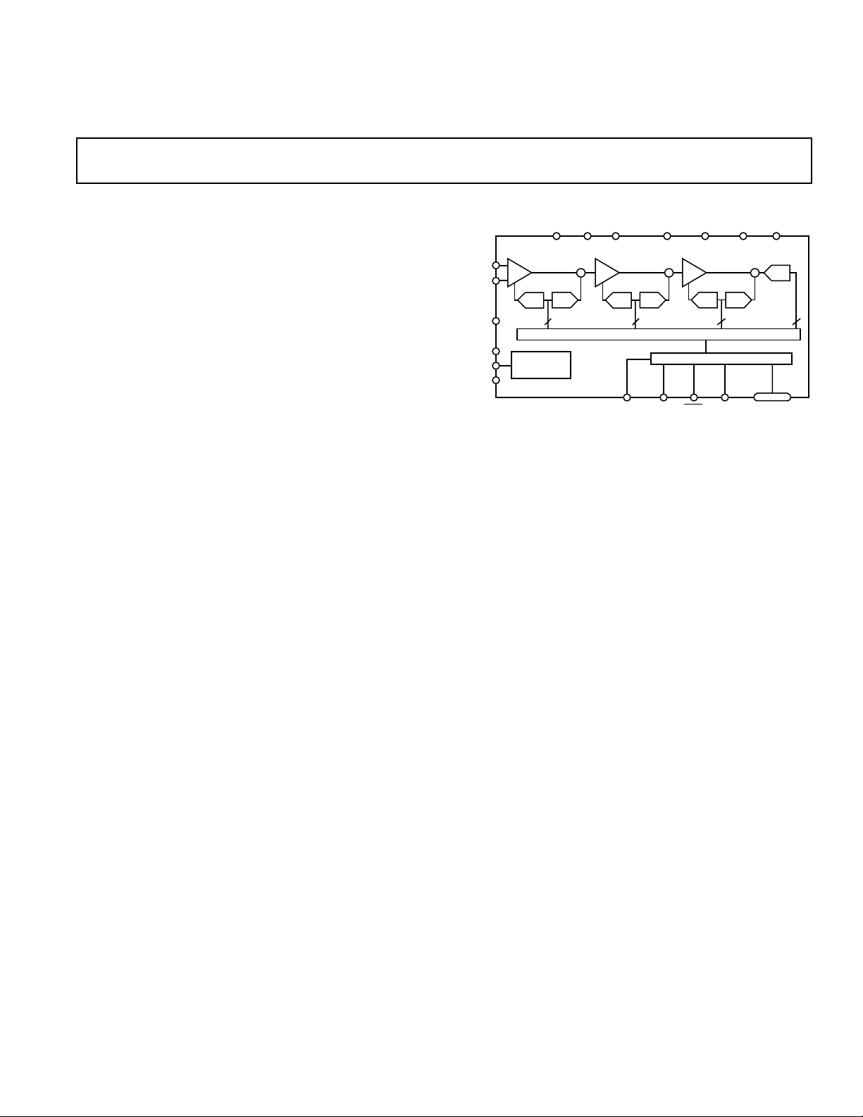
FUNCTIONAL BLOCK DIAGRAM
The AD872A is fabricated on Analog Devices’ ABCMOS-l
process that utilizes high speed bipolar and CMOS transistors
on a single chip.
The AD872A is packaged in a 28-lead ceramic DIP and a 44terminal leadless ceramic surface mount package (LCC). Operation is specified from 0°C to +70°C and –55°C to +125°C.
PRODUCT HIGHLIGHTS
The AD872A offers a complete single-chip sampling, 12-bit
10 MSPS analog-to-digital conversion function in a 28-lead DIP
or 44-terminal LCC.
Low Noise—The AD872A features 0.26 LSB rms referred toinput noise.
Low Power—The AD872A at 1.03 W consumes a fraction of the
power of presently available hybrids.
On-Chip Track-and-Hold (T/H)—The low noise, high impedance T/H input eliminates the need for external buffers and can
be configured for single-ended or differential inputs.
Ease of Use—The AD872A is complete with T/H and voltage
reference and is pin-compatible with the AD872.
Out of Range (OTR)—The OTR output bit indicates when the
input signal is beyond the AD872A’s input range.
REV. A
Information furnished by Analog Devices is believed to be accurate and
reliable. However, no responsibility is assumed by Analog Devices for its
use, nor for any infringements of patents or other rights of third parties
which may result from its use. No license is granted by implication or
otherwise under any patent or patent rights of Analog Devices.
One Technology Way , P.O. Box 9106, Norwood, MA 02062-9106, U.S.A.
Tel: 781/329-4700 World Wide Web Site: http://www.analog.com
Fax: 781/326-8703 © Analog Devices, Inc., 1997
Page 2

AD872A–SPECIFICA TIONS
(T
to T
DC SPECIFICATIONS
MIN
Parameter J Grade
, AVDD = + 5 V, DVDD = +5 V, AVSS = –5 V, f
MAX
1
RESOLUTION 12 12 Bits min
MAX CONVERSION RATE 10 10 MHz min
INPUT REFERRED NOISE 0.26 0.26 LSB rms typ
ACCURACY
Integral Nonlinearity (INL) ± 1.75 ±1.75 LSB typ
Differential Nonlinearity (DNL) ±0.5 ±0.5 LSB typ
No Missing Codes 12 12 Bits Guaranteed
Zero Error (@ +25°C)
Gain Error (@ +25°C)
2
2
±0.75 ±0.75 % FSR max
±1.25 ±1.25 % FSR max
TEMPERATURE DRIFT
Zero Error ±0.15 ±0.3 % FSR max
Gain Error
Gain Error
POWER SUPPLY REJECTION
3, 4
3, 5
±0.80 ±1.75 % FSR max
±0.25 ±0.50 % FSR max
6
AVDD, DVDD (+5 V ± 0.25 V) ±0.125 ±0.125 % FSR max
AVSS (–5 V ± 0.25 V) ±0.125 ±0.125 % FSR max
ANALOG INPUT
Input Range ±1.0 ±1.0 V max
Input Resistance 50 50 kΩ typ
Input Capacitance 10 10 pF typ
= 10 MHz unless otherwise noted)
SAMPLE
S Grade
1
Units
INTERNAL VOLTAGE REFERENCE
Output Voltage 2.5 2.5 V typ
Output Voltage Tolerance ±20 ±40 mV max
Output Current (Available for External Loads) 2.0 2.0 mA typ
(External Load Should Not Change During Conversion)
REFERENCE INPUT RESISTANCE 5 5 kΩ
POWER SUPPLIES
Supply Voltages
AV
DD
AV
SS
DV
DRV
DD
DD
7
+5 +5 V (±5% AVDD Operating)
–5 –5 V (±5% AVSS Operating)
+5 +5 V (±5% DVDD Operating)
+5 +5 V (±5% DRVDD Operating)
Supply Current
IAV
DD
IAV
SS
IDV
DD
IDRV
DD
7
91 92 mA max (85 mA typ)
147 150 mA max (115 mA typ)
20 21 mA max (7 mA typ)
22mA
POWER CONSUMPTION 1.03 1.03 W typ
1.25 1.3 W max
NOTES
1
Temperature ranges are as follows: J Grade: 0°C to +70° C, S Grade: –55° C to +125 ° C.
2
Adjustable to zero with external potentiometers (see Zero and Gain Error Calibration section).
3
+25°C to T
4
Includes internal voltage reference drift.
5
Excludes internal voltage reference drift.
6
Change in Gain Error as a function of the dc supply voltage (V
7
LCC package only.
Specifications subject to change without notice.
and +25°C to T
MIN
MAX
.
to V
NOMINAL
MIN
, V
NOMINAL
to V
MAX
).
–2–
REV. A
Page 3
AD872A
AC SPECIFICATIONS
MIN
, AVDD = + 5 V, DVDD = +5 V, AVSS = –5 V, f
MAX
= 10 MHz unless otherwise noted)
SAMPLE
(T
to T
Parameter J Grade S Grade Units
SIGNAL-TO-NOISE & DISTORTION RATIO (S/N+D)
= l MHz 68 68 dB typ
f
INPUT
61 61 dB min
f
= 4.99 MHz 66 66 dB typ
INPUT
SIGNAL-TO-NOISE RATIO (SNR)
f
= 1 MHz 69 69 dB typ
INPUT
f
= 4.99 MHz 67 67 dB typ
INPUT
TOTAL HARMONIC DISTORTION (THD)
= 1 MHz –74 –74 dB typ
f
INPUT
–63 –62 dB max
f
= 4.99 MHz –72 –72 dB typ
INPUT
SPURIOUS-FREE DYNAMIC RANGE (SFDR)
= l MHz 75 75 dB typ
f
INPUT
f
= 4.99 MHz 74 74 dB typ
INPUT
INTERMODULATION DISTORTION (IMD)
2
Second Order Products –80 –80 dB typ
Third Order Products –73 –73 dB typ
FULL POWER BANDWIDTH 35 35 MHz typ
1
SMALL SIGNAL BANDWIDTH 35 35 MHz typ
APERTURE DELAY 6 6 ns typ
APERTURE JITTER 16 16 ps rms typ
ACQUISITION TO FULL-SCALE STEP 40 40 ns typ
OVERVOLTAGE RECOVERY TIME 40 40 ns typ
NOTES
1
f
amplitude = –0.5 dB full scale unless otherwise indicated. All measurements referred to a 0 dB (1.0 V pk) input signal unless otherwise indicated.
INPUT
2
fa = 1.0 MHz, fb = 0.95 MHz with t
Specifications subject to change without notice.
DIGITAL SPECIFICATIONS
SAMPLE
= 10 MHz.
(T
MIN
to T
, AVDD = + 5 V, DVDD = +5 V, AVSS = –5 V, f
MAX
= 10 MHz unless otherwise noted)
SAMPLE
Parameter Symbol J, S Grades Units
LOGIC INPUTS
High Level Input Voltage V
Low Level Input Voltage V
High Level Input Current (V
Low Level Input Current (V
= DVDD)I
IN
= 0 V) I
IN
Input Capacitance C
IH
IL
IH
IL
IN
+2.0 V min
+0.8 V max
115 µA max
115 µA max
5 pF typ
LOGIC OUTPUT
High Level Output Voltage (I
Low Level Output Voltage (I
Output Capacitance C
= 0.5 mA) V
OH
= 1.6 mA) V
OL
OH
OL
OUT
+2.4 V min
+0.4 V max
5 pF typ
Leakage (Three State, LCC Only) IZ ±10 µA max
Specifications subject to change without notice.
REV. A
–3–
Page 4
AD872A
(T
to T
MIN
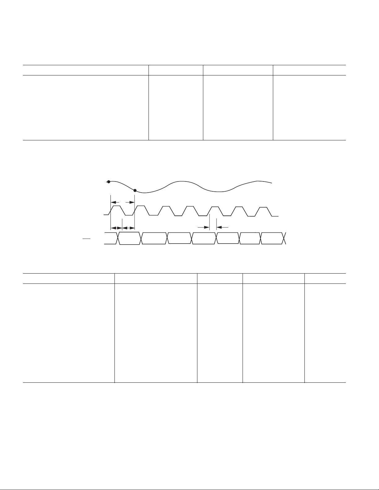
SWITCHING SPECIFICATIONS
VIN = 2.0 V, VOL = 0.4 V and VOH = 2.4 V)
Parameter Symbol J, S Grades Units
Clock Period
1
CLOCK Pulsewidth High t
CLOCK Pulsewidth Low t
Clock Duty Cycle
2
Output Delay t
Pipeline Delay (Latency) 3 Clock Cycles
Data Access Time (LCC Package Only)
Output Float Delay (LCC Package Only)
NOTES
1
Conversion rate is operational down to 10 kHz without degradation in specified performance.
2
See section on Three-State Outputs for timing diagrams and applications information.
Specifications subject to change without notice.
VIN
CLOCK
BIT 2–12
MSB, OTR
N
2
t
N
tCH t
2
N+1
C
N+1
CL
with AVDD = +5 V, DVDD = +5 V, DRVDD = +5 V, AVSS = –5 V; VIL = 0.8 V,
MAX
t
C
CH
CL
100 ns min
45 ns min
45 ns min
40 % min (50% typ)
60 % max
OD
t
DD
t
HL
DATA
N
10 ns min (20 ns typ)
50 ns typ (100 pF Load)
50 ns typ (10 pF Load)
t
OD
DATA
N+1
Figure 1. Timing Diagram
ABSOLUTE MAXIMUM RATINGS
1
Parameter With Respect to Min Max Units
AV
DD
AV
SS
DV
DRV
, DRV
DD
DD
2
DD
2
AGND –0.5 +6.5 Volts
AGND –6.5 +0.5 Volts
DGND, DRGND
DV
DD
2
–0.5 +6.5 Volts
–6.5 +6.5 Volts
DRGND DGND –0.3 +0.3 Volts
AGND DGND –1.0 +1.0 Volts
AV
DD
Clock Input, OEN
2
DV
DD
DGND –0.5 DVDD + 0.5 Volts
Digital Outputs DGND –0.5 DV
, V
V
INA
, REF IN AGND –6.5 +6.5 Volts
INB
REF IN AGND AV
–6.5 +6.5 Volts
+ 0.3 Volts
DD
SS
AV
DD
Volts
Junction Temperature +150 °C
Storage Temperature –65 +150 °C
Lead Temperature (10 sec) +300 °C
NOTES
1
Stresses above those listed under Absolute Maximum Ratings may cause permanent damage to the device. This is a stress rating only; functional operation of the device
at these or any other conditions above those indicated in the operational sections of this specification is not implied. Exposure to absolute maximum ratings for extended
periods may affect device reliability.
2
LCC package only.
REV. A–4–
Page 5
7
17
8
9
10
11
12
13
14
15
16
164044 4142432345
29
39
30
31
32
33
34
35
36
37
38
18 2819 20 21 22 23 24 25 26 27
AD872A
TOP VIEW
(NOT TO SCALE)
OTR
REF GND
MSB
AV
DD
AGND
DGND
AV
SS
AV
DD
V
INAVINB
CLK
REF IN
REF OUT
BIT 12 (LSB)
AV
SS
AGND
DRGND
DV
DD
BIT 11
BIT 10
BIT 9
BIT 8
BIT 7
BIT 6
BIT 5
BIT 4
BIT 3
BIT 2
DRV
DD
DRV
DD
DRGND
OEN
BIT 1 (MSB)
NC
NC
NC
NC
NC
NC
NC
NC
NC
NC
NC
NC = NO CONNECT
PIN DESCRIPTION
AD872A
Symbol Pin No. Pin No. Type Name and Function
DIP LCC
V
V
AV
AV
INA
INB
SS
DD
1 1 AI (+) Analog Input Signal on the differential input amplifier.
2 2 AI (–) Analog Input Signal on the differential input amplifier.
3, 25 5, 40 P –5 V Analog Supply.
4 6, 38 P +5 V Analog Supply.
AGND 5, 24 9, 36 P Analog Ground.
DGND 6, 23 10 P Digital Ground.
DV
DD
7, 22 33 P +5 V Digital Supply.
BIT 12 (LSB) 8 16 DO Least Significant Bit.
BIT 2–BIT 11 18–9 26–17 DO Data Bits 2 through 11.
MSB 19 29 DO Inverted Most Significant Bit. Provides twos complement output
data format.
OTR 20 30 DO Out of Range is Active HIGH on the leading edge of Code 0 or the
trailing edge of Code 4096. See Output Data Format Table III.
CLK 21 31 DI Clock Input. The AD872A will initiate a conversion on the rising
edge of the clock input. See the Timing Diagram for details.
REF OUT 26 41 AO +2.5 V Reference Output. Tie to REF IN for normal operation.
REF GND 27 42 AI Reference Ground.
REF IN 28 43 AI Reference Input. +2.5 V input gives ± 1 V full-scale range.
DRV
DD
N/A 12, 32 P +5 V Digital Supply for the output drivers.
NC N/A 3, 4, 7, 8, 14, 15, No Connect.
28, 35, 37, 39, 44
DRGND N/A 11, 34 P Digital Ground for the output drivers. (See section on Power Supply
Decoupling for details on DRV
and DRGND.)
DD
OEN N/A 13 DI Output Enable. See the Three State Output Timing Diagram for details.
BIT 1 N/A 27 DO Most Significant Bit.
TYPE: AI = Analog Input; AO = Analog Output; DI = Digital Input; DO = Digital Output; P = Power; N/A = Not Available on 28-lead DIP. Only available on
44-terminal surface mount package.
PIN CONFIGURATIONS
28-Lead Ceramic DIP 44-Terminal LCC
1
V
INA
V
2
INB
AV
3
REV. A –5–
AV
AGND
DGND
DV
BIT 12 (LSB)
BIT 11
BIT 10
BIT 9
BIT 8
BIT 7
BIT 6
SS
DD
DD
4
5
AD872A
6
TOP VIEW
(Not to Scale)
7
8
9
10
11
12
13
14
28
27
26
25
24
23
22
21
20
19
18
17
16
15
REF IN
REF GND
REF OUT
AV
SS
AGND
DGND
DV
DD
CLK
OTR
MSB
BIT 2
BIT 3
BIT 4
BIT 5
Page 6

AD872A
DEFINITIONS OF SPECIFICATIONS
LINEARITY ERROR (INL)
Linearity error refers to the deviation of each individual code
from a line drawn from “negative full scale” through “positive
full scale.” The point used as “negative full scale” occurs
1/2 LSB before the first code transition. “Positive full scale” is
defined as a level 1 1/2 LSB beyond the last code transition.
The deviation is measured from the middle of each particular
code to the true straight line.
DIFFERENTIAL LINEARITY ERROR (DNL, NO MISSING
CODES)
An ideal ADC exhibits code transitions that are exactly 1 LSB
apart. DNL is the deviation from this ideal value. Guaranteed
no missing codes to 12-bit resolution indicates that all 4096
codes must be present over all operating ranges.
ZERO ERROR
The major carry transition should occur for an analog value
1/2 LSB below analog common. Zero error is defined as the
deviation of the actual transition from that point. The zero error
and temperature drift specify the initial deviation and maximum
change in the zero error over temperature.
GAIN ERROR
The first code transition should occur for an analog value
1/2 LSB above nominal negative full scale. The last transition
should occur for an analog value 1 1/2 LSB below the nominal
positive full scale. Gain error is the deviation of the actual difference between first and last code transitions and the ideal difference between first and last code transitions.
OVERVOLTAGE RECOVERY TIME
Overvoltage recovery time is defined as that amount of time required for the ADC to achieve a specified accuracy after an
overvoltage (50% greater than full-scale range), measured from
the time the overvoltage signal reenters the converter’s range.
DYNAMIC SPECIFICATIONS
SIGNAL-TO-NOISE AND DISTORTION (S/N+D) RATIO
S/N+D is the ratio of the rms value of the measured input signal
to the rms sum of all other spectral components below the
Nyquist frequency, including harmonics but excluding dc. The
value for S/N+D is expressed in decibels.
TOTAL HARMONIC DISTORTION (THD)
THD is the ratio of the rms sum of the first six harmonic components to the rms value of the measured input signal and is expressed as a percentage or in decibels.
INTERMODULATION DISTORTION (IMD)
With inputs consisting of sine waves at two frequencies, fa and
fb, any device with nonlinearities will create distortion products,
of order (m + n), at sum and difference frequencies of mfa ±
nfb, where m, n = 0, 1, 2, 3 . . . . Intermodulation terms are
those for which m or n is not equal to zero. For example, the
second order terms are (fa + fb) and (fa – fb), and the third order terms are (2 fa + fb), (2 fa – fb), (fa + 2 fb) and (2 fb – fa).
The IMD products are expressed as the decibel ratio of the rms
sum of the measured input signals to the rms sum of the distortion terms. The two signals are of equal amplitude and the peak
value of their sums is –0.5 dB from full scale. The IMD products are normalized to a 0 dB input signal.
TEMPERATURE DRIFT
The temperature drift for zero error and gain error specifies the
maximum change from the initial (+25°C) value to the value at
T
or T
MIN
POWER SUPPLY REJECTION
MAX
.
The specifications show the maximum change in the converter’s
full scale as the supplies are varied from nominal to min/max
values.
APERTURE JITTER
Aperture jitter is the variation in aperture delay for successive
samples and is manifested as noise on the input to the A/D.
APERTURE DELAY
Aperture delay is a measure of the Track-and-Hold Amplifier
(THA) performance and is measured from the rising edge of the
clock input to when the input signal is held for conversion.
FULL-POWER BANDWIDTH
The full-power bandwidth is that input frequency at which the
amplitude of the reconstructed fundamental is reduced by 3 dB
for a full-scale input.
SPURIOUS FREE DYNAMIC RANGE
The difference, in dB, between the rms amplitude of the input
signal and the peak spurious signal.
ORDERING GUIDE
Model Temperature Range Package Option
1
AD872AJD 0°C to +70°C D-28
AD872AJE 0°C to +70°C E-44A
AD872ASD
AD872ASE
NOTES
1
D = Ceramic DIP, E = Leadless Ceramic Chip Carrier.
2
MIL-STD-883 version will be available; contact factory.
2
–55°C to +125°C D-28
2
–55°C to +125°C E-44A
REV. A–6–
Page 7

Dynamic Characteristics–Sample Rate: 10 MSPS–AD872A
–70
–75
–80
–85
–90
–95
2ND
HARMONIC
THD
3RD
HARMONIC
AMPLITUDE – dB
105 106 10
7
INPUT FREQUENCY – Hz
70
68
66
64
62
60
58
S/(N+D) – dB
56
54
52
50
105 106 10
INPUT FREQUENCY – Hz
–0.5 dB
–6.0 dB
7
Figure 2. AD872A S/(N+D) Input Frequency
1
fIN = 1MHz
f
AMPLITUDE = –0.5dB
IN
THD = 73dB
S/(N+D) = 68dB
SNR = 70dB
SFDR = 73dB
15dB/ DIV
9
Figure 4. AD872A Typical FFT, fIN = 1 MHz, fIN Amplitude = –0.5 dB
1
f
= 1MHz
IN
fIN AMPLITUDE = –6.0dB
THD = –77dB
S/(N+D) = 65dB
SNR = 65dB
SFDR = 81dB
Figure 3. AD872A Distortion vs. Input Frequency,
Full-Scale Input
HARMONICS – dB
2ND –73
3RD –82
4TH –87
5TH –90
6TH –92
7TH –95
8TH –95
9TH –93
2
3
8
7
HARMONICS – dB
2ND –81
3RD –97
4TH –91
5TH –84
6TH –88
7TH –90
8TH –90
9TH –94
4
6
5
15dB/ DIV
REV. A – 7 –
Figure 5. AD872A Typical FFT, f
2
9
8
= 1 MHz, fIN Amplitude = –6 dB
IN
7
3
6
4
5
Page 8

AD872A–Dynamic Characteristics–Sample Rate: 10 MSPS
100
90
80
70
60
50
40
30
20
10
0
CODE X
CODE X + 1
0.26 LSB RMS
100 x p(≥ CODE X + 1)
1
15dB/ DIV
9
4
HARMONICS – dB
2ND –75
3RD –88
4TH –93
5TH –87
6TH –86
7TH –90
8TH –91
9TH –94
f
= 750kHz
IN
f
AMPLITUDE = –0.5dB
IN
THD = –74dB
S/(N+D) = 69dB
SNR = 71dB
SFDR = 75dB
2
3
Figure 6. AD872A Typical FFT, fIN = 750 kHz
fIN = 5MHz
fIN AMPLITUDE = –0.5dB
THD = –74dB
S/(N+D) = 65dB
SNR = 65dB
SFDR = 69dB
HARMONICS – dB
2ND –75
3RD –93
4TH –85
5TH –85
6TH –89
7TH –97
8TH –90
9TH –92
5
8
6
7
1
2
4
15dB/ DIV
Figure 7. AD872A Typical FFT, f
700000
600000
500000
400000
300000
NUMBER OF CODE HITS
200000
100000
0
–1 0 +1
DEVIATION FROM CORRECT CODE – LSB
618061
15170 19559
Figure 8. AD872A Output Code Histogram for DC Input
5
9
= 5 MHz
IN
Figure 9. AD872A Code Probability at a Transition
REV. A–8–
Page 9

AD872A
+5V
1.75mA
+1.6V
5pF
–1.9V
–5V
1.75mA
V
INA
OR V
INB
61V
AD872A
–1 –0.8 –0.6 –0.4 –0.2 0 0.2 0.4 0.6 0.8 1.0
CM INPUT VOLTAGE – V
0
–10
–20
–30
–40
–50
–60
–70
–80
–90
–100
THD – dB
THEORY OF OPERATION
The AD872A is implemented using a 4-stage pipelined multiple
flash architecture. A differential input track-and-hold amplifier
(THA) acquires the input and converts the input voltage into a
differential current. A 4-bit approximation of the input is made
by the first flash converter, and an accurate analog representation of this 4-bit guess is generated by a digital-to-analog converter. This approximation is subtracted from the THA output
to produce a remainder, or residue. This residue is then sampled and held by the second THA, and a 4-bit approximation is
generated and subtracted by the second stage. Once the second
THA goes into hold, the first stage goes back into track to
acquire a new input signal. The third stage provides a 3-bit approximation/subtraction operation, and produces the final residue, which is passed to a final 4-bit flash converter. The 15
output bits from the 4 flash converters are accumulated in the
correction logic block, which adds the bits together using the
appropriate correction algorithm, to produce the 12-bit output
word. The digital output, together with overrange indicator, is
latched into an output buffer to drive the output pins.
The additional THA inserted in each stage of the AD872A
architecture allows pipelining of the conversion. In essence, the
converter is converting multiple inputs simultaneously, processing them through the converter chain serially. This means that
while the converter is capable of capturing a new input sample
every clock cycle, it actually takes three clock cycles for the conversion to be fully processed and appear at the output. This
“pipeline delay” is often referred to as latency, and is not a concern in most applications, however there are some cases where it
may be a consideration. For example, some applications call for
the A/D converter to be placed in a high speed feedback loop,
where its input is servoed to provide a desired result at the digital output (e.g., offset calibration or zero restoration in video
applications). In these cases the three clock cycle delay through
the pipeline must be accounted for in the loop stability calculations. Also, because the converter is working on three conversions simultaneously, major disruptions to the part (such as a
large glitch on the supplies or reference) may corrupt three data
samples. Finally, there will be a minimum clock rate below
which the THA droop corrupts the signal in the pipeline. In the
case of the AD872A, this minimum clock rate is 10 kHz.
The high impedance differential inputs of the AD872A allow a
variety of input configurations (see APPLYING THE AD872A),
The AD872A converts the voltage difference between the V
and V
(V
pins. For single-ended applications, one input pin
INB
INA
or V
) may be grounded, but even in this case the differ-
INB
ential input can provide a performance boost: for example, for
an input coming from a coaxial cable, V
shield ground, allowing the AD872A to reject shield noise as
common mode. The high input impedance of the device minimizes external driving requirements and allows the user to externally select the appropriate termination impedance for the
application.
The AD872A clock circuitry uses both edges of the clock in its
internal timing circuitry (see spec page for exact timing requirements). The AD872A samples the analog input on the rising
edge of the clock input. During the clock low time (between the
falling edge and rising edge of the clock) the input THA is in
track mode; during the clock high time it is in hold. System disturbances just prior to the rising edge of the clock may cause the
part to acquire the wrong value, and should be minimized.
REV. A –9–
can be tied to the
INB
INA
While the part uses both clock edges for its timing, jitter is only
a significant issue for the rising edge of the clock (see CLOCK
INPUT section).
APPLYING THE AD872A ANALOG INPUTS
The AD872A features a high impedance differential input that
can readily operate on either single-ended or differential input
signals. Table I summarizes the nominal input voltage span for
both single-ended and differential modes, assuming a 2.5 V
reference input.
Table I. Input Voltage Span
V
INA
V
INB
V
INA–VINB
Single-Ended +1 V GND +1 V (Positive Full Scale)
–1 V GND –1 V (Negative Full Scale)
Differential +0.5 V –0.5 V +1 V (Positive Full Scale)
–0.5 V +0.5 V –1 V (Negative Full Scale)
Figure 10 shows an approximate model for the analog input circuit. As this model indicates, when the input exceeds 1.6 V
(with respect to AGND), the input device may saturate, causing
the input impedance to drop substantially and significantly reducing the performance of the part. Input compliance in the
negative direction is somewhat larger, showing virtually no degradation in performance for inputs as low as –1.9 V.
Figure 10. AD872A Equivalent Analog Input Circuit
Figure 11 illustrates the effect of varying the common-mode
voltage of a –0.5 dB input signal on total harmonic distortion.
Figure 11. AD872A Total Harmonic Distortion vs. CM Input
Voltage, f
= 1 MHz, FS = 10 MSPS
IN
Page 10

AD872A
4500
4000
3500
3000
2500
2000
1500
1000
500
0
0 10 20 30 40 50 60 70 80
nsec
CODE OUT
Figure 12 shows the common-mode rejection performance vs.
frequency for a 1 V p-p common-mode input. This excellent
common-mode rejection over a wide bandwidth affords the user
the opportunity to eliminate many potential sources of input
noise as common mode by using the differential input structure
of the AD872A.
–20
–30
–40
–50
–60
CMR – dB
–70
–80
–90
–100
5
10
6
10
INPUT FREQUENCY – Hz
10
7
8
10
Figure 12. Common-Mode Rejection vs. Input Frequency,
1 V p-p Input
Figures 13 and 14 illustrate typical input connections for singleended inputs.
V
61V
1
INA
AD872A
V
2
INB
Figure 13. AD872A Single-Ended Input Connection
61V
V
1
INA
R
T
AD872A
V
2
INB
562V
562V
V
(60.5V)
U1
IN
536V
536V
U2
V
INA
V
INB
AD872A
Figure 15. Single-Ended to Differential Connections; U1,
U2 = AD811 or AD9617
The use of the differential input signal can help to minimize
even-order distortion from the input THA where performance
beyond –70 dB is desired.
Figure 16 shows the AD872A large signal (–0.5 dB) and small
signal (–20 dB) frequency response.
10
0
–10
–20
FUND AMP – dB
–30
–40
–50
4
10
5
10
10
INPUT FREQUENCY – Hz
6
7
10
8
10
Figure 16. Full Power (–0.5 dB) and Small Signal
Response (–20 dB) vs. Input Frequency
The AD872A’s wide input bandwidth facilitates rapid acquisition of transient input signals: the input THA can typically settle
to 12-bit accuracy from a full-scale input step in less than 40 ns.
Figure 17 illustrates the typical acquisition of a full-scale input
step.
Figure 14. AD872A Single-Ended Input Connection Using
a Shielded Cable
The cable shield is used as a ground connection for the V
put, providing the best possible rejection of the cable noise from
the input signal. Note also that the high input impedance of the
AD872A allows the user to select the termination impedance, be
it 50 ohms, or some other value. Furthermore, unlike many
flash converters, most AD872A applications will not require an
external buffer amplifier. If such an amplifier is required, we
suggest either the AD811 or AD9617.
Figure 15 illustrates how external amplifiers may be used to
convert a single-ended input into a differential signal. The resistor values of 536 Ω and 562 Ω were selected to provide optimum phase matching between U1 and U2.
INB
in-
Figure 17. Typical AD872A Settling Time
REV. A–10–
Page 11

AD872A
1.5 1.7 1.9 2.1 2.3 2.5 2.7 2.9 3.1 3.3 3.5
REFERENCE INPUT VOLTAGE – V
75
70
65
60
55
50
S/(N+D) – dB
The wide input bandwidth and superior dynamic performance
of the input THA make the AD872A suitable for undersampling applications where the input frequency exceeds half the
sample frequency. The input THA is designed to recover rapidly from input overdrive conditions, returning from a 50%
overdrive in less than 40 ns.
Because of the THA’s exceptionally wide input bandwidth,
some users may find the AD872A is sensitive to noise at frequencies from 10 MHz to 50 MHz that other converters are
incapable of responding to. This sensitivity can be mitigated by
careful use of the differential inputs (see previous paragraphs).
Additionally, Figure 18 shows how a small capacitor (10 pF20 pF for 50 Ω terminated inputs) may be placed between V
and V
to help reduce high frequency noise in applications
INB
INA
where limiting the input bandwidth is acceptable.
61V
10 OR 20pF
12V
INA
V
INB
AD872A
Figure 18. Optional High Frequency Noise Reduction
The AD872A will contribute its own wideband thermal noise.
As a result of the integrated wideband noise (0.26 LSB rms,
referred-to-input), applying a dc analog input may produce
more than one code at the output. A histogram of the ADC
output codes, for a dc input voltage, will be between one and
three codes wide, depending on how well the input is centered
on a given code and how many samples are taken. Figure 8
shows a typical AD872A code histogram, and Figure 9 illustrates the AD872A’s transition noise.
REFERENCE INPUT
The nominal reference input should be 2.5 V, taken with respect to REFERENCE GROUND (REF GND). Figure 19 illustrates the equivalent model for the reference input: there is
no clock or signal-dependent activity associated with the reference input circuitry, therefore, no “kickback” into the reference.
AD872A
REF IN
1
5kV
(620%)
The AD872A’s reference input impedance is equal to 5 kΩ
(±20%), and its effective noise bandwidth is 10 MHz, with a
referred-to-input noise gain of 0.8. For example, the internal
reference, with an rms noise of 28 µV (using an external 1 µF
capacitor), contributes 24 µV (0.05 LSB) of noise to the transfer
function of the AD872A.
The full-scale peak-to-peak input voltage is a function of the
reference voltage, according to the equation:
(V
INA=VINB
) Full Scale = 0.8×(V
– REF GND)
REF
Note that the AD872A’s performance was optimized for a 2.5 V
reference input: performance may degrade somewhat for other
reference voltages. Figure 20 illustrates the S/(N+D) performance vs. reference voltage for a 1 MHz, –0.5 dB input signal.
Note also that if the reference is changed during a conversion,
all three conversions in the pipeline will be invalidated.
Figure 20. S/(N+D) vs. Reference Input Voltage,
f
= 1 MHz, FS = 10 MHz
IN
Table II summarizes various 2.5 V references suitable for use
with the AD872A, including the onboard bandgap reference
(see REFERENCE OUTPUT section).
Table II. Suitable 2.5 V References
Drift (ppm/8C) Initial Accuracy %
REF43B 6 (max) 0.2
AD680JN 10 (max) 0.4
Internal 30 (typ) 0.4
REF GND
2
Figure 19. Equivalent Reference Input Circuit
However, in order to realize the lowest noise performance of the
AD872A, care should be taken to minimize noise at the reference input.
REV. A –11–
AV
If an external reference is connected to REF IN, REF OUT
must be connected to +5 V. This should lower the current in
REF GND to less than 350 µA and eliminate the need for a
SS
1 µF capacitor, although decoupling the reference for noise
reduction purposes is recommended.
Alternatively, Figure 21 shows how the AD872A may be driven
from other references by use of an external resistor. The external resistor forms a resistor divider with the on-chip 5 kΩ resistor to realize 2.5 V at the reference input pin (REF IN). A trim
potentiometer is needed to accommodate the tolerance of the
AD872A’s 5 kΩ resistor.
Page 12

AD872A
R
T
+5V REF
2kV 3.9kV
Figure 21. Optional +5 V Reference Input Circuit
REFERENCE GROUND
The REF GND pin provides the reference point for both the
reference input, and the reference output. When the internal
reference is operating, it will draw approximately 500 µA of cur-
rent through the reference ground, so a low impedance path to
the external common is desirable. The AD872A can tolerate a
fairly large difference between REF GND and AGND, up to
+1 V, without any performance degradation.
REFERENCE OUTPUT
The AD872A features an onboard, curvature compensated
bandgap reference that has been laser trimmed for both absolute
value and temperature drift. The output stage of the reference
was designed to allow the use of an external capacitor to limit
the wideband noise. As Figure 22 illustrates, a 1
the reference output is required for stability of the reference output
buffer. Note: If used, an external reference may become unstable
with this capacitor in place.
R
2.5V
REF IN
REF GND
AD872A
5kV
µ
F capacitor on
2.55
2.54
2.53
2.52
2.51
2.50
2.49
2.48
2.47
REFERENCE VOLTAGE – Volts
2.46
2.45
–55
–35
TEMPERATURE – 8C
125
105856545255–15
Figure 23. Reference Output Voltage vs. Temperature
2.50
2.48
2.46
2.44
REFERENCE VOLTAGE – V
2.42
REF IN
0.1mF
1.0mF
+
AD872A
REF GND
REF OUT
Figure 22. Typical Reference Decoupling Connection
With this capacitor in place, the noise on the reference output is
approximately 28 µV rms at room temperature. Figure 23 shows
the typical temperature drift performance of the reference, while
Figure 24 illustrates the variation in reference voltage with load
currents.
The output stage is designed to provide at least 2 mA of output current, allowing a single reference to drive up to four
AD872As, or other external loads. The power supply rejection
of the reference is better than –54 dB at dc.
2.40
1k
10k
REFERENCE OUTPUT LOAD – V
100k
1M
Figure 24. Reference Output Voltage vs. Output Load
DIGITAL OUTPUTS
In 28-lead packages, the AD872A output data is presented in
twos complement format. Table III indicates offset binary and
twos complement output for various analog inputs.
Table III. Output Data Format
Analog Input Digital Output
V
INA–VINB
Offset Binary Twos Complement OTR
≥0.999756 V 1111 1111 1111 0111 1111 1111 1
0.999268 V 1111 1111 1111 0111 1111 1111 0
0 V 100000000000 00000000 0000 0
–1 V 0000 0000 0000 1000 0000 0000 0
–1.000244 V 0000 0000 0000 1000 0000 0000 1
Users requiring offset binary encoding may simply invert the
MSB pin. In the 44-terminal surface mount packages, both
MSB and MSB bits are provided.
The AD872A features a digital out-of-range (OTR) bit that goes
high when the input exceeds positive full scale or falls below
negative full scale. As Table III indicates, the output bits will be
set appropriately according to whether it is an out-of-range high
REV. A–12–
Page 13

AD872A
0 2 4 6 8 10 12 14 16 18 20
S/(N+D) – dB
FREQUENCY – MHz
75
70
65
60
55
50
0 2 4 6 8 10 12 14 16 18 20
FREQUENCY – MHz
1.09
1.08
1.07
1.06
1.05
1.04
POWER – W
condition or an out-of-range low condition. Note that if the input is driven beyond +1.5 V, the digital outputs may not stay at
+FS, but may actually fold back to midscale.
The AD872A’s CMOS digital output drivers are sized to provide sufficient output current to drive a wide variety of logic
families. However, large drive currents tend to cause glitches on
the supplies and may affect S/(N+D) performance. Applications
requiring the AD872A to drive large capacitive loads or large
fanout may require additional decoupling capacitors on DRV
DD
and DVDD. In extreme cases, external buffers or latches could
be used.
THREE-STATE OUTPUTS
The 44-terminal surface mount AD872A offers three-state outputs. The digital outputs can be placed into a three-state mode
by pulling the OUTPUT ENABLE (OEN) pin LOW. Note that
this function is not intended to be used to pull the AD872A on
and off a bus at 10 MHz. Rather, it is intended to allow the ADC
to be pulled off the bus for evaluation or test modes. Also, to
avoid corruption of the sampled analog signal during conversion
(3 clock cycles), it is highly recommended that the AD872A be
placed on the bus prior to the first sampling.
OEN
DATA
OUTPUT
t
DD
THREE-STATE
ACTIVE
t
HL
In this case, a 20 MHz clock is divided by 2 to produce the
10 MHz clock input for the AD872A. In this configuration, the
duty cycle of the 20 MHz clock is irrelevant.
The input circuitry for the CLKIN pin is designed to accommodate both TTL and CMOS inputs. The quality of the logic
input, particularly the rising edge, is critical in realizing the best
possible jitter performance for the part: the faster the rising
edge, the better the jitter performance.
As a result, careful selection of the logic family for the clock
driver, as well as the fanout and capacitive load on the clock
line, is important. Jitter-induced errors become more pronounced at higher frequency, large amplitude inputs, where the
input slew rate is greatest.
The AD872A is designed to support a sampling rate of 10
MSPS; running at slightly faster clock rates may be possible,
although at reduced performance levels. Conversely, some slight
performance improvements might be realized by clocking the
AD872A at slower clock rates. Figure 27 presents the S/(N+D)
vs. clock frequency for a 1 MHz analog input.
Figure 25. Three-State Output Timing Diagram
For timing budgetary purposes, the typical access and float delay times for the AD872A are 50 ns.
CLOCK INPUT
The AD872A internal timing control uses the two edges of the
clock input to generate a variety of internal timing signals. The
optimal clock input should have a 50% duty cycle; however,
sensitivity to duty cycle is significantly reduced for clock rates of
less than 10 megasamples per second.
+5V
R
D
74XX74
20MHz
+5V
Q
Q
S
CLK
Figure 26. Divide-by-Two Clock Circuit
Due to the nature of on-chip compensation circuitry, the duty
cycle should be maintained between 40% and 60% even for
clock rates less than 10 MSPS. One way to realize a 50% duty
cycle clock is to divide down a clock of higher frequency, as
shown in Figure 26.
Figure 27. Typical S/(N+D) vs. Clock Frequency,
f
= 1 MHz, Full-Scale Input
IN
The power dissipated by the correction logic and output buffers
is largely proportional to the clock frequency; running at reduced clock rates provides a slight reduction in power consumption. Figure 28 illustrates this tradeoff.
Figure 28. Typical Power Dissipation vs. Clock Frequency
REV. A –13–
Page 14

AD872A
+2.5V
–2.5V
V
INB
AD872A
0.1mF
10mF
10kV
(a) ZERO TRIM
REF IN
AD872A
TRIM
V
OUT
REF43
(b) GAIN TRIM
100kV
ANALOG SUPPLIES AND GROUNDS
The AD872A features separate analog and digital supply and
ground pins, helping to minimize digital corruption of sensitive
analog signals. In general, AV
and AVDD, the analog supplies,
SS
should be decoupled to AGND, the analog common, as close to
the chip as physically possible. Care has been taken to minimize
the signal dependence of the power supply currents; however,
the analog supply currents will be proportional to the reference
input. With REFIN at 2.5 V, the typical current into AV
85 mA, while the typical current out of AV
is 115 mA. Typi-
SS
DD
is
cally, 30 mA will flow into the AGND pin.
Careful design and the use of differential circuitry provide the
AD872A with excellent rejection of power supply noise over a
wide range of frequencies, as illustrated in Figure 29.
–75
–80
–85
–90
SUPPLY REJECTION – dB
–95
–100
4
10
5
10
FREQUENCY – Hz
AV
SS
AV
DD
DV
DD
6
10
7
10
Figure 29. Power Supply Rejection vs. Frequency,
100 mV p-p Signal on Power Supplies
Figure 30 shows the degradation in SNR resulting from 100 mV
of power supply ripple at various frequencies. As Figure 30
shows, careful decoupling is required to realize the specified dynamic performance. Figure 34 demonstrates the recommended
decoupling strategy for the supply pins. Note that in extremely
noisy environments, a more elaborate supply filtering scheme
may be necessary.
DIGITAL SUPPLIES AND GROUNDS
The digital activity on the AD872A chip falls into two general
categories: CMOS correction logic, and CMOS output drivers.
The internal correction logic draws relatively small surges of
current, mainly during the clock transitions; in the 44-terminal
package, these currents flow through pins DGND and DV
DD
.
The output drivers draw large current impulses while the output
bits are changing. The size and duration of these currents are a
function of the load on the output bits: large capacitive loads are
to be avoided. In the 44-terminal package, the output drivers are
supplied through dedicated pins DRGND and DRV
DD
. Pin
count constraints in the 28-lead packages require that the digital
and driver supplies share package pins (although they have separate bond wires and on-chip routing). The decoupling shown in
Figure 34 is appropriate for a reasonable capacitive load on the
digital outputs (typically 20 pF on each pin). Applications
involving greater digital loads should consider increasing the
digital decoupling proportionately, and/or using external buffers/
latches.
APPLICATIONS
OPTIONAL ZERO AND GAIN TRIM
The AD872A is factory trimmed to minimize zero error, gain
error and linearity errors. In some applications the zero and gain
errors of the AD872A need to be externally adjusted to zero. If
required, both zero error and gain error can be trimmed with external potentiometers as shown in Figure 31. Note that gain error adjustments must be made with an external reference.
Zero trim should be adjusted first. Connect V
to ground and
INA
adjust the 10 kΩ potentiometer such that a nominal digital output code of 0000 0000 0000 (twos complement output) exists.
Note that the zero trim should be decoupled and that the accuracy of the ±2.5 V reference signals will directly affect the offset.
Gain error may then be calibrated by adjusting the REF IN
voltage. The REF IN voltage should be adjusted such that a
+1 V input on V
results in the digital output code 01111
INA
1111 1111 (twos complement output).
70
65
60
SNR – dB
55
50
4
10
Figure 30. SNR vs. Supply Noise Frequency
(f
= 1 MHz)
IN
5
10
FREQUENCY – Hz
10
6
AV
DV
DD
AV
SS
DD
Figure 31. Zero and Gain Error Trims
DIGITAL OFFSET CORRECTION
The AD872A provides differential inputs that may be used to
correct any offset voltages on the analog input. For applications
7
10
where the input signal contains a dc offset, it may be advantageous to apply a nulling voltage to the V
input. Applying a
INB
voltage equal to the dc offset will maximize the full-scale input
range and therefore the dynamic range. Offsets ranging from
–0.7 V to +0.5 V can be corrected.
REV. A–14–
Page 15

AD872A
Figure 32 shows how a dc offset can be applied using the
AD568 12-bit, high speed digital-to-analog converter (DAC).
This circuit can be used for applications requiring offset adjustments on every clock cycle. The AD568 connection scheme is
used to provide a –0.512 V to +0.512 V output range. The offset voltage must be stable on the rising edge of the AD872A
clock input.
DIGITAL
OFFSET
WORD
74
8 8
HC
574
74
HC
574
V
IN
AD568
IBPO
IOUT
RL
44
ACOM
LCOM
REF COM
1
V
AD872A
2
V
INA
INB
Figure 32. Offset Correction Using the AD568
UNDERSAMPLING USING THE AD872A AND AD9100
The AD872A’s on-chip THA optimizes transient response while
maintaining low noise performance. For super-Nyquist (undersampling) applications it may be necessary to use an external
THA with fast track-mode slew rate and hold mode settling
time. An excellent choice for this application is the AD9100, an
ultrahigh speed track-and-hold amplifier.
In order to maximize the spurious free dynamic range of the
circuit in Figure 33 it is advantageous to present a small signal
to the input of the AD9100 and then amplify the output to the
AD872A’s full-scale input range. This can be accomplished with
a low distortion, wide bandwidth amplifier such as the AD9617.
The circuit uses a gain of 3.5 to optimize S/(N+D).
For small scale input signals (–20 dB, –40 dB), the AD872A
performs better without the track-and-hold because slewlimiting effects are no longer dominant. To gain the advantages
of the added track-and-hold, it is important to give the AD872A
a full-scale input.
An alternative to the configuration presented above is to use the
AD9101 track-and-hold amplifier. The AD9101 provides a
built-in post amplifier with a gain of 4, providing excellent ac
characteristics in conjunction with a high level of integration.
As illustrated in Figure 33, it is necessary to skew the AD872A
sample clock and the AD9100 sample/hold control. Clock skew
) is defined as the time starting at the AD9100’s transition
(t
S
into hold mode and ending at the moment the AD872A samples.
The AD872A samples on the rising edge of the sample clock,
and the AD9100 samples on the falling edge of the sample/hold
control. The choice of t
is primarily determined by the settling
S
time of the AD9100. The droop rate of the AD9100 must also
be taken into consideration. Using these values, the ideal t
is
S
17 ns. When choosing clock sources, it is extremely important
that the front end track-and-hold sample/hold control is given a
very low jitter clock source. This is not as crucial for the
AD872A sample clock, because it is sampling a dc signal.
+V
–V
S
S
t
S
1
9
10
= 17ns
5
AD
96685
4
CLOCK 2
CLOCK 1
7Q
8
510
CLOCK 1
IN
R
T
+V
= 5.0V
S
–V
= –5.2V
S
ALL CAPACITORS ARE 0.01mF
(LOW INDUCTANCE - DECOUPLING)
UNLESS OTHERWISE NOTED.
Q
–V
V
S–VS
+V
S
+5V
IN
4
R
T
14
16
20
10mF
AD9100
510
19
18
2
3
8
10
17
13
12
11
10mF
T = 200ns
t
S
6
15
1
5
7
T = 200ns
–V
S
127
2
3
3.3mF
0.1mF
0.1mF
442
7
8*
6
AD
9617
5*
0.1mF
4
0.1mF
3.3mF
–5V
CLOCK 2
IN
AD872A
A
IN
EB
* OPTIONAL, SEE
AD9617 DATASHEET
+5V
0V
+1V
–1V
Figure 33. Undersampling Using the AD872A and AD9100
REV. A –15–
Page 16

AD872A
ANALOG IN
TP1
+5VA
AGND
–5VA
+5VD
DGND
+5A
4
AV
DD
C12
0.1
5
AGND
J1
R1
C6
22mF
JP1
C5
22mF
C21
1mF
10pF
JP2
C4
22mF
49.9
C7
10mF
U2
REF43
1
+5A
2
V
IN
3
V
4
GND
NOTE: JP11 SHOULD BE OPEN
*
C22
0.1
C2
0.01
C1
0.01
C3
0.01
OUT
FB1
FB2
FB3
8
7
6
5
C20
C18
0.1
TP6
C10
0.1
1
V
INA
AD872A
2
V
INB
27
REF GND
28
REF IN
26
REF OUT
JP
11
*
AV
C11
0.1
TP5
+5A
C9
0.1
C8
0.1
–5A
TP3
+5D
AV
SS
–5A
TP4
TP7
DV
DGND
DRV
DGND
MSB
BIT 2
BIT 3
BIT 4
BIT 5
BIT 6
BIT 7
BIT 8
BIT 9
BIT 10
BIT 11
BIT 12
AGND
SS
CLK
OTR
253
+5D
R3
10
7
DD
DD
C17
0.1
C13
0.1
6
22
C15
0.1
23
21
20
19
18
17
16
15
14
13
12
11
10
9
8
24
+5D
CLOCK INPUT
C14
0.1
74HC04
C16
0.1
JP6
49.9
TP2
JP3
R4
P1
40-PIN
IDC CONN.
1
40
R2
JP4
JP8
JP7
3
1
5
2
4
JP9
6
JP10
R5 20
R6 20
R7 20
R8 20
R9 20
R10 20
R11 20
R12 20
R13 20
R14 20
R15 20
R16 20
R17 20
J2
U3
JP5
Figure 34. AD872A/AD871 Evaluation Board Schematic
REV. A–16–
Page 17

AD872A
Figure 35. Silkscreen Layer PCB Layout (Not Shown to Scale)
Table IV. Components List
Reference Designator Description Quantity
R1, R2 Resistor, 1%, Metal Film, 49.9 Ω 2
R3 Resistor, 1%, Metal Film, 10 1
R4–R17 Resistor, 1%, Metal Film, 20 14
C1–C3 SMD Chip Capacitor, 0.01 µF3
C4–C6 Capacitor, Tantalum, 22 µF3
C7 Capacitor, Tantalum, 10 µF1
C8–C19, C22 SMD Chip Capacitor, 0.1 µF13
C20 Capacitor, Mica, 10 pF 1
C21 Capacitor, Ceramic, 1 µF1
U1 AD872A 1
U2 REF43B 1
U3 74HC04N 1
FB1–FB3 Ferrite Bead 3
J1, J2 BNC Jack 2
JP2, 3, 5, 7, 10 Jumpers 5
JP1–JP11 Headers 11
P1 40-Pin IDC Connector 1
REV. A –17–
Page 18

AD872A
Figure 36. Component Side PCB Layout (Not Shown to Scale)
Figure 37. Solder Side PCB Layout (Not Shown to Scale)
REV. A–18–
Page 19

AD872A
Figure 38. Ground Layer PCB Layout (Not Shown to Scale)
Figure 39. Power Layer PCB Layout (Not Shown to Scale)
REV. A –19–
Page 20

AD872A
OUTLINE DIMENSIONS
Dimensions shown in inches and (mm).
28-Lead Side Brazed DIP
(D-28)
0.005 (0.13) MIN
PIN 1
0.225
(5.72)
MAX
0.200 (5.08)
0.125 (3.18)
28
1
0.026 (0.66)
0.014 (0.36)
0.100 (2.54)
0.064 (1.63)
1.490 (37.85) MAX
0.110 (2.79)
0.090 (2.29)
44-Terminal LCC
0.055 (1.40)
0.045 (1.14)
640
0.050
(1.27)
BSC
28
0.100 (2.54) MAX
0.070 (1.78)
0.030 (0.76)
(E-44A)
1
BOTTOM
VIEW
0.662 (16.82)
0.640 (16.27)
15
14
0.075 (1.91) REF
18
SQ
0.610 (15.49)
0.500 (12.70)
0.060 (1.52)
0.015 (0.38)
0.150
(3.81)
MIN
SEATING
PLANE
0.620 (15.75)
0.590 (14.99)
0.018 (0.46)
0.008 (0.20)
0.020 (0.51)
REF x 45°
0.028 (0.71)
0.022 (0.56)
0.040 (1.02)
REF x 45°
3 PLACES
C2001a–0–11/97
PRINTED IN U.S.A.
REV. A–20–
 Loading...