

Page 1
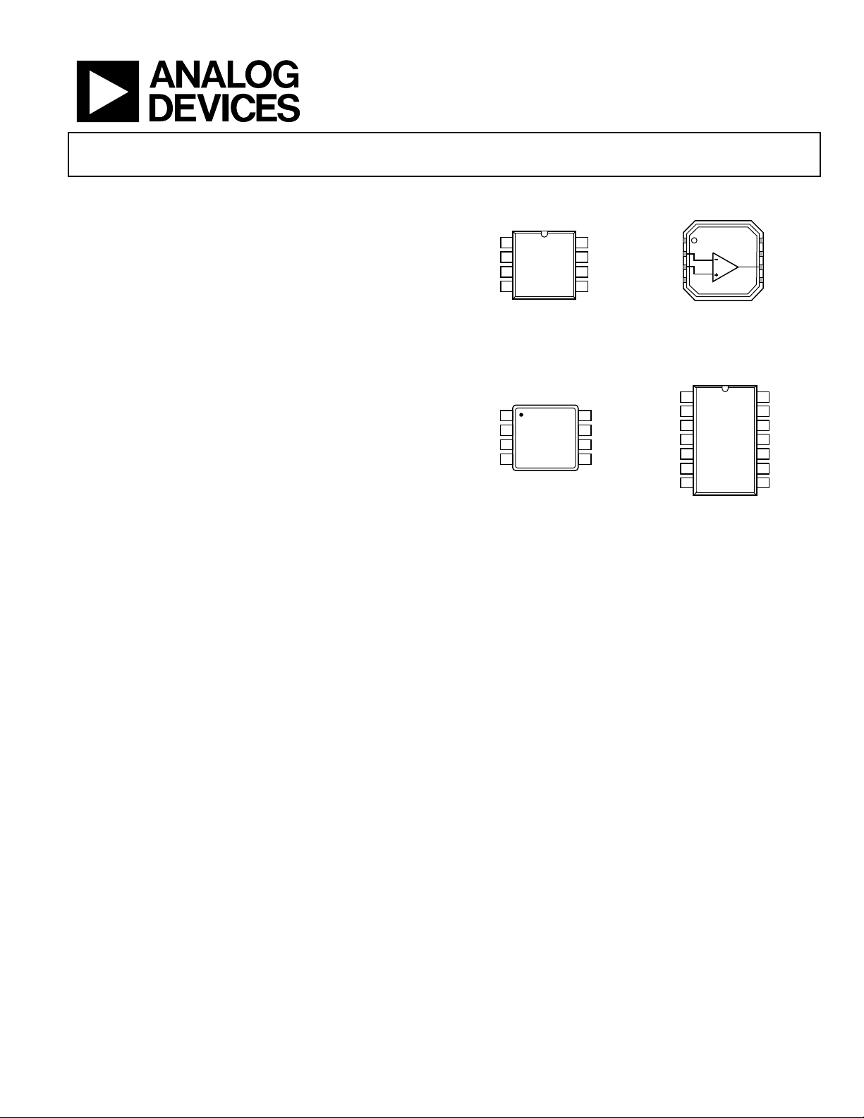
Low Noise, Precision, 16 V, CMOS,
–
FEATURES
Low offset voltage: 175 µV maximum @ VSY = 5 V
Low supply current: 275 A maximum per amplifier
Single-supply operation: 5 V to 16 V
Low noise: 23 nV/√Hz
Low input bias current: 300 fA
Unity-gain stable
Small packages available
3 mm × 3 mm, 8-lead LFCSP
8-lead MSOP
Other packages
8-lead SOIC
14-lead SOIC
14-lead TSSOP
APPLICATIONS
Sensor front ends
Transimpedance amplifiers
Electrometer applications
Photodiode amplification
Low power ADC drivers
Medical diagnostic instruments
pH and ORP meters and probes
DAC or REF buffers
Rail-to-Rail Operational Amplifiers
AD8663/AD8667/AD8669
PIN CONFIGURATIONS
1NC
NC
1
AD8663
IN
2
TOP VIEW
+IN
3
(Not to Scale)
4
V–
NC = NO CONNECT
NC
8
V+
7
OUT
6
5
NC
06742-001
AD8663
2–IN
3+IN
4V–
NC = NO CONNECT
Figure 1. 8-Lead SOIC (R-8) Figure 2. 8-Lead LFCSP (CP-8-2)
OUT A
1
1
2
2
OUT A
–IN A
+IN A
V–
1
AD8667
2
TOP VIEW
3
(Not to Scale)
4
8
7
6
5
Figure 3. 8-Lead MSOP (RM-8),
8-Lead SOIC (R-8)
V+
OUT B
–IN B
+IN B
–IN A
+IN A
3
3
AD8648
AD8669
TOP VIEW
TOP VIEW
V+
4
4
(Not to Scale)
(Not to Scale)
5
5 10
+IN B
06742-003
–IN B
6
6 9
7
7 8
OUT B
Figure 4. 14-Lead SOIC (R-14),
14-Lead TSSOP (RU-14)
8NC
7V+
6OUT
5NC
OUT D
14
14
13
13
–IN D
+IN D
12
12
V–
11
11
10
+IN C
–IN C
9
8
OUT C
06742-002
6742-004
GENERAL DESCRIPTION
The AD866x are rail-to-rail output amplifiers that use the
Analog Devices, Inc., patented DigiTrim® trimming technique
to achieve low offset voltage. The AD866x feature an extended
operating range with supply voltages up to 16 V. They also
feature low input bias current, low input offset voltage, and
low current noise.
The combination of low offset, very low input bias current, and
a wide supply range makes these amplifiers useful in a wide variety
of applications usually associated with higher priced JFET amplifiers. Systems using high impedance sensors, such as photodiodes,
benefit from the combination of low input bias current, low
noise, low offset, and wide bandwidth.
The ability to operate the device for single (5 V to 16 V) or dual
supplies (±2.5 V to ±8 V) supports many applications. The railto-rail outputs provide increased dynamic range to drive low
Rev. B
Information furnished by Analog Devices is believed to be accurate and reliable. However, no
responsibility is assumed by Analog Devices for its use, nor for any infringements of patents or other
rights of third parties that may result from its use. Specifications subject to change without notice. No
license is granted by implication or otherwise under any patent or patent rights of Analog Devices.
Trademarks and registered trademarks are the property of their respective owners.
frequency data converters. The low bias current drift is wellsuited for precision I-to-V converters. The combination of
precision offset, offset drift, and low noise also make the op
amps ideal for gain, dc offset adjust, and active filter in both
instrumentation and medical applications. These low power
op amps can be used in IR thermometers, pH and ORP instruments, pressure transducer front ends, and other sensor signal
conditioning circuits that are used in remote or wireless
applications.
The AD8663/AD8667/AD8669 are specified over the extended
industrial temperature range of −40°C to +125°C. The single
AD8663 is available in a narrow 8-lead SOIC package and a ver y
thin, 8-lead LFCSP. The dual AD8667 is available in a narrow
8-lead SOIC package and an 8-lead MSOP. The quad AD8669
is available in a 14-lead SOIC and 14-lead small TSSOP.
One Technology Way, P.O. Box 9106, Norwood, MA 02062-9106, U.S.A.
Tel: 781.329.4700 www.analog.com
Fax: 781.461.3113 ©2007–2008 Analog Devices, Inc. All rights reserved.
Page 2

AD8663/AD8667/AD8669
TABLE OF CONTENTS
Features .............................................................................................. 1
Applications ....................................................................................... 1
Pin Configurations ........................................................................... 1
General Description ......................................................................... 1
Revision History ............................................................................... 2
Specifications ..................................................................................... 3
Electrical Characteristics ............................................................. 3
REVISION HISTORY
1/08—Rev. A to Rev. B
Added TSSOP ..................................................................... Universal
Change to Table 4 ............................................................................. 5
Changes to Figure 8 and Figure 9 ................................................... 6
Changes to Figure 23 and Figure 26 ............................................... 9
Updated Outline Dimensions ....................................................... 13
Changes to Ordering Guide .......................................................... 15
10/07—Rev. 0 to Rev. A
Added AD8667 and AD8669 ............................................ Universal
Changes to Features .......................................................................... 1
Changes to General Description .................................................... 1
Inserted Figure 3 and Figure 4 ........................................................ 1
Changes to Table 1, Power Supply Section .................................... 3
Changes to Table 2 ............................................................................ 4
Reformatted Typical Performance Characteristics Section ........ 6
Changes to Figure 5 .......................................................................... 6
Changes to Figure 13 ........................................................................ 7
Changes to Figure 17 and Figure 20 ............................................... 8
Inserted Figure 35 Through Figure 39 ......................................... 11
Inserted Figure 40 and Figure 41 .................................................. 12
Updated Outline Dimensions ....................................................... 13
Changes to Ordering Guide .......................................................... 15
7/07—Revision 0: Initial Version
Absolute Maximum Ratings ............................................................5
Thermal Resistance .......................................................................5
ESD Caution...................................................................................5
Typical Performance Characteristics ..............................................6
Outline Dimensions ....................................................................... 13
Ordering Guide .......................................................................... 15
Rev. B | Page 2 of 16
Page 3

AD8663/AD8667/AD8669
SPECIFICATIONS
ELECTRICAL CHARACTERISTICS
VSY = 5.0 V, VCM = VSY/2, TA = 25°C, unless otherwise noted.
Table 1.
Parameter Symbol Conditions Min Typ Max Unit
INPUT CHARACTERISTICS
Offset Voltage VOS V
−40°C < TA < +125°C 450 µV
Input Bias Current IB 0.3 pA
−40°C < TA < +85°C 45 pA
−40°C < TA < +125°C 105 pA
Input Offset Current IOS 0.2 pA
−40°C < TA < +85°C 35 pA
−40°C < TA < +125°C 65 pA
Input Voltage Range 0.2 3.0 V
Common-Mode Rejection Ratio CMRR VCM = 0.2 V to 3.0 V 76 100 dB
−40°C < TA < +125°C 76 100 dB
Large Signal Voltage Gain AVO R
R
Offset Voltage Drift TCVOS −40°C < TA < +125°C 1.5 5 µV/°C
OUTPUT CHARACTERISTICS
Output Voltage High VOH I
−40°C < TA < +125°C 4.90 V
Output Voltage High VOH I
−40°C < TA < +125°C 4.60 V
Output Voltage Low VOL I
−40°C < TA < +125°C 35 mV
Output Voltage Low VOL I
−40°C < TA < +125°C 250 mV
Short-Circuit Current ISC ±7 mA
Closed-Loop Output Impedance Z
f = 100 kHz, AV = 1 120 Ω
OUT
POWER SUPPLY
Power Supply Rejection Ratio PSRR VSY = 5 V to 16 V 95 105 dB
−40°C < TA < +125°C 95 dB
Supply Current per Amplifier ISY V
−40°C < TA < +125°C 325 A
DYNAMIC PERFORMANCE
Slew Rate SR RL = 2 kΩ 0.26 V/µs
Gain Bandwidth Product GBP CL = 20 pF 520 kHz
Phase Margin ΦM C
NOISE PERFORMANCE
Peak-to-Peak Noise en p-p f = 0.1 Hz to 10 Hz 2.5 µV p-p
Voltage Noise Density e
n
f = 10 kHz 21 nV/√Hz
Current Noise Density in f = 1 kHz 0.05 pA/√Hz
= VSY/2 30 175 µV
CM
= 100 kΩ, V
L
= 2 kΩ, V
L
= 100 µA 4.95 4.97 V
L
= 1 mA 4.65 4.80 V
L
= 100 µA 17 25 mV
L
= 1 mA 150 200 mV
L
= VSY/2 210 275 A
OUT
= 20 pF 60 Degrees
L
= 0.5 V to 4.5 V 115 140 dB
OUT
= 0.5 V to 4.5 V 106 114 dB
OUT
f = 1 kHz 23 nV/√Hz
Rev. B | Page 3 of 16
Page 4

AD8663/AD8667/AD8669
VSY = 16.0 V, VCM = VSY/2, TA = 25°C, unless otherwise noted.
Table 2.
Parameter Symbol Conditions Min Typ Max Unit
INPUT CHARACTERISTICS
Offset Voltage VOS V
−40°C < TA < +125°C 500 µV
Input Bias Current IB 0.3 pA
−40°C < TA < +85°C 45 pA
−40°C < TA < +125°C 120 pA
Input Offset Current IOS 0.2 pA
−40°C < TA < +85°C 35 pA
−40°C < TA < +125°C 65 pA
Input Voltage Range 0.2 14.5 V
Common-Mode Rejection Ratio CMRR VCM = 0.2 V to 14.5 V 87 109 dB
−40°C < TA < +125°C 87 109 dB
Large Signal Voltage Gain AVO R
R
Offset Voltage Drift TCVOS −40°C < TA < +125°C 1.5 5 µV/°C
OUTPUT CHARACTERISTICS
Output Voltage High VOH I
−40°C < TA < +125°C 15.90 V
Output Voltage High VOH I
−40°C < TA < +125°C 15.80 V
Output Voltage Low VOL I
−40°C < TA < +125°C 35 mV
Output Voltage Low VOL I
−40°C < TA < +125°C 125 mV
Short-Circuit Current ISC ±50 mA
Closed-Loop Output Impedance Z
f = 100 kHz, AV = 1 100 Ω
OUT
POWER SUPPLY
Power Supply Rejection Ratio PSRR VSY = 5 V to 16 V 95 105 dB
−40°C < TA < +125°C 95 dB
Supply Current per Amplifier ISY V
−40°C < TA < +125°C 355 A
DYNAMIC PERFORMANCE
Slew Rate SR RL = 2 kΩ 0.3 V/µs
Gain Bandwidth Product GBP CL = 20 pF 540 kHz
Phase Margin ΦM C
NOISE PERFORMANCE
Peak-to-Peak Noise en p-p f = 0.1 Hz to 10 Hz 2.5 µV p-p
Voltage Noise Density e
n
f = 10 kHz 21 nV/√Hz
Current Noise Density in f = 1 kHz 0.05 pA/√Hz
= VSY/2 40 300 µV
CM
= 100 kΩ, V
L
= 2 kΩ, V
L
= 100 A 15.95 15.98 V
L
= 1 mA 15.85 15.92 V
L
= 100 A 17 25 mV
L
= 1 mA 70 100 mV
L
= VSY/2 230 285 A
OUT
= 20 pF 64 Degrees
L
= 0.5 V to 15.5 V 115 140 dB
OUT
= 0.5 V to 15.5 V 106 111 dB
OUT
f = 1 kHz 23 nV/√Hz
Rev. B | Page 4 of 16
Page 5
AD8663/AD8667/AD8669
ABSOLUTE MAXIMUM RATINGS
Table 3.
Parameter Rating
Supply Voltage 18 V
Input Voltage −0.1 V to VSY
Differential Input Voltage 18 V
Output Short-Circuit Duration to GND Indefinite
Storage Temperature Range −60°C to +150°C
Operating Temperature Range −40°C to +125°C
Junction Temperature Range −65°C to +150°C
Lead Temperature, Soldering (60 sec) 300°C
Stresses above those listed under Absolute Maximum Ratings
may cause permanent damage to the device. This is a stress
rating only; functional operation of the device at these or any
other conditions above those indicated in the operational
section of this specification is not implied. Exposure to absolute
maximum rating conditions for extended periods may affect
device reliability.
THERMAL RESISTANCE
θJA is specified for the worst-case conditions, that is, a device
soldered in a circuit board for surface-mount packages.
Table 4. Thermal Resistance
Package Type θJA θ
8-Lead SOIC (R-8) 121 43 °C/W
8-Lead LFCSP (CP-8-2) 751 181 °C/W
8-Lead MSOP (RM-8) 145 45 °C/W
14-Lead SOIC (R-14) 90 45 °C/W
14-Lead TSSOP (RU-14) 180 35 °C/W
1
Exposed pad soldered to application board.
Unit
JC
ESD CAUTION
Rev. B | Page 5 of 16
Page 6

AD8663/AD8667/AD8669
TYPICAL PERFORMANCE CHARACTERISTICS
1600
VSY = 5V
1400
1200
1000
NUMBER OF AMPLIFIERS
800
600
400
200
0
–0.1V < V
T
A
<+3.5V
CM
= 25°C
0 50 100 150 200 250–50–100–150–200–250
VOS(µV)
Figure 5. Input Offset Voltage Distribution
06742-005
10000
9000
8000
7000
6000
5000
4000
3000
NUMBER OF AMPL IFIERS
2000
1000
VSY = 16V
0
–0.1V < V
T
A
= 25°C
CM
< +14V
0 50 100 150 200 250–50–100–150–200–250
VOS(µV)
Figure 8. Input Offset Voltage Distribution
06742-037
40
35
30
25
20
15
NUMBER OF AMPLIFIERS
10
5
0
0123 45
TCV
OS
(µV)
VSY = ±2.5V
–40°C < T
< +125°C
A
06742-006
Figure 6. Offset Voltage Drift Distribution
500
VSY = 5V
T
= 25°C
400
A
300
200
100
(µV)
0
OS
V
–100
–200
–300
–400
–500
05
0.5 1.0 1.5 2.0 2.5 3.0 3.5 4.0 4.5
V
(V)
CM
.0
06742-007
Figure 7. Input Offset Voltage vs. Common-Mode Voltage
40
35
30
25
20
15
NUMBER OF AMPLIFIERS
10
5
0
Figure 9. Offset Voltage Drift Distribution
300
VSY = 16V
250
T
= 25°C
A
200
150
100
50
(µV)
0
OS
V
–50
–100
–150
–200
–250
–300
2 4 6 8 10 12 14
01
Figure 10. Input Offset Voltage vs. Common-Mode Voltage
TCVOS(µV/°C)
V
(V)
CM
VSY = ±8V
–40°C < T
< +125°C
A
543210
06742-038
6
06742-010
Rev. B | Page 6 of 16
Page 7

AD8663/AD8667/AD8669
100
80
VSY = 5V
T
= 125°C
A
100
80
VSY = 16V
T
= 125°C
A
60
(pA)
B
I
40
20
0
0.5 4.5
1.0 1.5 2.0 2.5 3.0 3.5 4.0
V
(V)
CM
Figure 11. Input Bias Current vs. Common-Mode Voltage at 125°C
100
90
80
70
60
CMRR (dB)
50
40
30
VSY = 5V
T
= 25°C
A
60
(pA)
B
I
40
20
0
2.5 4.5 6.5 8.5 10.5 12.5 14.5
0.5
(V)
06742-013
V
CM
06742-016
Figure 14. Input Bias Current vs. Common-Mode Voltage at 125°C
100
90
80
70
60
CMRR (dB)
50
40
30
VSY = 16V
T
= 25°C
A
20
100
1k 10k 100k 1M 10M
FREQUENCY (Hz)
Figure 12. CMRR vs. Frequency, VSY = 5 V
10000
VSY = 5V
T
= 25°C
A
1000
100
10
1
OUTPUT SATURATION VOLTAGE (mV)
0.1
0.001 10
VSY – VOH SOURCING
VOL SINKING
0.01 0.1 1
LOAD CURRENT (mA)
Figure 13. Output Swing Saturation Voltage vs. Load Current
20
100
06742-023
1k 10k 100k 1M 10M
FREQUENCY (Hz)
06742-039
Figure 15. CMRR vs. Frequency, VSY = 16 V
10000
VSY = 16V
= 25°C
T
A
1000
100
10
1
OUTPUT SATURATION VOLTAGE (mV)
0.1
0.001 100
06742-011
VSY – VOH SOURCING
VOL SINKING
0.01 0.1 1 10
LOAD CURRENT (mA)
06742-014
Figure 16. Output Swing Saturation Voltage vs. Load Current
Rev. B | Page 7 of 16
Page 8

AD8663/AD8667/AD8669
350
140
300
250
200
150
100
DROP OUT VOLTAGE (mV)
50
0
–25 –10 5 20 35 50 65 80 95 110 125
–40
VSY – VOH @ 1mA
VOL @ 1mA
VOL @ 100µA
VSY – VOH @ 100µA
TEMPERATURE (° C)
Figure 17. Output Voltage Saturation vs. Temperature
120
100
80
60
40
20
0
–20
–40
GAIN (dB) AND PHASE (Degrees)
–60
VSY = 5V
T
A
–80
100 10M
GAIN
= 25°C
1k 10k 100k 1M
PHASE
CL = 200pF
FREQUENCY (Hz)
Figure 18. Open-Loop Gain and Phase Shift vs. Frequency
CL = 0pF
120
100
80
60
40
DROP OUT VOLTAGE (mV)
20
0
–25 –10 5 20 35 50 65 80 95 110 125
–40
06742-044
VSY – VOH @ 1mA
VOL @ 1mA
VSY – VOH @ 100µA
TEMPERATURE (° C)
VOL @ 100µA
06742-045
Figure 20. Output Voltage Saturation vs. Temperature
120
100
80
60
40
20
0
–20
–40
GAIN (dB) AND PHASE (Degrees)
–60
VSY = 16V
T
A
–80
100 10M
06742-017
GAIN
= 25°C
1k 10k 100k 1M
PHASE
CL = 200pF
FREQUENCY (Hz)
CL = 0pF
06742-020
Figure 21. Open-Loop Gain and Phase Shift vs. Frequency
60
G = 100
40
G = 10
20
(dB)
CL
G = 1
A
0
–20
–40
100 10M
1k 10k 100k 1M
FREQUENCY (Hz)
Figure 19. Closed-Loop Gain vs. Frequency
VSY = 5V
= 25°C
T
A
06742-018
Rev. B | Page 8 of 16
60
G = 100
40
G = 10
20
(dB)
CL
G = 1
A
0
–20
–40
100 10M
1k 10k 100k 1M
FREQUENCY (Hz)
VSY = 16V
T
Figure 22. Closed-Loop Gain vs. Frequency, VSY = 16 V
= 25°C
A
06742-021
Page 9

AD8663/AD8667/AD8669
1000
1000
G = 100
100
(Ω)
10
OUT
Z
1
0.1
100
G = 10
G = 1
1k 10k 100k 1M 10M
FREQUENCY (Hz)
VSY = 5V
T
= 25°C
A
Figure 23. Closed-Loop Output Impedance vs. Frequency, VSY = 5 V
PSRR (dB)
–10
–20
90
80
70
60
50
40
30
20
10
0
100
1k 10k 100k 1M 10M
FREQUENCY (Hz)
VSY = 5V
T
= 25°C
A
PSSR+
PSSR–
Figure 24. PSRR vs. Frequency, VSY = 5 V
G = 100
100
(Ω)
10
OUT
Z
1
0.1
100
06742-040
G = 10
G = 1
1k 10k 100k 1M 10M
FREQUENCY (Hz)
VSY = 16V
T
= 25°C
A
06742-041
Figure 26. Closed-Loop Output Impedance vs. Frequency, VSY = 16 V
90
80
70
60
50
40
30
PSRR (dB)
20
10
0
–10
–20
100
06742-024
1k 10k 100k 1M 10M
FREQUENCY (Hz)
PSSR+
PSSR–
VSY = 16V
T
= 25°C
A
06742-027
Figure 27. PSRR vs. Frequency, VSY = 16 V
80
VSY = 5V
T
= 25°C
A
70
60
50
40
30
OVERSHOOT (%)
20
10
0
10
CAPACITANCE (pF )
OS–
OS+
100 1k
Figure 25. Small-Signal Overshoot vs. Load Capacitance, VSY = 5 V
06742-025
Rev. B | Page 9 of 16
80
VSY = 16V
T
= 25°C
A
70
60
50
40
30
OVERSHOOT (%)
20
10
0
10
100 1k
CAPACITANCE (pF )
OS+
OS–
Figure 28. Small-Signal Overshoot vs. Load Capacitance, VSY = 16 V
06742-028
Page 10

AD8663/AD8667/AD8669
VSY = ±2.5V
A
= 1
V
C
= 200pF
L
R
= 2kΩ
L
VSY = ±8V
= 1
A
V
= 200pF
C
L
= 2kΩ
R
L
VOLTAG E (200mV/DIV)
TIME (10µs/DIV)
Figure 29. Large Signal Transient Response, VSY = ±2.5 V
VSY = ±2.5V
A
= 1
V
C
= 200pF
L
R
= 10kΩ
L
VOLTAGE (50mV/DIV)
TIME (2µs/DIV)
Figure 30. Small Signal Transient Response, VSY = ±2.5 V
VOLTAGE (2V/ DIV)
06742-029
TIME (20µs/DIV)
06742-032
Figure 32. Large Signal Transient Response, VSY = ±8 V
VSY = ±8V
= 1
A
V
= 200pF
C
L
= 10kΩ
R
L
VOLTAGE (50mV/DIV)
06742-030
TIME (2µs/DIV)
06742-033
Figure 33. Small Signal Transient Response, VSY = ±8 V
300
250
200
TA = +125°C
TA = +85°C
TA = +25°C
TA = –40°C
150
(µA)
SY
I
100
50
0
2 4 6 8 10 12 14 16
0
(V)
V
SY
Figure 31. AD8663, Supply Current vs. Supply Voltage
06742-042
Rev. B | Page 10 of 16
1200
1000
800
TA = +125°C
TA = +85°C
TA = +25°C
600
(µA)
SY
I
TA = –40°C
400
200
0
2 4 6 8 10 12 14 16
0
(V)
V
SY
Figure 34. AD8669, Supply Current vs. Supply Voltage
06742-043
Page 11

AD8663/AD8667/AD8669
600
550
500
450
400
350
300
(µA)
SY
I
250
200
150
100
50
0
0 2 4 6 8 10121416
V
+125°C
+85°C
+25°C
–40°C
(V)
SY
Figure 35. AD8667, Supply Current vs. Supply Voltage
0.15
VSY = ±2.5V
A
V
T
A
INPUT VOLTAGE (50mV/DIV)
0.10
0.05
–0.05
–0.10
–0.15
–0.20
–0.25
INPUT VOLTAGE
0
OUTPUT VOLTAGE
TIME (20µs/DIV)
Figure 36. Positive Overload Recovery
= –100
= 25°C
4.5
4.0
3.5
3.0
2.5
2.0
1.5
1.0
0.5
0
–0.5
–1.0
–1.5
–2.0
–2.5
–3.0
–3.5
06742-031
OUTPUT VOLTAGE (1V/DIV)
06742-049
1000
100
(nV/ Hz)
n
e
10
1
1 10000
10 100 1000
FREQUENCY (Hz)
VSY = ±2.5V AND ±8V
= 25°C
T
A
Figure 38. Voltage Noise Density
0.15
0.10
INPUT VOLTAGE
OUTPUT VOLTAGE
TIME (20µs/DIV)
INPUT VOLTAGE (50mV/DIV)
0.05
0
–0.05
–0.10
–0.15
–0.20
–0.25
Figure 39. Positive Overload Recovery
VSY = ±8V
= –100
A
V
= 25°C
T
A
27
22
17
12
7
2
–3
–8
–13
06742-034
OUTPUT VOLTAGE (5V/DIV)
06742-046
–0.05
–0.10
–0.15
–0.20
–0.25
INPUT VOLTAGE (50mV/DIV)
–0.30
–0.35
0.05
7.0
0
INPUT VOLTAGE
OUTPUT VOLTAGE
TIME (20µs/DIV)
VSY = ±2.5V
= –100
A
V
= 25°C
T
A
6.5
6.0
5.5
5.0
4.5
4.0
3.5
3.0
2.5
2.0
1.5
1.0
0.5
0
–0.5
–1.0
OUTPUT VOLTAGE (1V/DIV)
06742-050
Figure 37. Negative Overload Recovery
INPUT VOLTAGE (50mV/DIV)
0.05
–0.05
–0.10
–0.15
–0.20
–0.25
–0.30
–0.35
0
INPUT VOLTAGE
TIME (20µs/DIV)
VSY = ±8V
= –100
A
V
= 25°C
T
A
OUTPUT VOLTAGE
Figure 40. Negative Overload Recovery
35
30
25
20
15
10
5
OUTPUT VOLTAGE (5V/DIV)
0
–5
06742-048
Rev. B | Page 11 of 16
Page 12

AD8663/AD8667/AD8669
0
–20
–40
–60
–80
–100
–120
CHANNEL SEPARATIO N (dB)
–140
–160
100 1k 10k 100k
20kΩ
2kΩ
FREQUENCY (Hz)
VSY = ±2.5V
T
= 25°C
A
Figure 41. Channel Separation vs. Frequency
06742-051
0
–20
–40
–60
–80
–100
–120
CHANNEL SEPARATIO N (dB)
–140
–160
100 1k 10k 100k
20kΩ
2kΩ
FREQUENCY (Hz)
VSY = ±8V
T
= 25°C
A
Figure 42. Channel Separation vs. Frequency
06742-047
Rev. B | Page 12 of 16
Page 13

AD8663/AD8667/AD8669
OUTLINE DIMENSIONS
5.00 (0.1968)
4.80 (0.1890)
4.00 (0.1574)
3.80 (0.1497)
0.25 (0.0098)
0.10 (0.0040)
COPLANARITY
0.10
CONTROLL ING DIMENSI ONS ARE IN MILLIMETERS; INCH DI MENSIONS
(IN PARENTHESES) ARE ROUNDED-OFF MILLIMETER EQUIVALENTS FOR
REFERENCE ONLY AND ARE NOT APPROPRI ATE FOR USE IN DESIGN.
85
1
1.27 (0.0500)
SEATING
PLANE
COMPLIANT TO JEDEC STANDARDS MS-012-A A
BSC
6.20 (0.2441)
5.80 (0.2284)
4
1.75 (0.0688)
1.35 (0.0532)
0.51 (0.0201)
0.31 (0.0122)
8°
0°
0.25 (0.0098)
0.17 (0.0067)
0.50 (0.0196)
0.25 (0.0099)
1.27 (0.0500)
0.40 (0.0157)
45°
012407-A
Figure 43. 8-Lead Small Outline Package [SOIC_N]
Narrow Body
(R-8)
Dimensions shown in millimeters and (inches)
INDICATOR
0.90 MAX
0.85 NOM
SEATING
PLANE
3.25
3.00 SQ
2.75
2.95
PIN 1
12° MAX
TOP
VIEW
0.70 MAX
0.65 TYP
0.30
0.23
0.18
2.75 SQ
2.55
0.05 MAX
0.01 NOM
0.20 REF
Figure 44. 8-Lead Lead Frame Chip Scale Package [LFCSP_VD]
3 mm × 3 mm Body, Very Thin, Dual Lead
Dimensions shown in millimeters
0.60 MAX
0.50
0.40
0.30
(CP-8-2)
0.60 MAX
5
EXPOSED
PA D
(BOTTOM VIEW)
4
0.50
BSC
8
1.60
1.45
1.30
1
1.89
1.74
1.59
PIN 1
INDICATOR
61507-B
Rev. B | Page 13 of 16
Page 14

AD8663/AD8667/AD8669
0.95
0.85
0.75
0.15
0.00
COPLANARITY
3.20
3.00
2.80
8
5
4
SEATING
PLANE
5.15
4.90
4.65
1.10 MAX
0.23
0.08
3.20
3.00
1
2.80
PIN 1
0.65 BSC
0.38
0.22
0.10
COMPLIANT TO JEDEC STANDARDS MO-187-AA
8°
0°
0.80
0.60
0.40
Figure 45. 8-Lead Mini Small Outline Package [MSOP]
(RM-8)
Dimensions shown in millimeters
8.75 (0.3445)
8.55 (0.3366)
4.00 (0.1575)
3.80 (0.1496)
14
1
8
6.20 (0.2441)
5.80 (0.2283)
7
1.27 (0.0500)
BSC
0.25 (0.0098)
0.10 (0.0039)
COPLANARIT Y
0.10
CONTROLL ING DIMENSIONS ARE IN MILLIMETERS; INCH DI MENSIONS
(IN PARENTHESES) ARE ROUNDED-O FF MIL LIMETE R EQUIVALENTS FOR
REFERENCE ON LY AND ARE NOT APPROPRI ATE FOR USE IN DESIGN.
0.51 (0.0201)
0.31 (0.0122)
COMPLIANT TO JEDEC STANDARDS MS-012-AB
1.75 (0.0689)
1.35 (0.0531)
SEATING
PLANE
0.25 (0.0098)
0.17 (0.0067)
Figure 46. 14-Lead Small Outline Package [SOIC_N]
Narrow Body
(R-14)
Dimensions shown in millimeters and (inches)
5.10
5.00
4.90
1.05
1.00
0.80
4.50
4.40
4.30
PIN 1
14
0.65
BSC
0.15
0.05
COMPLIANT TO JEDEC STANDARDS MO-153-AB-1
0.30
0.19
8
6.40
BSC
71
1.20
MAX
SEATING
PLANE
0.20
0.09
COPLANARITY
0.10
Figure 47. 14-Lead Thin Shrink Small Outline Package [TSSOP]
(RU-14)
Dimensions shown in millimeters
0.50 (0.0197)
0.25 (0.0098)
8°
0°
1.27 (0.0500)
0.40 (0.0157)
8°
0°
0.75
0.60
0.45
45°
060606-A
Rev. B | Page 14 of 16
Page 15

AD8663/AD8667/AD8669
ORDERING GUIDE
Model Temperature Range Package Description Package Option Branding
AD8663ARZ
AD8663ARZ-REEL
AD8663ARZ-REEL7
AD8663ACPZ-R2
AD8663ACPZ-REEL
AD8663ACPZ-REEL7
AD8667ARZ
AD8667ARZ-REEL
AD8667ARZ-REEL7
AD8667ARMZ-R2
AD8667ARMZ-REEL
AD8669ARZ
AD8669ARZ-REEL
AD8669ARZ-REEL7
AD8669ARUZ
AD8669ARUZ-REEL
1
Z = RoHS Compliant Part.
1
−40°C to +125°C 8-Lead SOIC_N R-8
1
−40°C to +125°C 8-Lead SOIC_N R-8
1
−40°C to +125°C 8-Lead SOIC_N R-8
1
−40°C to +125°C 8-Lead LFCSP_VD CP-8-2 A1U
1
−40°C to +125°C 8-Lead LFCSP_VD CP-8-2 A1U
1
1
1
−40°C to +125°C 8-Lead LFCSP_VD CP-8-2 A1U
−40°C to +125°C 8-Lead SOIC_N R-8
1
1
−40°C to +125°C 14-Lead SOIC_N R-14
1
1
−40°C to +125°C 8-Lead SOIC_N R-8
1
−40°C to +125°C 8-Lead SOIC_N R-8
−40°C to +125°C 8-Lead MSOP RM-8 A1E
1
−40°C to +125°C 8-Lead MSOP RM-8 A1E
−40°C to +125°C 14-Lead SOIC_N R-14
1
−40°C to +125°C 14-Lead SOIC_N R-14
−40°C to +125°C 14-Lead TSSOP RU-14
1
−40°C to +125°C 14-Lead TSSOP RU-14
Rev. B | Page 15 of 16
Page 16

AD8663/AD8667/AD8669
NOTES
©2007–2008 Analog Devices, Inc. All rights reserved. Trademarks and
registered trademarks are the property of their respective owners.
D06742-0-1/08(B)
Rev. B | Page 16 of 16
 Loading...