

Page 1
24 MHz Rail-to-Rail Amplifiers
www.BDTIC.com/ADI
FEATURES
Offset voltage: 2.5 mV maximum
Single-supply operation: 2.7 V to 5.5 V
Low noise: 8 nV/√Hz
Wide bandwidth: 24 MHz
Slew rate: 11 V/μs
Short-circuit output current: 120 mA
No phase reversal
Low input bias current: 1 pA
Low supply current per amplifier: 2 mA maximum
Unity gain stable
APPLICATIONS
Battery-powered instruments
Multipole filters
ADC front ends
Sensors
Barcode scanners
ASIC input or output amplifiers
Audio amplifiers
Photodiode amplifiers
Datapath/mux/switch control
with Shutdown Option
AD8646/AD8647/AD8648
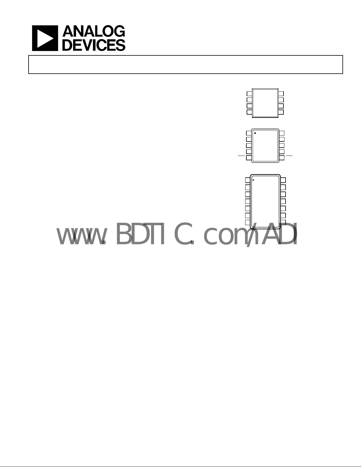
PIN CONFIGURATIONS
1
OUTA
–INA
2
AD8646
V–
TOP VIEW
3
(Not to Scale)
4
+INA
Figure 1. 8-Lead SOIC and MSOP
1
OUTA
–INA
2
V–
AD8647
3
TOP VIEW
(Not to Scale)
4
5
+INA
SDA
Figure 2. 10-Lead MS
1
1
OUTA
2
2
–INA
3
3
+INA
+INB
–INB
OUTB
V+
AD8648
AD8648
TOP VIEW
TOP VIEW
4
4
(Not to Scale)
(Not to Scale)
5
5
6
6
7
7
Figure 3. 14-Lead SOIC and TSSOP
8
7
6
5
10
9
8
7
6
14
14
13
13
12
12
11
11
10
10
V+
OUTB
–INB
+INB
OP
9
9
8
8
V+
OUTB
–INB
+INB
SDB
OUTD
–IND
+IND
V–
+INC
–INC
OUTC
06527-001
06527-002
06527-003
GENERAL DESCRIPTION
The AD8646 and the AD8647 are the dual, and the AD8648 is
the quad, rail-to-rail, input and output, single-supply amplifiers
featuring low offset voltage, wide signal bandwidth, low input
voltage, and low current noise. The AD8647 also has a low
power shutdown function.
The combination of 24 MHz bandwidth, low offset, low noise,
nd very low input bias current makes these amplifiers useful in
a
a wide variety of applications. Filters, integrators, photodiode
amplifiers, and high impedance sensors all benefit from the
combination of performance features. AC applications benefit
Rev. B
Information furnished by Analog Devices is believed to be accurate and reliable. However, no
responsibility is assumed by Anal og Devices for its use, nor for any infringements of patents or ot her
rights of third parties that may result from its use. Specifications subject to change without notice. No
license is granted by implication or otherwise under any patent or patent rights of Analog Devices.
Trademarks and registered trademarks are the property of their respective owners.
from the wide bandwidth and low distortion. TheAD8646/
AD8647/AD8648 offer high output drive capability, which is
excellent for audio line drivers and other low impedance
applications.
Applications include portable and low powered instrumenta-
ion, audio amplification for portable devices, portable phone
t
headsets, barcode scanners, and multipole filters. The ability to
swing rail to rail at both the input and output enables designers
to buffer CMOS ADCs, DACs, ASICs, and other wide output
swing devices in single-supply systems.
One Technology Way, P.O. Box 9106, Norwood, MA 02062-9106, U.S.A.
Tel: 781.329.4700 www.analog.com
Fax: 781.461.3113 ©2006–2007 Analog Devices, Inc. All rights reserved.
Page 2

AD8646/AD8647/AD8648
www.BDTIC.com/ADI
TABLE OF CONTENTS
Features.............................................................................................. 1
Applications....................................................................................... 1
Pin Configurations ........................................................................... 1
General Description ......................................................................... 1
Revision History ............................................................................... 2
Specifications..................................................................................... 3
Absolute Maximum Ratings............................................................ 6
Thermal Resistance ...................................................................... 6
REVISION HISTORY
Revision History: AD8646/AD8647/AD8648
10/07—Revision B: Initial Combined Version
Revision History: AD8646
10/07—Rev. 0 to Rev. B
Combined with AD8648....................................................Universal
Added AD8647 ...................................................................Universal
Deleted Figure 4 and Figure 7......................................................... 7
D
eleted Figure 33............................................................................ 11
8/07—Revision 0: Initial Version
Revision History: AD8648
10/0 7 — R e v. A to Re v. B
Combined with AD8646....................................................Universal
Added AD8647 ...................................................................Universal
ESD Caution...................................................................................6
Typical Performance Characteristics..............................................7
Theory of Operation ...................................................................... 15
Power-Down Operation ............................................................ 15
Multiplexing Operation............................................................. 15
Outline Dimensions....................................................................... 16
Ordering Guide .......................................................................... 18
Deleted Figure 7.................................................................................6
D
eleted Figure 11...............................................................................7
Deleted Figure 16 and Figure 17 .....................................................8
Deleted Figure 24...............................................................................9
Deleted Figure 27, Figure 28, Figure 31, and Figure 32 ............ 10
6/07—Rev. 0 to Rev. A
Changes to General Description .....................................................1
Updated Outline Dimensions....................................................... 12
Changes to Ordering Guide.......................................................... 12
1/06—Revision 0: Initial Version
Rev. B | Page 2 of 20
Page 3

AD8646/AD8647/AD8648
www.BDTIC.com/ADI
SPECIFICATIONS
VSY = 5 V, VCM = VSY/2, TA = +25oC, unless otherwise noted.
Table 1.
Parameter Symbol Conditions Min Typ Max Unit
INPUT CHARACTERISTICS
Offset Voltage V
OS
−40°C < TA < +125°C 3.2 mV
Offset Voltage Drift ∆VOS/∆T −40°C < TA < +125°C 1.8 7.5 V/°C
Input Bias Current I
B
−40°C < TA < +85°C 50 pA
−40°C < TA < +125°C 550 pA
Input Offset Current I
OS
−40°C < TA < +85°C 50 pA
−40°C < TA < +125°C 250 pA
Input Voltage Range V
CM
Common-Mode Rejection Ratio CMRR VCM = 0 V to 5 V 67 84 dB
Large Signal Voltage Gain AVO R
Input Capacitance
Differential C
DIFF
Common Mode CCM 6.7 pF
OUTPUT CHARACTERISTICS
Output Voltage High V
OH
−40°C < TA < +125°C 4.90 V
I
−40°C < TA < +125°C 4.70 V
Output Voltage Low V
OL
−40°C < TA < +125°C 40 mV
I
−40°C < TA < +125°C 200 mV
Output Current I
Closed-Loop Output Impedance Z
sc
OUT
POWER SUPPLY
Power Supply Rejection Ratio PSRR VSY = 2.7 V to 5.5 V 63 80 dB
Supply Current per Amplifier ISY 1.5 2.0 mA
−40°C < TA < +125°C 2.5 mA
Supply Current Shutdown Mode (AD8647) ISD Shutdown of both amplifiers (AD8647 only) 10
−40°C < TA < +125°C 1
SHUTDOWN INPUTS (AD8647)
Logic High Voltage (Enabled) V
Logic Low Voltage (Power-Down) V
Logic Input Current (Per Pin) I
Output Pin Leakage Current
DYNAMIC PERFORMANCE
INH
INL
IN
Slew Rate SR RL = 2 kΩ 11 V/s
Gain Bandwidth Product GBP 24 MHz
Phase Margin Øm 74 Degrees
Settling Time ts To 0.1% 0.5
Amplifier Turn-On Time (AD8647) t
Amplifier Turn-Off Time (AD8647) t
on
off
VCM = 0 V to 5V 0.6 2.5 mV
0.3 1 pA
0.1 0.5 pA
0 5 V
= 2 kΩ, VO = 0.5 V to 4.5 V 104 116 dB
L
2.5 pF
I
= 1 mA 4.98 4.99 V
OUT
= 10 mA 4.85 4.92 V
OUT
I
= 1 mA 8.4 20 mV
OUT
= 10 mA 78 145 mV
OUT
Short circuit ±120 mA
At 1 MHz, AV = 1 5 Ω
nA
μA
−40°C < TA < +125°C +2.0 V
−40°C < TA < +125°C +0.8 V
−40°C < TA < +125°C 1
−40°C < TA < +125°C (shutdown active) 1
μA
nA
μs
25°C, AV = 1, RL = 1 kΩ (see Figure 44)
25°C, AV = 1, RL = 1 kΩ (see Figure 45)
1
1
μs
μs
Rev. B | Page 3 of 20
Page 4

AD8646/AD8647/AD8648
www.BDTIC.com/ADI
Parameter Symbol Conditions Min Typ Max Unit
NOISE PERFORMANCE
Peak-to-Peak Noise en p-p 0.1 Hz to 10 Hz 2.3 V
Voltage Noise Density e
f = 10 kHz 6 nV/√Hz
Channel Separation CS f = 10 kHz −115 dB
f = 100 kHz −110 dB
Total Harmonic Distortion Plus Noise THD + N V p-p = 0.1 V, RL = 600 Ω, f = 25 kHz, TA = 25°C
A
A
n
f = 1 kHz 8 nV/√Hz
= +1 0.010 %
V
= −10 0.021 %
V
Rev. B | Page 4 of 20
Page 5

AD8646/AD8647/AD8648
www.BDTIC.com/ADI
VSY = 2.7 V, VCM = VSY/2, TA = +25oC, unless otherwise noted.
Table 2.
Parameter Symbol Conditions Min Typ Max Unit
INPUT CHARACTERISTICS
Offset Voltage V
OS
−40°C < TA < +125°C 3.2 mV
Offset Voltage Drift ∆VOS/∆T −40°C < TA < +125°C 1.8 7.0 V/°C
Input Bias Current I
B
−40°C < TA < +85°C 50 pA
−40°C < TA < +125°C 550 pA
Input Offset Current I
OS
−40°C < TA < +85°C 50 pA
−40°C < TA < +125°C 250 pA
Input Voltage Range V
CM
Common-Mode Rejection Ratio CMRR VCM = 0 V to 2.7 V 62 79 dB
Large Signal Voltage Gain AVO R
Input Capacitance
Differential C
DIFF
Common Mode CCM 7.8 pF
OUTPUT CHARACTERISTICS
Output Voltage High V
OH
−40°C < TA < +125°C 2.60 V
Output Voltage Low V
OL
−40°C < TA < +125°C 30 mV
Output Current I
Closed-Loop Output Impedance Z
OUT
OUT
POWER SUPPLY
Power Supply Rejection Ratio PSRR VSY = 2.7 V to 5.5 V 63 80 dB
Supply Current per Amplifier ISY 1.6 2.0 mA
−40°C < TA < +125°C 2.5 mA
Supply Current Shutdown Mode (AD8647) ISD Shutdown of both amplifiers (AD8647 only) 10 nA
SHUTDOWN INPUTS (AD8647)
Logic High Voltage (Enabled) V
Logic Low Voltage (Power-Down) V
Logic Input Current (Per Pin) V
Output Pin Leakage Current
DYNAMIC PERFORMANCE
INH
INL
IN
Slew Rate SR RL = 2 kΩ 11 V/s
Gain Bandwidth Product GBP 24 MHz
Phase Margin Ø
m
Settling Time ts To 0.1% 0.3
Amplifier Turn-On Time (AD8647) t
Amplifier Turn-Off Time (AD8647) t
on
off
NOISE PERFORMANCE
Peak-to-Peak Noise en p-p 0.1 Hz to 10 Hz 2.3 V
Voltage Noise Density e
n
f = 10 kHz 6 nV/√Hz
Channel Separation CS f = 10 kHz −115 dB
f = 100 kHz −110 dB
VCM = 0 V to 2.7 V 0.6 2.5 mV
0.2 1 pA
0.1 0.5 pA
0 2.7 V
= 2 kΩ, VO = 0.5 V to 2.2 V 95 102 dB
L
2.5 pF
I
= 1 mA 2.65 2.68 V
OUT
I
= 1 mA 11 25 mV
OUT
Short circuit ±63 mA
At 1 MHz, AV = 1 5 Ω
−40°C < TA < +125°C 1 µA
−40°C < TA < +125°C +2.0 V
−40°C < TA < +125°C +0.8 V
−40°C < TA < +125°C 1 µA
−40°C < TA < +125°C (shutdown active) 1 nA
53 Degrees
μs
25°C, AV = 1, RL = 1 kΩ (see Figure 41)
25°C, AV = 1, RL = 1 kΩ (see Figure 42)
1.2
1
μs
μs
f = 1 kHz 8 nV/√Hz
Rev. B | Page 5 of 20
Page 6
AD8646/AD8647/AD8648
www.BDTIC.com/ADI
ABSOLUTE MAXIMUM RATINGS
Table 3.
Parameter Rating
Supply Voltage 6 V
Input Voltage GND to V
Differential Input Voltage ±3 V
Output Short Circuit to GND Indefinite
Storage Temperature Range −65°C to +150°C
Operating Temperature Range −40°C to +125°C
Lead Temperature (Soldering 60 sec) 300°C
Junction Temperature 150°C
Stresses above those listed under Absolute Maximum Ratings
may cause permanent damage to the device. This is a stress
rating only; functional operation of the device at these or any
other conditions above those indicated in the operational
section of this specification is not implied. Exposure to absolute
maximum rating conditions for extended periods may affect
device reliability.
SY
THERMAL RESISTANCE
θJA is specified for the worst-case conditions, that is, a device
soldered in a circuit board for surface-mount packages.
Table 4. Thermal Resistance
Package Type θJA θ
8-Lead SOIC_N 125 43 °C/W
8-Lead MSOP 210 45 °C/W
10-Lead MSOP 200 44 °C/W
14-Lead SOIC_N 120 36 °C/W
14-Lead TSSOP 180 35 °C/W
ESD CAUTION
Unit
JC
Rev. B | Page 6 of 20
Page 7

AD8646/AD8647/AD8648
www.BDTIC.com/ADI
TYPICAL PERFORMANCE CHARACTERISTICS
300
VSY = 2.7V
V
= 1.35V
CM
T
= 25°C
A
250
2244 AMPLIF IERS
200
150
100
NUMBER OF AMPLIFIERS
50
0
–2.0 2.01.51.00.50–0.5–1.0–1.5
VOS (mV)
06527-004
Figure 4. Input Offset Voltage Distribution
35
VSY = 2.7V
30
–40°C < T
< +125°C
A
200
VSY = 5V
V
= 2.5V
180
CM
T
= 25°C
A
2244 AMPLIF IERS
160
140
120
100
80
60
NUMBER OF AMPLIFIERS
40
20
0
–2.0 2.01.51.00.50–0.5–1.0–1.5
VOS (mV)
06527-007
Figure 7. Input Offset Voltage Distribution
35
VSY = 5V
30
–40°C < T
< +125°C
A
25
20
15
10
NUMBER OF AMPLIFIERS
5
0
07654321
Figure 5. V
TCVOS (µV/°C)
Drift (TCVOS) Distribution
OS
2500
2000
1500
1000
500
0
–500
–1000
INPUT OFFSET VOLTAGE (µV)
–1500
–2000
–2500
03.0
0.5 1. 0 1.5 2.0 2.5
INPUT COMMO N-MODE VOL TAGE (V)
Figure 6. Input Offset Voltage vs. Input Common-Mode Voltage
VSY = 2.7V
T
= 25°C
A
25
20
15
10
NUMBER OF AMPLIFIERS
5
0
087654321
06527-005
Figure 8. V
TCVOS (µV/°C)
Drift (TCVOS) Distribution
OS
06527-008
2500
2000
1500
1000
500
0
–500
–1000
INPUTOFFSETVOLTAGE(µV)
–1500
–2000
–2500
012345
06527-006
INPUT COM MON-M ODE VO LTAGE (V)
Figure 9. Input Offset Voltage vs. Input Common-Mode Voltage
VSY=5V
=25°C
T
A
06527-009
Rev. B | Page 7 of 20
Page 8

AD8646/AD8647/AD8648
www.BDTIC.com/ADI
10000
VSY = 2.7V
T
= 25°C
A
1000
VSY – V
10000
VSY = 5V
T
= 25°C
A
OH
1000
100
10
1
OUTPUT SAT URATION VO LTAGE (mV)
0.1
0.001 1001010.10.01
LOAD CURRENT (mA)
V
OL
Figure 10. Output Saturation Voltage vs. Load Current
25
VSY = 2.7V
I
= 1mA
L
20
V
– V
SY
15
10
5
OUTPUT SAT URATION VO LTAGE (mV)
0
–40 –25 –10 5 20 35 50 65 80 95 1 10 125
TEMPERATURE ( °C)
OH
V
OL
Figure 11. Output Saturation Voltage vs. Temperature
300
VSY = 2.7V
T
= 125°C
A
250
100
10
VSY – V
1
OUTPUT SAT URATION VO LTAGE (mV)
0.1
0.001 10001001010.10.01
06527-010
OH
V
OL
LOAD CURRENT (mA)
06527-013
Figure 13. Output Saturation Voltage vs. Load Current
120
VSY = 5V
100
80
60
40
20
OUTPUT SAT URATION VO LTAGE (mV)
0
–40 –25 –10 5 20 35 50 65 80 95 110 125
06527-011
VSY – VOH= 10mA
V
OL
V
– VOH= 1mA
SY
V
= 1mA
OL
TEMPERATURE ( °C)
= 10mA
06527-014
Figure 14. Output Saturation Voltage vs. Temperature
300
VSY = 5V
T
= 125°C
A
250
200
150
100
INPUT BIAS CURRENT (pA)
50
0
0.50 2.001. 751.501.251.000.75
COMMON-MODE VOLTAGE (V)
Figure 12. Input Bias Current vs. Common-Mode Voltage
06527-012
200
150
100
INPUT BIAS CURRENT (pA)
50
0
0.5 1.0 1.5 2.0 2.5 3.0 3.5 4.0 4.5
COMMON-MODE VOLTAGE (V)
Figure 15. Input Bias Current vs. Common-Mode Voltage
Rev. B | Page 8 of 20
06527-015
Page 9

AD8646/AD8647/AD8648
www.BDTIC.com/ADI
= 1kΩ
= 10pF
0
45
90
80
60
PHASE
40
VSY = 5V
R
CL = 10pF
L
= 1k
0
Ω
45
90
80
60
40
VSY = 2.7V
R
L
C
L
20
0
OPEN-LOOP GAIN (dB)
–20
–40
10k 100M10M
100k 1M
FREQUENCY (Hz)
Figure 16. Open-Loop Gain and Phase vs. Frequency
60
40
20
0
–20
CLOSED-LOOP GAIN (dB)
–40
–60
1k 10k 100k 1M 10M 100M
AV = 100
= 10
A
V
= 1
A
V
FREQUENCY (Hz)
Figure 17. Closed-Loop Gain vs. Frequency
250
VSY = 2.7V
T
= 25°C
A
200
150
(Ω)
OUT
Z
100
= 100
A
50
V
ФM = 52°
A
V
= 10
AV = 1
VSY = 2.7V
T
= 25°C
A
135
180
225
270
20
0
OPEN-LOOP GAIN (dB)
OPEN-LOOP PHASE SHIFT (Degrees)
06527-016
–20
–40
10k 100k 1M 10M 100M
FREQUENCY (Hz)
GAIN
Ф
= 74°
M
135
180
225
270
OPEN-LOOP PHASE SHIFT (Degrees)
06527-019
Figure 19. Open-Loop Gain and Phase vs. Frequency
60
40
20
0
–20
CLOSED-LOOP GAIN (dB)
–40
–60
1k 10k 100k 1M 10M 100M
06527-017
AV = 100
= 10
A
V
= 1
A
V
FREQUENCY (Hz)
Figure 20. Closed-Loop Gain vs. Frequency
VSY = 5V
T
= 25°C
A
06527-020
120
VSY = 5V
T
= 25°C
A
100
= 1
A
80
(Ω)
60
OUT
Z
40
20
A
= 100
V
V
= 10
A
V
0
1 10 100 1k 10k 1M100k
FREQUENCY (kHz)
Figure 18. Z
vs. Frequency
OUT
06527-018
0
1 10 100 1k 10k 1M100k
Figure 21. Z
Rev. B | Page 9 of 20
FREQUENCY (kHz)
vs. Frequency
OUT
06527-021
Page 10

AD8646/AD8647/AD8648
www.BDTIC.com/ADI
100
VSY = 2.7V
T
= 25°C
A
80
100
VSY = 5V
= 25°C
T
A
80
60
CMRR (dB)
40
20
0
1k 100M10M1M100k10k
FREQUENCY (Hz)
06527-022
Figure 22. CMRR vs. Frequency
100
PSRR+
80
60
PSRR–
PSRR (dB)
40
20
VSY = 2.7V
= 25°C
T
A
60
CMRR (dB)
40
20
0
1k 100M10M1M100k10k
FREQUENCY (Hz)
06527-025
Figure 25. CMRR vs. Frequency
100
80
60
PSRR (dB)
40
20
PSRR+
PSRR–
VSY = 5V
T
= 25°C
A
0
1k 10M
10k 100k 1M
FREQUENCY (Hz)
06527-023
Figure 23. PSRR vs. Frequency
60
VSY = ±1.35V
= 25°C
T
A
50
40
30
OVERSHOOT (%)
20
10
0
1100010010
C
LOAD
Figure 24. Overshoot v
–OS
+OS
(pF)
s. Load Capacitance
06527-024
0
1k 10M
10k 100k 1M
FREQUENCY (Hz)
Figure 26. PSRR vs. Frequency
70
VSY = 5V
R
= 10kΩ
L
T
= 25°C
60
A
50
40
OS+
30
OVERSHOOT (%)
20
10
0
10 1000
C
100
LOAD
Figure 27. Overshoot v
OS–
(pF)
s. Load Capacitance
06527-026
06527-027
Rev. B | Page 10 of 20
Page 11

AD8646/AD8647/AD8648
www.BDTIC.com/ADI
VSY = 2.7V, VCM = 1.35V, VIN = 100mV p-p ,
T
= 25°C, RL = 10kΩ, CL = 100pF
A
VSY = 5V, VCM = 2.5V, VIN = 100mV p-p ,
T
= 25°C, RL = 10kΩ, CL = 100pF
A
(50mV/DIV)
(200ns/DIV )
06527-028
Figure 28. Small-Signal Transient Response
VSY = 2.7V, VIN = 2V p-p,
T
= 25°C, RL = 10kΩ, CL = 100pF
A
(2V/DIV)
(200ns/DIV )
06527-029
Figure 29. Large-Signal Transient Response
0.08
VSY = ±2.5V
R
= 600Ω
L
0.07
A
= 1
V
T
= 25°C
A
0.06
(50mV/DIV)
(200ns/DIV )
06527-031
Figure 31. Small-Signal Transient Response
VSY = 5V, VIN = 4V p-p,
T
= 25°C, RL = 10kΩ, CL = 100pF
A
(2V/DIV)
(200ns/DIV )
06527-032
Figure 32. Large-Signal Transient Response
0.08
VSY = ±2.5V
R
= 600Ω
L
0.07
A
= –10
V
T
= 25°C
A
0.06
0.05
0.04
THD + N (%)
0.03
0.02
0.01
0
10 100 1k 10k 100k
FREQUENCY (Hz)
Figure 30. THD + Noise vs. Frequency
06527-030
0.05
0.04
THD + N (%)
0.03
0.02
0.01
0
10 100 1k 10k 100k
Figure 33. THD + Noise vs. Frequency
Rev. B | Page 11 of 20
FREQUENCY (Hz)
06527-033
Page 12

AD8646/AD8647/AD8648
www.BDTIC.com/ADI
0.01
THD + N (%)
0.001
0.0001
1000
100
1
0.1
VSY = 5V
A
= 1
V
BW = 30kHz
R
= 100kΩ
L
f = 1kHz
0.010.001 0.1
OUTPUT AMPLITUDE (V rms)
Figure 37. THD + Noise vs. Output Amplitude
VSY = 5V
10
1
06527-034
VSY = 2.7V TO 5V
= 25°C
T
A
VOLTAGE (1µV/DIV)
TIME (1s/DIV)
6527037
Figure 34. 0.1 Hz to 10 Hz Voltage Noise
1000
100
VSY = 2.7V TO 5V
= 25°C
T
A
10
1
INPUT BIAS CURRENT (pA)
VOLTAGE NOISE DENSI TY (nV/ √Hz)
1
10 10k
100 1k
FREQUENCY (Hz)
06527-035
Figure 35. Voltage Noise Density vs. Frequency
2.5
TA = 25°C
2.0
1.5
1.0
0.5
SUPPLY CURRENT PER AMPLIFIER (mA)
0
05
0.5 1.0 1.5 2.0 2.5 3.0 3.5 4.0 4.5
SUPPLY VOLTAGE (V)
Figure 36. Supply Current per Amplifier vs. Supply Voltage
.0
06527-039
0.1
25 125105806545
TEMPERATURE ( °C)
06527-038
Figure 38. Input Bias Current vs. Temperature
5.0
4.5
4.0
3.5
3.0
2.5
2.0
1.5
OUTPUT SWING (V p-p)
1.0
0.5
0
100 1k 10k
FREQUENCY (kHz)
Figure 39. Maximum Output Swing vs. Frequency
VSY = 5V
V
= 4.9V
IN
A
= 1
V
R
= 10kΩ
L
T
= 25°C
A
06527-036
Rev. B | Page 12 of 20
Page 13

AD8646/AD8647/AD8648
www.BDTIC.com/ADI
4.0
3.5
3.0
2.5
2.0
1.5
1.0
0.5
SUPPLY CURRENT PER AMPLIFIER (mA)
0
–40 120
–200 20406080100
TEMPERATURE ( °C)
V
OUT
VSY = 2.7V
VSY = 5V
= VSY/2
06527-040
0
VSY = 5V
R
= 2kΩ
L
A
= –100
V
–20
T
= 25°C
A
–40
–60
–80
CHANNEL SEPARATION (dB)
–100
–120
1k 10k 10 0k
CS (dB) = 20 log (V
V+
3
V+
+
V
2
IN
V–
–
0
V–
FREQUENCY (Hz)
/100 = VIN)
OUT
U1
VIN = 2V p-p
R3
2kΩ
0
20Ω
U2
5
R1
V–
V–
V+
V+
= 0.5V p-p
V
IN
R2
200Ω
6
7
0
0
06527-042
Figure 40. Supply Current per Amplifier vs. Temperature
SHUTDOWN PIN
VSY = 2.7V
R
= 1kΩ
L
A
= 1
V
T
= 25°C
A
VOLTAGE (1V/DIV)
AMPLIFI ER OUTPUT
TIME (200ns/DIV)
06527-045
VSY = 5V
R
A
T
VOLTAGE (1V/DIV)
Figure 41. Turn-On Time
Figure 43. Channel Separation
= 1kΩ
L
= 1
V
= 25°C
A
TIME (200ns/DIV)
Figure 44. Turn-On Time
SHUTDOWN PIN
AMPLIFI ER OUTPUT
06527-043
SHUTDOWN PIN
VSY = 2.7V
R
= 1kΩ
L
A
= 1
V
T
= 25°C
A
VSY = 5V
R
= 1kΩ
L
A
= 1
V
T
= 25°C
A
VOLTAGE (1V/DIV)
AMPLIFI ER OUTPUT
TIME (200n s/DIV)
06527-046
Figure 42. Turn-Off Time
VOLTAGE (1V/DIV)
Figure 45. Turn-Off Time
Rev. B | Page 13 of 20
SHUTDOWN PIN
AMPLIFIER OUTPUT
TIME (200ns/DIV)
06527-044
Page 14

AD8646/AD8647/AD8648
www.BDTIC.com/ADI
100
VSY = 2.7V
100
VSY = 5V
10
1
(nA)
SY
I
0.1
0.01
–40 80
–25 –10 5 20 35 50 65 12595 110
TEMPERATURE (° C)
Figure 46. Supply Current with Op-Amp Shutdown
vs. Temperature
10
1
(nA)
SY
I
0.1
0.01
–40 80
–25 –10 5 20 35 50 65 12595 110
06527-048
Figure 47. Supply Current with Op-Amp Shutdown
TEMPERATURE (° C)
vs. Temperature
06527-047
Rev. B | Page 14 of 20
Page 15

AD8646/AD8647/AD8648
www.BDTIC.com/ADI
THEORY OF OPERATION
POWER-DOWN OPERATION
The shutdown function of the AD8647 is referenced to the
negative supply voltage of the operational amplifier. A logic
level high (> 2.0 V) enables the device, while a logic level low
(< 0.8 V) disables the device and places the output in a high
impedance condition. Several outputs can be wire-OR’ed, thus
eliminating a multiplexer. The logic input is a high impedance
CMOS input. If dual or split supplies are used, the logic signals
must be properly referred to the negative supply voltage.
MULTIPLEXING OPERATION
Because each op amp has a separate logic input enable pin, the
outputs can be connected together if it can be guaranteed that
only one op amp is active at any time. By connecting the op amps
as shown in
asonably short turn-on and turn-off times, low frequency signal
re
paths can be smoothly selected. The turn-off time is slightly faster
than the turn-on time so, even when using sections from two
different packages, the overlap is less than 300 nanoseconds.
Figure 48, a multiplexer can be eliminated. With the
5kHz
13kHz
1
2kHz
Figure 48. AD8647 Output Switching
2V
1V
0V
8
7
2
3
AD8647
6
5V
10
4
2
1/2
9
1/2
AD8647
1
5
06527-049
5V
0V
TIME (200µs/DIV)
Figure 49. Switching Waveforms
06527-050
Rev. B | Page 15 of 20
Page 16

AD8646/AD8647/AD8648
www.BDTIC.com/ADI
OUTLINE DIMENSIONS
5.00 (0.1968)
4.80 (0.1890)
4.00 (0.1574)
3.80 (0.1497)
0.25 (0.0098)
0.10 (0.0040)
COPLANARITY
0.10
CONTROLL ING DIMENSI ONS ARE IN MILLIMETERS; INCH DI MENSIONS
(IN PARENTHESES) ARE ROUNDED-OFF MILLIMETER EQUIVALENTS FOR
REFERENCE ONLY AND ARE NOT APPROPRI ATE FOR USE IN DES IGN.
85
1
1.27 (0.0500)
SEATING
PLANE
COMPLIANT TO JEDEC STANDARDS MS-012-A A
BSC
6.20 (0.2441)
5.80 (0.2284)
4
1.75 (0.0688)
1.35 (0.0532)
0.51 (0.0201)
0.31 (0.0122)
8°
0°
0.25 (0.0098)
0.17 (0.0067)
0.50 (0.0196)
0.25 (0.0099)
1.27 (0.0500)
0.40 (0.0157)
45°
012407-A
Figure 50. 8-Lead Standard Small Outline Package [SOIC_N]
Nar
row Body
(R-8)
Dimensions shown in millimeters and (inches)
3.20
3.00
2.80
3.20
3.00
2.80
8
1
5
5.15
4.90
4.65
4
PIN 1
0.65 BSC
0.95
0.85
0.75
0.15
0.00
COPLANARITY
0.38
0.22
0.10
COMPLIANT TO JEDEC STANDARDS MO-187-AA
1.10 MAX
SEATING
PLANE
0.23
0.08
8°
0°
0.80
0.60
0.40
Figure 51. 8-Lead Mini Small Outline Package [MSOP]
(RM-8)
Dim
ensions shown in millimeters
Rev. B | Page 16 of 20
Page 17

AD8646/AD8647/AD8648
www.BDTIC.com/ADI
3.10
3.00
2.90
6
3.10
3.00
2.90
PIN 1
0.95
0.85
0.75
0.15
0.05
10
1
0.50 BSC
0.33
0.17
COPLANARITY
0.10
COMPLIANT TO JEDEC STANDARDS MO-187-BA
5.15
4.90
4.65
5
1.10 MAX
0.80
0.60
0.40
SEATING
PLANE
0.23
0.08
8°
0°
Figure 52. 10 Lead Mini Small Outline Package [MSOP]
(R
M-10)
Dimensions shown in millimeters
5.10
5.00
4.90
1.05
1.00
0.80
14
4.50
4.40
4.30
PIN 1
0.65
BSC
0.15
0.30
0.05
0.19
COMPLIANT TO JEDEC STANDARDS MO-153-AB-1
Figure 53. 14-Lead Thin Shrink S
8
6.40
BSC
71
0.20
1.20
0.09
MAX
SEATING
PLANE
COPLANARITY
0.10
mall Outline Package [TSSOP]
(RU-14)
Dimensions shown in millimeters
8°
0°
0.75
0.60
0.45
Rev. B | Page 17 of 20
Page 18

AD8646/AD8647/AD8648
www.BDTIC.com/ADI
4.00 (0.1575)
3.80 (0.1496)
0.25 (0.0098)
0.10 (0.0039)
COPLANARIT Y
0.10
CONTROLL ING DIMENSIONS ARE IN MILLI METERS; INCH DIMENSIONS
(IN PARENTHESES) ARE ROUNDED-O FF MIL LIMETE R EQUIVALENTS FOR
REFERENCE ON LY AND ARE NOT APPROPRI ATE FOR USE IN DESIGN.
8.75 (0.3445)
8.55 (0.3366)
BSC
8
7
6.20 (0.2441)
5.80 (0.2283)
1.75 (0.0689)
1.35 (0.0531)
SEATING
PLANE
0.25 (0.0098)
0.17 (0.0067)
14
1
1.27 (0.0500)
0.51 (0.0201)
0.31 (0.0122)
COMPLIANT TO JEDEC STANDARDS MS-012-AB
0.50 (0.0197)
0.25 (0.0098)
8°
0°
1.27 (0.0500)
0.40 (0.0157)
45°
060606-A
Figure 54. 14-Lead Standard Small Outline Package [SOIC_N]
Nar
row Body
(R-14)
Dimensions shown in millimeters and (inches)
ORDERING GUIDE
Model Temperature Range Package Description Package Option Branding
AD8646ARZ
AD8646ARZ-REEL
AD8646ARZ-REEL7
AD8646ARMZ-R2
AD8646ARMZ-REEL
AD8647ARMZ-R2
AD8647ARMZ-REEL
AD8648ARZ
AD8648ARZ-REEL
AD8648ARZ-REEL7
AD8648ARUZ
AD8648ARUZ-REEL
1
Z = RoHS Compliant Part.
1
1
1
1
1
1
1
1
1
1
1
1
−40°C to +125°C 8-Lead SOIC_N R-8
−40°C to +125°C 8-Lead SOIC_N R-8
−40°C to +125°C 8-Lead SOIC_N R-8
−40°C to +125°C 8-Lead MSOP RM-8 A1V
−40°C to +125°C 8-Lead MSOP RM-8 A1V
−40°C to +125°C 10-Lead MSOP RM-10 A1W
−40°C to +125°C 10-Lead MSOP RM-10 A1W
−40°C to +125°C 14-Lead SOIC_N R-14
−40°C to +125°C 14-Lead SOIC_N R-14
−40°C to +125°C 14-Lead SOIC_N R-14
−40°C to +125°C 14-Lead TSSOP RU-14
−40°C to +125°C 14-Lead TSSOP RU-14
Rev. B | Page 18 of 20
Page 19

AD8646/AD8647/AD8648
www.BDTIC.com/ADI
NOTES
Rev. B | Page 19 of 20
Page 20

AD8646/AD8647/AD8648
www.BDTIC.com/ADI
NOTES
©2006–2007 Analog Devices, Inc. All rights reserved. Trademarks and
registered trademarks are the property of their respective owners.
D06527-0-10/07(B)
Rev. B | Page 20 of 20
 Loading...