

Page 1
Precision Low Power
www.BDTIC.com/ADI
FEATURES
SC70 package
Very low I
Single-supply operation: 5 V to 26 V
Dual-supply operation: ±2.5 V to ±13 V
Rail-to-rail output
Low supply current: 630 µA/amp typ
Low offset voltage: 500 µV max
Unity gain stable
No phase reversal
APPLICATIONS
Photodiode amplifiers
ATEs
Line-powered/battery-powered instrumentation
Industrial controls
Automotive sensors
Precision filters
Audio
GENERAL DESCRIPTION
The AD862x is a precision JFET input amplifier. It features
true single-supply operation, low power consumption, and
rail-to-rail output. The outputs remain stable with capacitive
loads of over 500 pF; the supply current is less than 630 µA/amp.
Applications for the AD862x include photodiode transimpedance
amplification, ATE reference level drivers, battery management,
both line powered and portable instrumentation, and remote
sensor signal conditioning, which includes automotive sensors.
: 1 pA max
B
Single-Supply JFET Amplifiers
AD8625/AD8626/AD8627
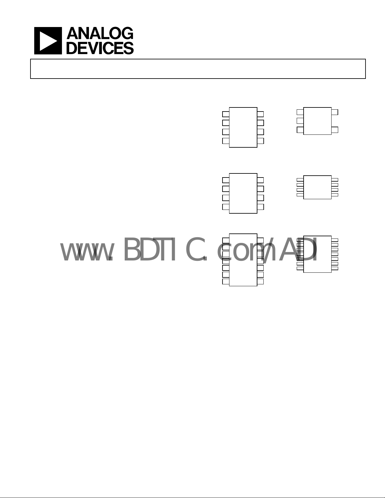
PIN CONFIGURATIONS
8-Lead SOIC
(R-8 Suffix)
NC
1
2
–IN V+
AD8627
3
+IN OUT
4
V– NC
NC = NO CONNECT
8-Lead SOIC
(R-8 Suffix)
OUT A
1
2
–IN A OUT B
+IN A –IN B
OUT A OUT D
–IN A –IN D
+IN A +IN D
+IN B +IN C
–IN B –IN C
OUT B OUT C
AD8626
3
4
V– +IN B
14-Lead SOIC
(R-Suffix)
114
213
312
AD8625
V+ V–
411
510
69
78
NC
8
7
6
5
V+
8
7
6
5
Figure 1.
5-Lead SC70
1
2
V–
+IN
3
8-Lead MSOP
1
4
14-Lead TSSOP
1
7
(KS Suffix)
AD8627
(RM-Suffix)
AD8626
(RU-Suffix)
AD8625
5OUT A
V+
–IN
4
8
V+OUT A
OUT B–IN A
–IN B+IN A
+IN BV–
5
14
OUT DOUT A
–IN D–IN A
+IN D+IN A
V–V+
+IN C+IN B
–IN C–IN B
OUT COUT B
8
03023-001
The AD862x’s ability to swing nearly rail-to-rail at the input
and rail-to-rail at the output enables it to be used to buffer
CMOS DACs, ASICs, and other wide output swing devices in
single-supply systems.
The 5 MHz bandwidth and low offset are ideal for precision
filters.
The AD862x is fully specified over the industrial temperature
range. (–40°C to +85°C). The AD8627 is available in both
5-lead SC70 and 8-lead SOIC surface-mount packages (SC70
packaged parts are available in tape and reel only). The AD8626
is available in MSOP and SOIC packages, while the AD8625 is
available in TSSOP and SOIC packages.
Rev. C
Information furnished by Analog Devices is believed to be accurate and reliable.
However, no responsibility is assumed by Analog Devices for its use, nor for any
infringements of patents or other rights of third parties that may result from its use.
Specifications subject to change without notice. No license is granted by implication
or otherwise under any patent or patent rights of Anal og Devices. Trademarks and
registered trademarks are the property of their respective owners.
One Technology Way, P.O. Box 9106, Norwood, MA 02062-9106, U.S.A.
Tel: 781.329.4700 www.analog.com
Fax: 781.326.8703 © 2004 Analog Devices, Inc. All rights reserved.
Page 2

AD8625/AD8626/AD8627
www.BDTIC.com/ADI
TABLE OF CONTENTS
AD8625/AD8626/AD8627 Specifications..................................... 3
Electrical Characteristics............................................................. 3
Electrical Characteristics............................................................. 4
Absolute Maximum Ratings............................................................ 5
Typical Performance Characteristics............................................. 6
Applications..................................................................................... 13
REVISION HISTORY
11/04—Data Sheet Changed from Rev. B to Rev. C
Updated Figure Codes .......................................................Universal
hanges to Figure 17 and 18........................................................... 8
C
Changes to Figure 33 and Figure 37............................................. 11
Changes to Figure 38...................................................................... 12
Changes to Figure 39 and Figure 40............................................. 13
Changes to Figure 41 to Figure 44................................................ 14
1/04—Data Sheet Changed from Rev. A to Rev. B
Change to General Description...................................................... 1
C
hange to Figure 10 ......................................................................... 7
Change to Figure13 .......................................................................... 7
Change to Figure 37 ....................................................................... 11
Changes to Figure 38...................................................................... 12
Change to Output Amplifier for DACs section.......................... 15
Updated Outline Dimensions....................................................... 19
Minimizing Input Current........................................................ 15
Photodiode Preamplifier Application...................................... 15
Output Amplifier for DACs...................................................... 16
Eight-Pole Sallen Key Low-Pass Filter..................................... 17
Outline Dimensions .......................................................................18
Ordering Guide .......................................................................... 19
10/03—Data Sheet Changed from Rev. 0 to Rev. A
Addition of two new parts
Change to General Description
Changes to Pin Configurations
Change to Specifications table
Changes to Figure 31
Changes to Figure 32
Changes to Figure 38
Changes to Figure 46
Changes to Figure 47
Changes to Figure 49
Updated Outline Dimensions....................................................... 18
Changes to Ordering Guide
…………………………………Universal
………………………………………. 1
…………………....................................1
…………………………………………3
…………………………….................................... 10
…………………………….....................................11
…………………………….................................... 12
…………………………….................................... 16
…………………………….....................................16
…………………………….....................................17
…………………........................................ 19
Rev. C | Page 2 of 20
Page 3

AD8625/AD8626/AD8627
www.BDTIC.com/ADI
AD8625/AD8626/AD8627 SPECIFICATIONS
ELECTRICAL CHARACTERISTICS
@VS = 5 V, VCM = 1.5 V, TA = 25°C, unless otherwise noted.
Table 1.
Parameter Symbol Conditions Min Typ Max Unit
INPUT CHARACTERISTICS
Offset Voltage VOS 0.05 0.5 mV
−40°C < TA < +85°C 1.2 mV
Input Bias Current I
–40°C < TA < +85°C 60 pA
Input Offset Current I
–40°C < TA < +85°C 25 pA
Input Voltage Range 0 3 V
Common-Mode Rejection Ratio CMRR VCM = 0 V to 2.5 V 66 87 dB
Large Signal Voltage Gain A
Offset Voltage Drift ∆VOS/∆T –40°C < TA < +85°C 2.5 µV/°C
OUTPUT CHARACTERISTICS
Output Voltage High V
I
Output Voltage Low V
I
Output Current I
POWER SUPPLY
Power-Supply Rejection Ratio PSRR VS = 5 V to 26 V 80 104 dB
Supply Current/Amplifier I
–40°C < TA < +85°C 800 µA
DYNAMIC PERFORMANCE
Slew Rate SR 5 V/µs
Gain Bandwidth Product GBP 5 MHz
Phase Margin Ø
NOISE PERFORMANCE
Voltage Noise en p-p 0.1 Hz to 10 Hz 1.9 µV p-p
Voltage Noise Density e
Current Noise Density i
Channel Separation C
B
OS
VO
OH
OL
OUT
SY
M
n
n
s
0.25 1 pA
0.5 pA
RL = 10 kΩ, VO = 0.5 V to 4.5 V 100 230 V/mV
4.92 V
= 2 mA, –40°C < TA < +85°C 4.90 V
L
0.075 V
= 2 mA, –40°C < TA < +85°C 0.08 V
L
±10 mA
630 785 µA
60 Degrees
f = 1 kHz 17.5 nV/√Hz
f = 1 kHz 0.4 fA/√Hz
f = 1 kHz 104 dB
Rev. C | Page 3 of 20
Page 4

AD8625/AD8626/AD8627
www.BDTIC.com/ADI
ELECTRICAL CHARACTERISTICS
@VS = ±13 V; VCM = 0 V; TA = 25°C, unless otherwise noted.
Table 2.
Parameter Symbol Conditions Min Typ Max Unit
INPUT CHARACTERISTICS
Offset Voltage V
OS
–40°C < TA < +85°C 1.35 mV
Input Bias Current I
B
–40°C < TA < +85°C 60 pA
Input Offset Current I
OS
–40°C < TA < +85°C 25 pA
Input Voltage Range –13 +11 V
Common-Mode Rejection Ratio CMRR V
Large Signal Voltage Gain A
VO
Offset Voltage Drift ∆VOS/∆T –40°C < TA < +85°C 2.5 µV/°C
OUTPUT CHARACTERISTICS
Output Voltage High V
V
Output Voltage Low V
V
Output Current I
OH
OH
OL
OL
OUT
POWER SUPPLY
Power-Supply Rejection Ratio PSRR VS = ±2.5 V to ±13 V 80 104 dB
Supply Current/Amplifier I
SY
–40°C < TA < +85°C 900 µA
DYNAMIC PERFORMANCE
Slew Rate SR 5 V/µs
Gain Bandwidth Product GBP 5 MHz
Phase Margin Ø
M
NOISE PERFORMANCE
Voltage Noise en p-p 0.1 Hz to 10 Hz 2.5 µV p-p
Voltage Noise Density e
Current Noise Density i
Channel Separation C
n
n
s
0.35 0.75 mV
0.25 1 pA
0.5 pA
= –13 V to +10 V 76 105 dB
CM
RL = 10 kΩ, VO = –11 V to +11 V 150 310 V/mV
+12.92 V
IL = 2 mA, –40°C < TA < +85°C +12.91 V
–12.92 V
IL = 2 mA, –40°C < TA < +85°C –12.91 V
±15 mA
710 850 µA
60 Degrees
f = 1 kHz 16 nV/√Hz
f = 1 kHz 0.5 fA/√Hz
f = 1 kHz 105 dB
Rev. C | Page 4 of 20
Page 5

AD8625/AD8626/AD8627
www.BDTIC.com/ADI
ABSOLUTE MAXIMUM RATINGS
Absolute maximum ratings apply at 25°C, unless otherwise
noted.
Table 3. Stress Ratings
Parameter Ratings
Supply Voltage 27 V
Input Voltage VS– to V
Differential Input Voltage ± Supply Voltage
Output Short-Circuit Duration Indefinite
Storage Temperature Range, R Package
Operating Temperature Range
Junction Temperature Range, R Package
Lead Temperature Range (Soldering, 60 sec) 300°C
Table 4.
Package Type θJA
5-Lead SC70 (KS) 376 126 °C/W
8-Lead MSOP (RM) 210 45 °C/W
8-Lead SOIC (R) 158 43 °C/W
14-Lead SOIC (R) 120 36 °C/W
14-Lead TSSOP (RU) 180 35 °C/W
1
θJA is specified for worst-case conditions when devices are soldered in circuit
boards for surface-mount packages.
1
θ
JC
S+
−65°C to +125°C
−40°C to +85°C
−65°C to +150°C
Unit
Stresses above those listed under Absolute Maximum Ratings
may cause permanent damage to the device. This is a stress
rating only; functional operation of the device at these or any
other conditions above those indicated in the operational
sections of this specification is not implied. Exposure to
absolute maximum rating conditions for extended periods may
affect device reliability.
ESD CAUTION
ESD (electrostatic discharge) sensitive device. Electrostatic charges as high as 4000 V readily accumulate on
the human body and test equipment and can discharge without detection. Although this product features
proprietary ESD protection circuitry, permanent damage may occur on devices subjected to high energy
electrostatic discharges. Therefore, proper ESD precautions are recommended to avoid performance
degradation or loss of functionality.
Rev. C | Page 5 of 20
Page 6
AD8625/AD8626/AD8627
www.BDTIC.com/ADI
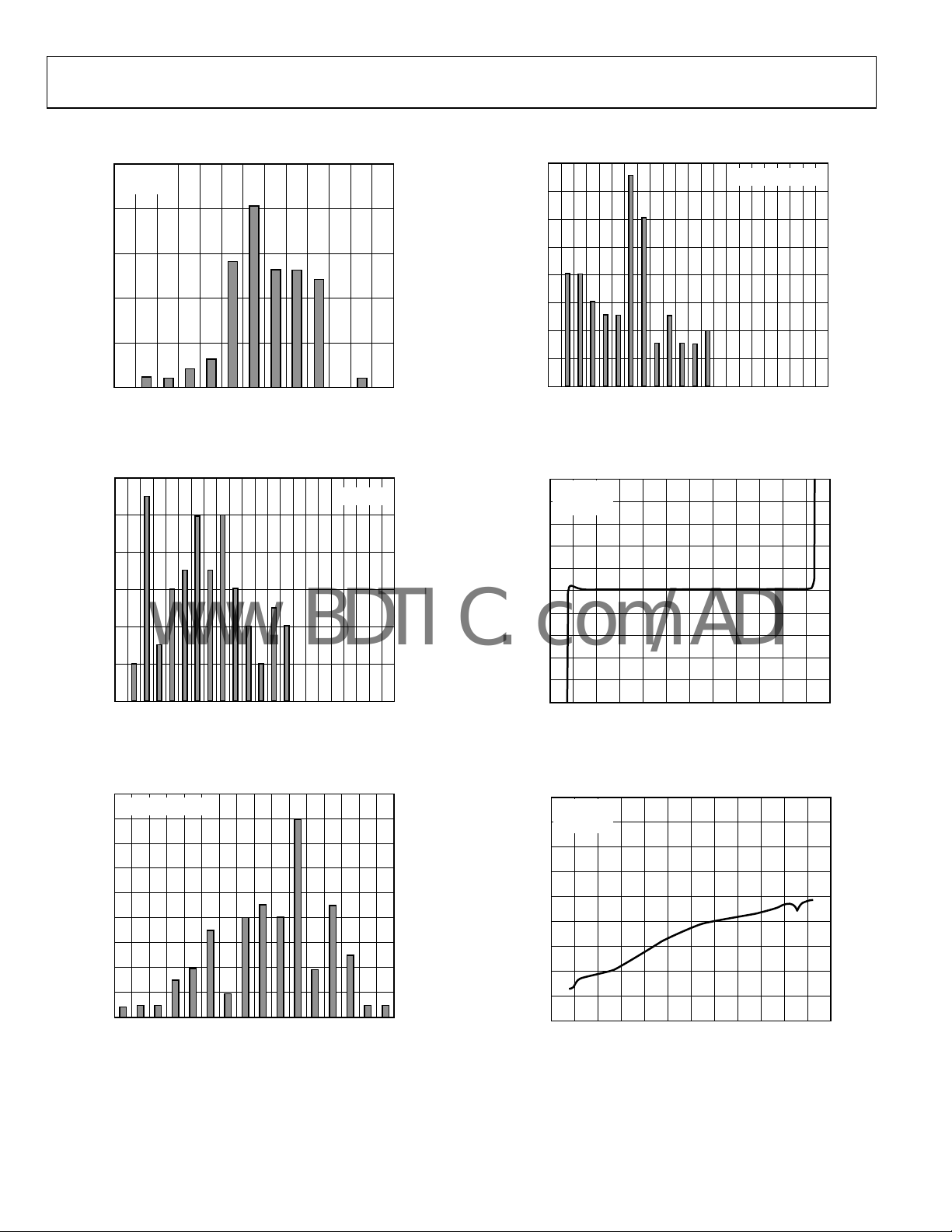
TYPICAL PERFORMANCE CHARACTERISTICS
25
VSY =±12V
= 25°C
T
A
20
16
14
12
VSY = +3.5V/–1.5V
15
10
NUMBER OF AMPLIFIERS
5
0
–600 –400
–200
VOLTAGE (µV)
0 200 400 600
Figure 2. Input Offset Voltage
12
10
8
6
4
NUMBER OF AMPLIFIERS
2
0
012345678910
OFFSET VO LTAGE (µV/°C)
Figure 3. Offset Voltage Drift
18
VSY = +3.5V/–1.5V
16
14
12
10
8
6
NUMBER OF AMPLIFIERS
4
2
0
–400 –300 –200 –100 0 100 200 300
VOLTAGE (µV)
Figure 4. Input Offset Voltage
VSY =±13V
03023-002
03023-003
03023-004
10
8
6
NUMBER OF AMPLIFIERS
4
2
0
012345678910
OFFSET VO LTAGE (µV/°C)
Figure 5. Offset Voltage Drift
50
VSY =±13V
T
= 25°C
40
A
30
20
10
0
–10
–20
INPUT BIAS CURRENT (pA)
–30
–40
–50
–15.0–12.5–10.0 –7.5 –5.0 –2.5 0 2.5 5.0 7.5 10.0 12.5 15.0
Figure 6. Input Bias Current vs. V
VCM (V)
CM
0
VSY =±13V
–0.1
= 25°C
T
A
–0.2
–0.3
–0.4
–0.5
–0.6
INPUT BIAS CURRENT (pA)
–0.7
–0.8
–0.9
–15.0–12.5–10.0 –7.5 –5.0 –2.5 0 2.5 5.0 7.5 10.0 12.5 15.0
Figure 7. Input Bias Current vs. V
VCM (V)
CM
03023-005
03023-006
03023-007
Rev. C | Page 6 of 20
Page 7

AD8625/AD8626/AD8627
www.BDTIC.com/ADI
100
VSY =±13V
V
= 0V
CM
10
1
INPUT BIAS CURRENT (pA)
0.1
–50 –25 0 25 50 75 100 125 150
TEMPERATURE (°C)
Figure 8. Input Bias Current vs. Temperature
2.0
VSY = +5V OR±5V
1.5
1.0
0.5
0
–0.5
–1.0
INPUT BIAS CURRENT (pA)
–1.5
–2.0
–5–4–3–2–1012345
Figure 9. Input Bias Current vs. V
VCM (V)
CM
1000
VSY =±13V
900
800
V)
µ
700
600
500
400
300
200
INPUT OFFSET VOLTAGE (
100
0
–100
–15–12–9–6–303691215
Figure 10. Input Offset Voltage vs. V
VCM (V)
CM
03023-008
03023-009
03023-010
500
VSY = 5V
400
300
V)
µ
200
100
0
–100
–200
INPUT OFFSET VOLTAGE (
–300
–400
–500
–10123
Figure 11. Input Offset Voltage vs. V
VCM (V)
CM
03023-011
4
10M
1M
=±13V
V
SY
VSY = +5V
100k
OPEN-LOOP GAIN (V/V)
10k
0.1 1 10 100
LOAD RESIST ANCE (kΩ)
03023-012
Figure 12. Open-Loop Gain vs. Load Resistance
1000
a
d
b
100
c
e
10
a. VSY =±13V, VO =±11V, RL = 10k
OPEN-LOOP GAIN (V/mV)
b. VSY =±13V, VO =±11V, RL = 2k
c. VSY = +5V, VO = +0.5V/+4.5V, RL = 2k
d. VSY = +5V, VO = +0.5V/+4.5V, RL = 10k
e. VSY = +5V, VO = +0.5V/+4.5V, RL = 600
1
–4025 951
TEMPERATURE (°C)
Ω
Ω
Ω
Ω
Ω
03023-013
25
Figure 13. Open-Loop Gain vs. Temperature
Rev. C | Page 7 of 20
Page 8

AD8625/AD8626/AD8627
www.BDTIC.com/ADI
600
VSY =±13V
500
400
V)
300
µ
OFFSET VOLTAGE (
200
100
–100
–200
–300
–400
= 100k
Ω
R
L
0
–15 –10 –5 0 5 10 15
RL = 600
Ω
OUTPUT VOLTAGE (V)
Figure 14. Input Error Voltage vs. Output Voltage for Resistive Loads
250
V)
µ
INPUT VOLTAGE (
–100
–150
–200
–250
200
150
100
50
–50
POS RAIL
RL = 10k
0
RL = 10k
NEG RAIL
0 50 100 150 200 250 300
OUTPUT VOLTAGE FROM SUPPLY RAILS (mV)
Ω
Ω
R
= 1k
L
RL = 100k
Figure 15. Input Error Voltage vs. Output Voltage within 300 mV of
Supply Rails
800
700
+125°C
A)
600
µ
°
C
500
400
300
200
QUIESCENT CURRENT (
100
0
0 4 8 12 16 20 24 28
+25
TOTAL SUPPLY VOLTAGE (V)
Figure 16. Quiescent Current vs. Supply Voltage at Different Temperatures
RL = 1k
–55
RL = 10k
Ω
=±5V
Ω
V
SY
Ω
Ω
°
C
03023-014
03023-015
03023-016
10k
VSY = ±13V
1k
100
V
– OUTPUT VOLTAGE (mV)
10
SY
V
1
0.001 0.01 0.1 1 10 100
OL
V
OH
LOAD CURRENT (mA)
Figure 17. Output Saturation Voltage vs. Load Current
10k
VSY = 5V
1k
100
V
– OUTPUT VOLTAGE (mV)
10
SY
V
1
0.001 0.01 0.1 1 10 100
OL
V
OH
LOAD CURRENT (mA)
Figure 18. Output Saturation Voltage vs. Load Current
70
60
50
40
30
20
GAIN (dB)
10
0
–10
–20
–30 –135
10k 100k 1M 10M 50M
GAIN
FREQUENCY (Hz)
VSY =±13V
R
= 2k
Ω
L
CL = 40pF
PHASE
Figure 19. Open-Loop Gain and Phase Margin vs. Frequency
315
270
225
180
135
90
45
–0
–45
–90
03023-017
03023-018
PHASE (Degrees)
03023-019
Rev. C | Page 8 of 20
Page 9

AD8625/AD8626/AD8627
www.BDTIC.com/ADI
70
60
50
40
30
20
GAIN (dB)
10
0
–10
–20
–30 –135
10k 100k 1M 10M 50M
GAIN
FREQUENCY (Hz)
VSY = 5V
R
CL = 40pF
PHASE
L
= 2k
Ω
Figure 20. Open-Loop Gain and Phase Margin vs. Frequency
70
VSY =±13V
60
R
= 2k
Ω
L
CL = 40pF
50
40
G = +100
30
20
G = +10
GAIN (dB)
10
0
G = +1
–10
–20
–30
1k 10k 100k 1M 10M 50M
FREQUENCY (Hz)
Figure 21. Closed-Loop Gain vs. Frequency
70
VSY = 5V
60
R
= 2k
Ω
L
CL = 40pF
50
40
G = +100
30
20
G = +10
GAIN (dB)
10
0
G = +1
–10
–20
–30
1k 10k 100k 1M 10M 50M
FREQUENCY (Hz)
Figure 22. Closed-Loop Gain vs. Frequency
315
270
225
180
135
90
45
–0
–45
–90
PHASE (Degrees)
03023-020
03023-021
03023-022
140
VSY =±13V
120
100
80
60
40
CMRR (dB)
20
0
–20
–40
–60
1k 10k 100k 1M 10M
FREQUENCY (Hz)
Figure 23. CMRR vs. Frequen cy
140
VSY=5V
120
100
80
60
40
CMRR (dB)
20
0
–20
–40
–60
1k 10k 100k 1M 10M
FREQUENCY (Hz)
Figure 24. CMRR vs. Frequen cy
140
VSY=±13V
120
100
80
60
40
PSRR (dB)
20
0
–20
–40
–60
1k 10k 100k 1M 10M
+PSRR
–PSRR
FREQUENCY (Hz)
Figure 25. PSRR v s. Frequency
03023-023
03023-024
03023-025
Rev. C | Page 9 of 20
Page 10

AD8625/AD8626/AD8627
www.BDTIC.com/ADI
140
V
=5V
SY
120
100
80
60
40
PSRR (dB)
20
0
–20
–40
–60
1k 10k 100k 1M 10M
FREQUENCY (Hz)
–PSRR
+PSRR
03023-026
INPUT
OUTPUT
VOLTAGE (10V/DIV)
TIME (400µs/DIV)
VSY=±13V
03023-029
Figure 26. PSRR v s. Frequency
300
VSY= ±13V
270
240
210
180
(Ω)
150
OUT
Z
120
90
60
30
0
1k 10k 100k 1M 100M10M
G = +100
FREQUENCY (Hz)
G = +10
G = +1
Figure 27. Output Impedance vs. Frequency
300
=5V
V
SY
270
240
210
180
(Ω)
150
OUT
Z
120
90
60
30
0
1k 10k 100k 1M 100M10M
G = +100
G = +10
FREQUENCY (Hz)
G = +1
Figure 28. Output Impedance vs. Frequency
03023-027
03023-028
Figure 29. No Phase Reversal
15
10
TS + (1%)
5
0
–5
OUTPUT SWING (V)
–10
–15
0 0.5 1.0 1.5 2.52.0
TS + (0.1%)
TS – (0.1%)
TS – (1%)
SETTLING TIME (µs)
Figure 30. Output Swing and Error vs. Settling Time
70
=±13V
V
S
R
= 10k
Ω
L
VIN = 100mV p-p
60
A
= +1
V
50
40
30
OVERSHOOT (%)
20
10
0
10 100 1k
CAPACITANCE (pF )
OS–
OS+
Figure 31. Small-Signal Overshoot vs. Load Capacitance
03023-030
03023-031
Rev. C | Page 10 of 20
Page 11

AD8625/AD8626/AD8627
–
www.BDTIC.com/ADI
70
V
= ±2.5V
S
R
= 10k
Ω
L
60
VIN = 100mV p-p
A
= +1
V
50
40
30
OVERSHOOT (%)
20
10
0
10 100 1k
OS+
OS–
CAPACITANCE (pF )
Figure 32. Small-Signal Overshoot vs. Load Capacitance
VSY =±13V
= 100,000V/V
A
VO
03023-032
56
VSY =±13V
49
42
35
28
VOLTAGE (nV)
21
14
19.7nV/ Hz
7
0
012345678910
FREQUENCY (kHz)
Figure 35. Voltage Noise Density
56
VSY = 5V
49
42
03023-035
0
VOLTAGE (50mV/DIV)
0
VOLTAGE (50mV/DIV)
VSY =±2.5V
A
= 100,000V/V
VO
TIME (1s/ DIV)
Figure 33. 0.1 Hz to 10 Hz Noise
TIME (1s/ DIV)
Figure 34. 0.1 Hz to 10 Hz Noise
03023-033
03023-034
35
28
VOLTAGE (nV)
21
14
7
0
012345678910
16.7nV/ Hz
FREQUENCY (kHz)
Figure 36. Voltage Noise Density
40
–50
–60
–70
VSY =±5V, VIN = 9V p-p
–80
THD + NOISE (dB)
–90
–100
–110
10 100 1k 10k 100k
=±13V, VIN = 18V p-p
V
SY
=±2.5V, VIN = 4.5V p-p
V
SY
FREQUENCY (Hz)
Figure 37. Total Harmonic Distortion + Noise vs. Frequency
03023-036
03023-037
Rev. C | Page 11 of 20
Page 12

AD8625/AD8626/AD8627
www.BDTIC.com/ADI
2kΩ 2kΩ
V
IN
–80
–90
–100
–110
–120
–130
–140
CHANNEL SEPARATION (dB)
–150
–160
10 100 1k 10k 100k
Figure 38. Channel Separation
FREQUENCY (Hz)
20kΩ
2kΩ
VIN = 9V p-p
V
= 4.5V p-p
IN
VIN = 18V p-p
03023-049
Rev. C | Page 12 of 20
Page 13

AD8625/AD8626/AD8627
www.BDTIC.com/ADI
APPLICATIONS
The AD862x is one of the smallest and most economical
JFETs offered. It has true single-supply capability and has
an input voltage range that extends below the negative rail,
allowing the part to accommodate input signals below ground.
The rail-to-rail output of the AD862x provides the maximum
dynamic range in many applications. To provide a low offset,
low noise, high impedance input stage, the AD862x uses
n-channel JFETs. The input common-mode voltage extends
from 0.2 V below –V
to 2 V below +VS. Driving the input of
S
the amplifier, configured in the unity gain buffer, closer than
2 V to the positive rail causes an increase in common-mode
voltage error, as illustrated in Figure 15, and a loss of amplifier
bandwidth. This loss of bandwidth causes the rounding of the
output waveforms shown in Figure 39 and Figure 40, which
have inputs that are 1 V and 0 V from +V
, respectively.
S
The AD862x does not experience phase reversal with input
signals close to the positive rail, as shown in Figure 29. For
input voltages greater than +V
, a resistor in series with the
SY
AD862x’s noninverting input prevents phase reversal at the
expense of greater input voltage noise. This current-limiting
resistor should also be used if there is a possibility of the input
voltage exceeding the positive supply by more than 300 mV, or
if an input voltage is applied to the AD862x when ±V
SY
= 0.
Either of these conditions damages the amplifier if the
condition exists for more than 10 seconds. A 100 kΩ resistor
allows the amplifier to withstand up to 10 V of continuous
overvoltage, while increasing the input voltage noise by a
negligible amount.
VSY = 5V
4V
0V
4V
VOLTAGE (2V/DIV)
0V
Figure 39. Unity Gain Follower Response to 0 V to 4 V Step
V
SY
5V
0V
4V
VOLTAGE (2V/DIV)
0V
Figure 40. Unity Gain Follower Response to 0 V to 5 V Step
INPUT
OUTPUT
TIME (2µs/DIV)
= 5V
INPUT
OUTPUT
TIME (2µs/DIV)
03023-038
03023-039
Rev. C | Page 13 of 20
Page 14

AD8625/AD8626/AD8627
www.BDTIC.com/ADI
The AD862x can safely withstand input voltages 15 V below
if the total voltage between the positive supply and the input
V
SY
terminal is less than 26 V. Figure 41 through Figure 43 show the
AD862x in different configurations accommodating signals
close to the negative rail. The amplifier input stage typically
maintains picoamp-level input currents across that input
voltage range.
20k
Ω
10k
Ω
0V
–2.5V
VSY = 5V, 0V
5V
VOLTAGE (1V/DIV)
0V
TIME (2µs/DIV)
Figure 41. Gain-of-Two Inverter Response to 2.5 V Step,
Centered 1.25 V below Ground
+5V
03023-040
20k
Ω
10k
Ω
0V
–10mV
–30mV
VOLTAGE (10mV/DIV)
0V
TIME (2µs/DIV)
+5V
VSY = 5V
03023-042
Figure 43. Gain-of-Two Inverter Response to 20 mV Step,
Centered 20 mV below Ground
The AD862x is designed for 16 nV/√Hz wideband input voltage
noise and maintains low noise performance to low frequencies,
as shown in Figure 35. This noise performance, along with the
AD862x’s low input current and current noise, means that the
AD862x contributes negligible noise for applications with large
source resistances.
60mV
20mV
0V
5V
600
Ω
The AD862x has a unique bipolar rail-to-rail output stage that
swings within 5 mV of the rail when up to 2 mA of current is
drawn. At larger loads, the drop-out voltage increases, as shown
in Figure 17 and Figure 18. The AD862x’s wide bandwidth and
fast slew rate allows it to be used with faster signals than older
single-supply JFETs. Figure 44 shows the response of the
AD862x, configured in unity gain, to a V
of 20 V p-p at
IN
50 kHz. The full-power bandwidth (FPBW) of the part is close
to 100 kHz.
VSY =±13V
R
= 600
Ω
L
0V
VOLTAGE (10mV/DIV)
VSY = 5V
R
= 600
Ω
L
0V
TIME (2µs/DIV)
Figure 42. Unity Gain Follower Response to 40 mV Step,
Centered 40 mV above Ground
03023-041
VOLTAGE (5V/DIV)
TIME (5µs/DIV)
Figure 44. Unity Gain Follower Response to 20 V, 50 kHz Input Signal
03023-043
Rev. C | Page 14 of 20
Page 15

AD8625/AD8626/AD8627
www.BDTIC.com/ADI
MINIMIZING INPUT CURRENT
The AD862x is guaranteed to 1 pA maximum input current
with a ±13 V supply voltage at room temperature. Careful
attention to how the amplifier is used maintains or possibly
betters this performance. The amplifier’s operating temperature
should be kept as low as possible. Like other JFET input amplifiers, the AD862x’s input current doubles for every 10°C rise in
junction temperature, as illustrated in Figure 8. On-chip power
dissipation raises the device operating temperature, causing an
increase in input current. Reducing supply voltage to cut power
dissipation reduces the AD862x’s input current. Heavy output
loads can also increase chip temperature; maintaining a
minimum load resistance of 1 kΩ is recommended.
The AD862x is designed for mounting on PC boards. Maintaining picoampere resolution in those environments requires
a lot of care. Both the board and the amplifier’s package have
finite resistance. Voltage differences between the input pins and
other pins, as well as PC board metal traces may cause parasitic
currents larger than the AD862x’s input current, unless special
precautions are taken. To ensure the best result, refer to the ADI
website for proper board layout seminar materials. Two
common methods of minimizing parasitic leakages that should
be used are guarding of the input lines and maintaining
adequate insulation resistance.
Contaminants, such as solder flux on the board’s surface and
the amplifier’s package, can greatly reduce the insulation
resistance between the input pin and traces with supply or
signal voltages. Both the package and the board must be kept
clean and dry.
The amplifier’s input current, I
, contributes an output voltage
B
error proportional to the value of the feedback resistor. The
offset voltage error, V
photodiode’s finite shunt resistance, R
The resulting output voltage error, V
⎛
⎜
V
+= 1
E
⎜
⎝
, causes a small current error due to the
OS
.
D
, is equal to
E
R
⎞
f
⎟
+
⎟
R
D
⎠
)(IRV
BfOS
A shunt resistance on the order of 100 MΩ is typical for a small
photodiode. Resistance R
is a junction resistance that typically
D
drops by a factor of two for every 10°C rise in temperature. In
the AD862x, both the offset voltage and drift are low, which
helps minimize these errors. With I
50 mV, V
for Figure 45 is very negligible. Also, the circuit in
E
values of 1 pA and VOS of
B
Figure 45 results in an SNR value of 95 dB for a signal bandwidth
of 30 kHz.
C
F
5pF
R
PHOTODIODE
C4
R
D
100M
Figure 45. A Photodiode Model Showing DC Error
I
B
Ω
15pF
I
B
F
1.5M
Ω
V
OS
AD8627
OUTPUT
03023-044
PHOTODIODE PREAMPLIFIER APPLICATION
The low input current and offset voltage levels of the AD862x,
together with its low voltage noise, make this amplifier an
excellent choice for preamplifiers used in sensitive photodiode
applications. In a typical photovoltaic preamp circuit, shown in
Figure 45, the output of the amplifier is equal to
(P)RR)ID(RV −=−=
fpfOUT
where:
ID = photodiode signal current (A).
R
= photodiode sensitivity (A/W).
p
= value of the feedback resistor, in Ω.
R
f
P = light power incident to photodiode surface, in W.
Rev. C | Page 15 of 20
Page 16

AD8625/AD8626/AD8627
www.BDTIC.com/ADI
OUTPUT AMPLIFIER FOR DACs
Many system designers use amplifiers as buffers on the output
of amplifiers to increase the DAC’s output driving capability.
The high resolution current output DACs need high precision
amplifiers on their output as current-to-voltage converters
(I/V). Additionally, many DACs operate with a single supply of
5 V. In a single-supply application, selection of a suitable op
amp may be more difficult because the output swing of the
amplifier does not usually include the negative rail, in this case
AGND. This can result in some degradation of the DAC’s
specified performance, unless the application does not use
codes near zero. The selected op amp needs to have very low
offset voltage—for a 14-bit DAC, the DAC LSB is 300 µV with a
5 V reference—to eliminate the need for output offset trims.
Input bias current should also be very low because the bias
current multiplied by the DAC output impedance (about 10 kΩ
in some cases) adds to the zero-code error. Rail-to-rail input and
output performance is desired. For fast settling, the slew rate of
the op amp should not impede the settling time of the DAC.
Output impedance of the DAC is constant and code
independent, but in order to minimize gain errors, the input
impedance of the output amplifier should be as high as possible.
The AD862x, with a very high input impedance, I
and a fast slew rate, is an ideal amplifier for these types of
applications. A typical configuration with a popular DAC is
shown in Figure 46. In these situations, the amplifier adds
another time constant to the system, increasing the settling time
of the output. The AD862x, with 5 MHz of BW, helps in
achieving a faster effective settling time of the combined DAC
and amplifier.
In applications with full 4-quadrant multiplying capability or a
bipolar output swing, the circuit in Figure 47 can be used. In
this circuit, the first and second amplifiers provide a total gain
of 2, which increases the output voltage span to 20 V. Biasing
the external amplifier with a 10 V offset from the reference
voltage results in a full 4-quadrant multiplying circuit.
of 1 pA,
B
2.5V
5V
µ
0.1
*V
AD5551/AD5552
DGND
SERIAL
INTERFACE
*AD5552 ONLY
0.1µF
CS
DIN
SCLK
LDAC*
V
DDVREFF
Figure 46. Unipolar Output
10k
10V
VREF
ADR01
V
DIGITAL INTERFACE CONNECTIONS
OMITTED FOR CLARITY
V
DD
REF
ONE CHANNEL
AD5544
V
SSAGND
XRFBX
FA
GND
5k
X
Figure 47. 4-Quadrant Multiplying Application Circuit
10
F
AGND
Ω
Ω
µ
F
REFS
5V
*
AD8627
OUT
UNIPOLAR
OUTPUT
03023-045
10k
Ω
+13V
1/2
AD8626
–13V
1/2
AD8626
–10V < V
OUT
V
OUT
< +10V
03023-046
Rev. C | Page 16 of 20
Page 17

AD8625/AD8626/AD8627
www.BDTIC.com/ADI
EIGHT-POLE SALLEN KEY LOW-PASS FILTER
Ω
F
1.2
V4
0.8
VOLTAGE (V)
0.4
0
0.1
V2
V1
1 10 100 1k
V3
FREQUENCY (Hz)
Figure 48. Frequency Response Output at Different Stages
of the Low-Pass Filter
C5
100
µ
F
R7
286.5k
D
Ω
U3
1/4
AD8625
R6
25k
Ω
R12
815.8k
3.805
Ω
R9
815.8k
C8
µ
F
D
V3
C7
100
µ
F
Ω
AD8625
R8
25k
1/4
Ω
03023-047
U4
V4
03023-048
The AD862x’s high input impedance and dc precision make it a
great selection for active filters. Due to the very low bias current
of the AD862x, high value resistors can be used to construct low
frequency filters. The AD862x’s picoamp-level input currents
contribute minimal dc errors. Figure 49 shows an example of a
10 Hz, 8-pole Sallen Key filter constructed using the AD862x.
Different numbers of the AD862x can be used depending on
the desired response, which is shown in Figure 48. The high
value used for R1 minimizes interaction with signal source
resistance. Pole placement in this version of the filter minimizes
the Q associated with the lower pole section of the filter. This
eliminates any peaking of the noise contribution of resistors in
the preceding sections, minimizing the inherent output voltage
noise of the filter.
C1
100
µ
R1
162.3k
Ω
V3
R2
V
IN
96.19
162.3k
D
C2
µ
F
D
F
V
Ω
DD
U1
4
3
1
2
1/4
AD8625
11
V
EE
R3
25k
Ω
R10
191.4k
69.14
Ω
R5
191.4k
C4
µ
F
D
V1
C3
100
µ
F
Ω
1/4
AD8625
R4
25k
Ω
U2
Figure 49. 10 Hz, 8-Pole Sallen Key Low-Pass Filter
R11
286.5k
V2
C6
30.86
µ
Rev. C | Page 17 of 20
Page 18

AD8625/AD8626/AD8627
Y
Y
www.BDTIC.com/ADI
OUTLINE DIMENSIONS
2.00 BSC
1.25 BSC
1.00
0.90
0.70
0
.
1
0
M
54
12
PIN 1
A
X
0.30
0.15
0.10 COPLANARIT
COMPLIANT TO JEDEC STANDARDS MO-203AA
3
0.65 BSC
2.10 BSC
1.10 MAX
SEATING
PLANE
0.22
0.08
8°
4°
0°
Figure 50. 5-Lead Plastic Surface-Mount Package [SC70]
(KS-5)
Dimensions shown in millimeters
5.00 (0.1968)
4.80 (0.1890)
4.00 (0.1574)
3.80 (0.1497)
0.25 (0.0098)
0.10 (0.0040)
COPLANARIT
0.10
CONTROLLING DIMENSIONS ARE IN MILLIMETERS; INCH DIMENSIONS
(IN PARENTHESES) ARE ROUNDED-OFF MILLIMETER EQUIVALENTS FOR
REFERENCE ONLY AND ARE NOT APPROPRIATE FOR USE IN DESIGN
85
1.27 (0.0500)
SEATING
PLANE
COMPLIANT TO JEDEC STANDARDS MS-012AA
BSC
6.20 (0.2440)
5.80 (0.2284)
41
1.75 (0.0688)
1.35 (0.0532)
0.51 (0.0201)
0.31 (0.0122)
0.25 (0.0098)
0.17 (0.0067)
0.50 (0.0196)
0.25 (0.0099)
8°
1.27 (0.0500)
0°
0.40 (0.0157)
Figure 51. 8-Lead Standard Small Outline Package [SOIC]
Narrow Body
(R-8)
Dimensions shown in millimeters and (inches)
3.00
BSC
85
3.00
BSC
4.90
BSC
4
0.46
0.36
0.26
× 45°
8.75 (0.3445)
8.55 (0.3366)
4.00 (0.1575)
3.80 (0.1496)
0.25 (0.0098)
0.10 (0.0039)
COPLANARITY
0.10
CONTROLLING DIMENSIONS ARE IN MILLIMETERS; INCH DIMENSIONS
(IN PARENTHESES) ARE ROUNDED-OFF MILLIMETER EQUIVALENTS FOR
REFERENCE ONLY AND ARE NOT APPROPRIATE FOR USE IN DESIGN
14
1
1.27 (0.0500)
BSC
0.51 (0.0201)
0.31 (0.0122)
COMPLIANT TO JEDEC STANDARDS MS-012AB
8
6.20 (0.2441)
7
5.80 (0.2283)
1.75 (0.0689)
1.35 (0.0531)
SEATING
PLANE
0.25 (0.0098)
0.17 (0.0067)
0.50 (0.0197)
0.25 (0.0098)
8°
0°
1.27 (0.0500)
0.40 (0.0157)
× 45°
Figure 53. 14-Lead Standard Small Outline Package [SOIC]
(R-14)
Dimensions shown in millimeters and (inches)
5.10
5.00
4.90
14
4.50
4.40
4.30
PIN 1
1.05
1.00
0.80
0.65
BSC
0.15
0.05
COMPLIANT TO JEDEC STANDARDS MO-153AB-1
0.30
0.19
8
6.40
BSC
71
1.20
MAX
SEATING
PLANE
0.20
0.09
COPLANARITY
0.10
8°
0°
0.75
0.60
0.45
Figure 54. 14-Lead Thin Shrink Small Outline Package [TSSOP]
(RU-14)
Dimensions shown in millimeters
PIN 1
0.65 BSC
0.15
0.00
0.38
0.22
COPLANARITY
0.10
COMPLIANT TO JEDEC STANDARDS MO-187AA
1.10 MAX
SEATING
PLANE
0.23
0.08
8°
0°
0.80
0.60
0.40
Figure 52. 8-Lead Mini Small Outline Package [MSOP]
(RM-8)
Dimensions shown in millimeters
Rev. C | Page 18 of 20
Page 19

AD8625/AD8626/AD8627
www.BDTIC.com/ADI
ORDERING GUIDE
Model Temperature Range Package Description Package Option Branding
AD8627AKS-REEL –40°C to +85°C 5-Lead SC70 KS-5 B9A
AD8627AKS-REEL7 –40°C to +85°C 5-Lead SC70 KS-5 B9A
AD8627AKS-R2 –40°C to +85°C 5-Lead SC70 KS-5 B9A
AD8627AKSZ-REEL
AD8627AKSZ-REEL71 –40°C to +85°C 5-Lead SC70 KS-5 B9A
AD8627AKSZ-R21 –40°C to +85°C 5-Lead SC70 KS-5 B9A
AD8627AR –40°C to +85°C 8-Lead SOIC R-8
AD8627AR-REEL –40°C to +85°C 8-Lead SOIC R-8
AD8627AR-REEL7 –40°C to +85°C 8-Lead SOIC R-8
AD8627ARZ1 –40°C to +85°C 8-Lead SOIC R-8
AD8627ARZ-REEL1 –40°C to +85°C 8-Lead SOIC R-8
AD8627ARZ-REEL71 –40°C to +85°C 8-Lead SOIC R-8
AD8626ARM-REEL
AD8626ARM-R2
AD8626ARMZ-REEL1
AD8626ARMZ-R21
AD8626AR
AD8626AR-REEL
AD8626AR-REEL7
AD8626ARZ1
AD8626ARZ-REEL1
AD8626ARZ-REEL71
AD8625ARU
AD8625ARU-REEL
AD8625ARUZ1
AD8625ARUZ-REEL1
AD8625AR
AD8625AR-REEL
AD8625AR-REEL7
AD8625ARZ1
AD8625ARZ-REEL1
AD8625ARZ-REEL71
1
Z = Pb-free part.
1
–40°C to +85°C 5-Lead SC70 KS-5 B9A
–40°C to +85°C
–40°C to +85°C
–40°C to +85°C
–40°C to +85°C
–40°C to +85°C
–40°C to +85°C
–40°C to +85°C
–40°C to +85°C
–40°C to +85°C
–40°C to +85°C
–40°C to +85°C
–40°C to +85°C
–40°C to +85°C
–40°C to +85°C
–40°C to +85°C
–40°C to +85°C
–40°C to +85°C
–40°C to +85°C
–40°C to +85°C
–40°C to +85°C
8-Lead MSOP RM-8
8-Lead MSOP RM-8
8-Lead MSOP RM-8
8-Lead MSOP RM-8
8-Lead SOIC R-8
8-Lead SOIC R-8
8-Lead SOIC R-8
8-Lead SOIC R-8
8-Lead SOIC R-8
8-Lead SOIC R-8
14-Lead TSSOP RU-14
14-Lead TSSOP RU-14
14-Lead TSSOP RU-14
14-Lead TSSOP RU-14
14-Lead SOIC R-14
14-Lead SOIC R-14
14-Lead SOIC R-14
14-Lead SOIC R-14
14-Lead SOIC R-14
14-Lead SOIC R-14
BJA
BJA
BJA
BJA
Rev. C | Page 19 of 20
Page 20

AD8625/AD8626/AD8627
www.BDTIC.com/ADI
NOTES
© 2004 Analog Devices, Inc. All rights reserved. Trademarks and
registered trademarks are the property of their respective owners.
C03023-0-11/04(C)
Rev. C | Page 20 of 20
 Loading...