

Page 1
Precision, Low Noise, CMOS, Rail-to-Rail,
O
O
O
www.BDTIC.com/ADI
Input/Output Operational Amplifiers
FEATURES
Low offset voltage: 65 μV maximum
Low input bias currents: 1 pA maximum
Low noise: 8 nV/√Hz
Wide bandwidth: 10 MH
High open-loop gain: 1000 V/mV
Unity gain stable
Single-supply operation: 2.7 V to 5.5 V
5-ball WLCSP for single (AD8605) and 8-ball WLCSP for
dual (AD8606)
APPLICATIONS
Photodiode amplification
Battery-powered instrumentation
Multipole filters
Sensors
Barcode scanners
Audio
GENERAL DESCRIPTION
The AD8605, AD8606, and AD86081 are single, dual, and quad
rail-to-rail input and output, single-supply amplifiers. They
feature very low offset voltage, low input voltage and current
noise, and wide signal bandwidth. They use the Analog Devices,
Inc. patented DigiTrim® trimming technique, which achieves
superior precision without laser trimming.
The combination of low offsets, low noise, very low input bias
currents, and high speed makes these amplifiers useful in a
wide variety of applications. Filters, integrators, photodiode
amplifiers, and high impedance sensors all benefit from the
combination of performance features. Audio and other ac
applications benefit from the wide bandwidth and low
distortion. Applications for these amplifiers include optical
control loops, portable and loop-powered instrumentation,
and audio amplification for portable devices.
The AD8605, AD8606, and AD8608 are specified over the
extended industrial temperature range (−40°C to +125°C). The
AD8605 single is available in 5-lead SOT-23 and 5-ball WLCSP
packages. The AD8606 dual is available in an 8-lead MSOP, an
8-ball WLSCP, and a narrow SOIC surface-mounted package.
The AD8608 quad is available in a 14-lead TSSOP package and
a narrow 14-lead SOIC package. The 5-ball and 8-ball WLCSP
offer the smallest available footprint for any surface-mounted
operational amplifier. The WLCSP, SOT-23, MSOP, and TSSOP
versions are available in tape-and-reel only.
1
Protected by U.S. Patent No. 5,969,657; other patents pending.
Rev. I
Information furnished by Analog Devices is believed to be accurate and reliable. However, no
responsibility is assumed by Analog Devices for its use, nor for any infringements of patents or other
rights of third parties that may result from its use. Specifications subject to change without notice. No
license is granted by implication or otherwise under any patent or patent rights of Analog Devices.
Trademarks and registered trademarks are the property of their respective owners.
Z
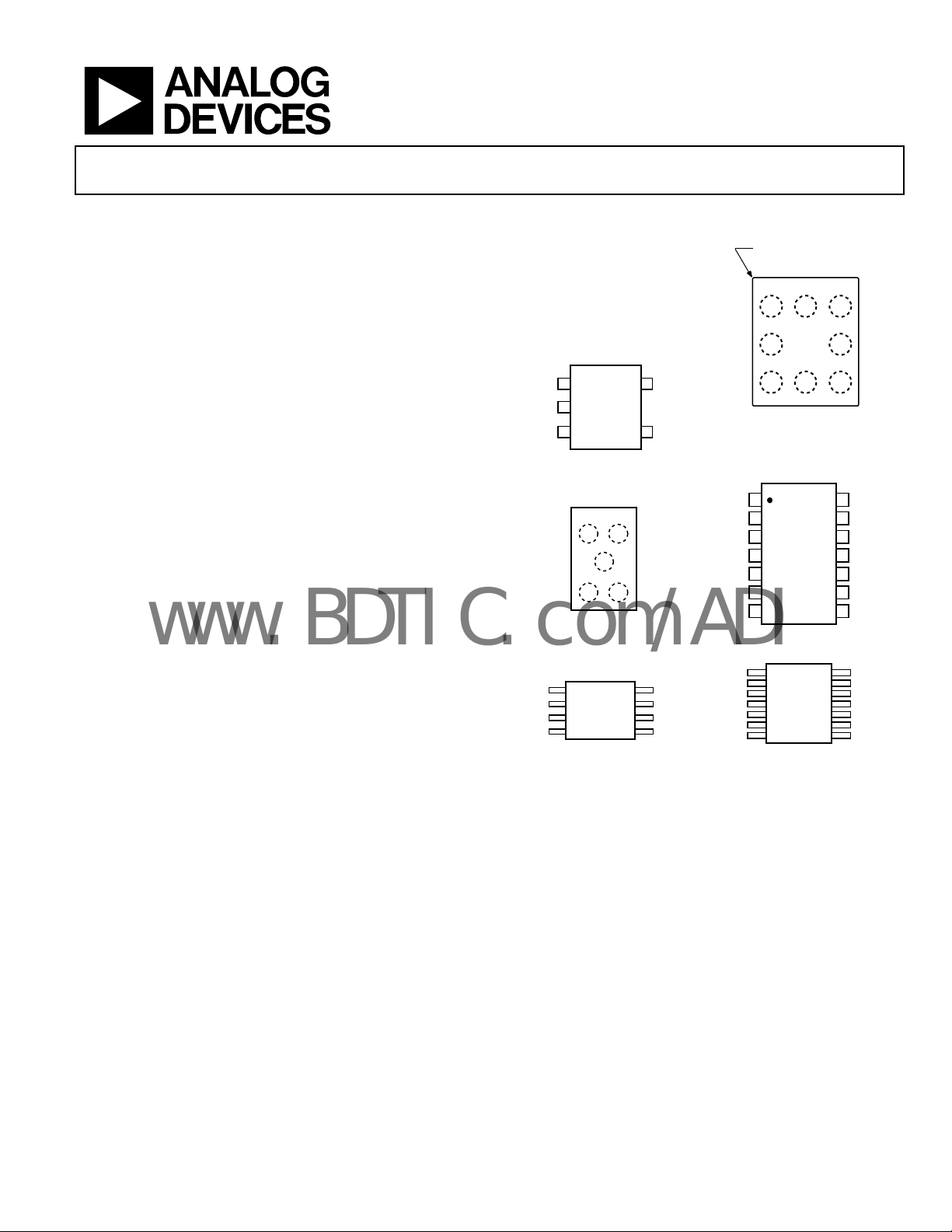
AD8605/AD8606/AD8608
FUNCTIONAL BLOCK DIAGRAMS
BALLA1
CORNER
OUTA V+ OUTB
A1 A2 A3
–INA –INB
B1 B3
+INA V– +INB
–IN A
+IN A
+IN B
–IN B
UT B
–IN A
+IN A
V+
+IN B
–IN B
UT B
V+
C1 C2 C3
AD8606
TOP VIEW
(BALL SIDE DO WN)
1
2
3
AD8608
TOP VIEW
4
(Not to Scal e)
5
6
7
1
(Not to Scale)
7
AD8608
TOP VIEW
14
OUT
+IN
V–
1
AD8605
TOP VIEW
2
(Not to Scale)
3
V+
5
–IN
4
2731-001
Figure 1. 5-Lead SOT-23 (RJ Suffix) Figure 2. 8-Ball WLCSP (CB Suffix)
TOP VIE W
(BUMP SIDE DO WN)
OUT V+
135
V–
2
+IN –IN
4
AD8605 ONLY
02731-006
OUT A
Figure 3. 5-Ball WLCSP (CB Suffix) Figure 4. 14-Lead SOIC_N (R Suffix)
18
UT A
–IN A
+IN A
AD8606
TOP VIEW
(Not to Scale)
45
V–
V+
OUT B
–IN B
+IN B
Figure 5. 8-Lead MSOP (RM Suffix),
OUT A
02731-003
Figure 6. 14-Lead TSSOP (RU Suffix)
8-Lead SOIC_N (R Suffix)
One Technology Way, P.O. Box 9106, Norwood, MA 02062-9106, U.S.A.
Tel: 781.329.4700 www.analog.com
Fax: 781.461.3113 ©2002–2008 Analog Devices, Inc. All rights reserved.
02731-057
14
OUT D
13
–IN D
12
+IN D
11
V–
10
+IN C
9
–IN C
8
OUT C
02731-004
OUT D
–IN D
+IN D
V–
+IN C
–IN C
8
OUT C
02731-002
Page 2

AD8605/AD8606/AD8608
www.BDTIC.com/ADI
TABLE OF CONTENTS
Features .............................................................................................. 1
Applications ....................................................................................... 1
General Description ......................................................................... 1
Functional Block Diagrams ............................................................. 1
Revision History ............................................................................... 3
5 V Electrical Specifications ............................................................ 4
2.7 V Electrical Specifications ......................................................... 6
Absolute Maximum Ratings ............................................................ 8
ESD Caution .................................................................................. 8
Typical Performance Characteristics ............................................. 9
Applications Information .............................................................. 15
Output Phase Reversal ............................................................... 15
Maximum Power Dissipation ................................................... 15
Input Overvoltage Protection ................................................... 15
THD + Noise ............................................................................... 15
Total Noise Including Source Resistors ................................... 16
Channel Separation .................................................................... 16
Capacitive Load Drive ............................................................... 16
Light Sensitivity .......................................................................... 17
WLCSP Assembly Considerations ........................................... 17
I-V Conversion Applications ........................................................ 18
Photodiode Preamplifier Applications .................................... 18
Audio and PDA Applications ................................................... 18
Instrumentation Amplifiers ...................................................... 19
DAC Conversion ........................................................................ 19
Outline Dimensions ....................................................................... 20
Ordering Guide .......................................................................... 22
Rev. I | Page 2 of 24
Page 3

AD8605/AD8606/AD8608
www.BDTIC.com/ADI
REVISION HISTORY
9/08—Rev. H to Rev. I
Changes to Input Overvoltage Protection Section ................ 15
Changes to Ordering Guide ...................................................... 22
2/08—Rev. G to Rev. H
Changes to Features ..................................................................... 1
Changes to Table 1 ....................................................................... 4
Changes to Table 2 ....................................................................... 6
Changes to Figure 11 ................................................................... 9
Changes to Figure 13, Figure 14, and Figure 16 Captions .... 10
Changes to Figure 15, Figure 17, and Figure 18 ..................... 10
Changes to Figure 34 and Figure 35 Captions ........................ 13
Changes to Figure 36 ................................................................. 13
Changes to Figure 37 Caption .................................................. 14
Changes to Figure 38 and Figure 41 ........................................ 14
Changes to Figure 45 ................................................................. 15
Changes to Audio and PDA Applications Section ................. 18
Changes to Figure 52 ................................................................. 18
Changes to Ordering Guide ...................................................... 22
10/07—Rev. F to Rev. G
Changes to Figure 2 ...................................................................... 1
Updated Outline Dimensions ................................................... 20
8/07—Rev. E to Rev. F
Added 8-Ball WLCSP Package ..................................... Universal
Changes to Features ..................................................................... 1
Changes to Table 1 ....................................................................... 3
Changes to Table 2 ....................................................................... 5
Changes to Table 4 ....................................................................... 7
Updated Outline Dimensions ................................................... 19
Changes to Ordering Guide ...................................................... 21
1/06—Rev. D to Rev. E
Changes to Table 1 ....................................................................... 3
Changes to Table 2 ....................................................................... 5
Changes to Table 4 ....................................................................... 6
Changes to Figure 12 Caption .................................................... 8
Changes to Figure 26 and Figure 27 Captions ........................ 11
Changes to Figure 33 Caption .................................................. 12
Changes to Figure 44 ................................................................. 14
Updated Outline Dimensions ................................................... 19
Changes to Ordering Guide ...................................................... 20
5/04—Rev. C to Rev. D
Updated Format ............................................................. Universal
Edit to Light Sensitivity Section ............................................... 16
Updated Outline Dimensions ................................................... 19
Changes to Ordering Guide ...................................................... 20
7/03—Rev. B to Rev. C
Changes to Features ....................................................................... 1
Change to General Description .................................................... 1
Addition to Functional Block Diagrams ..................................... 1
Addition to Absolute Maximum Ratings .................................... 4
Addition to Ordering Guide ......................................................... 4
Change to Equation in Maximum Power Dissipation
Section .......................................................................................... 11
Added Light Sensitivity Section ................................................ 12
Added New Figure 8; Renumbered Subsequently .................. 13
Added New MicroCSP Assembly Considerations Section .... 13
Changes to Figure 9 .................................................................... 13
Change to Equation in Photodiode Preamplifier
Applications Section .................................................................. 13
Changes to Figure 12 .................................................................. 14
Change to Equation in D/A Conversion Section .................... 14
Updated Outline Dimensions ................................................... 15
3/03—Rev. A to Rev. B
Changes to Functional Block Diagram ....................................... 1
Changes to Absolute Maximum Ratings..................................... 4
Changes to Ordering Guide ........................................................ 4
Changes to Figure 9 ................................................................... 13
Updated Outline Dimensions .................................................... 15
11/02—Rev. 0 to Rev. A
Change to Electrical Characteristics ............................................ 2
Changes to Absolute Maximum Ratings..................................... 4
Changes to Ordering Guide ......................................................... 4
Change to TPC 6 ........................................................................... 5
Updated Outline Dimensions .................................................... 15
5/02—Revision 0: Initial Version
Rev. I | Page 3 of 24
Page 4
AD8605/AD8606/AD8608
www.BDTIC.com/ADI
5 V ELECTRICAL SPECIFICATIONS
VS = 5 V, VCM = VS/2, TA = 25°C, unless otherwise noted.
Table 1.
Parameter Symbol Conditions Min Typ Max Unit
INPUT CHARACTERISTICS
Offset Voltage VOS
AD8605/AD8606 (Except WLCSP) VS = 3.5 V, VCM = 3 V 20 65 μV
AD8608 VS = 3.5 V, VCM = 2.7 V 20 75 μV
AD8605/AD8606/AD8608 VS = 5 V, VCM = 0 V to 5 V 80 300 μV
−40°C < TA < +125°C 750 μV
Input Bias Current IB 0.2 1 pA
AD8605/AD8606 −40°C < TA < +85°C 50 pA
AD8605/AD8606 −40°C < TA < +125°C 250 pA
AD8608 −40°C < TA < +85°C 100 pA
AD8608 −40°C < TA < +125°C 300 pA
Input Offset Current IOS 0.1 0.5 pA
−40°C < TA < +85°C 20 pA
−40°C < TA < +125°C 75 pA
Input Voltage Range 0 5 V
Common-Mode Rejection Ratio CMRR VCM = 0 V to 5 V 85 100 dB
−40°C < TA < +125°C 75 90 dB
Large Signal Voltage Gain AVO RL = 2 kΩ, VO = 0.5 V to 4.5 V 300 1000 V/mV
Offset Voltage Drift
AD8605/AD8606 ΔVOS/ΔT −40°C < TA < +125°C 1 4.5 μV/°C
AD8608 ΔVOS/ΔT −40°C < TA < +125°C 1.5 6.0 μV/°C
INPUT CAPACITANCE
Common-Mode Input Capacitance C
Differential Input Capacitance C
OUTPUT CHARACTERISTICS
Output Voltage High VOH IL = 1 mA 4.96 4.98 V
I
−40°C < TA < +125°C 4.6 V
Output Voltage Low VOL IL = 1 mA 20 40 mV
I
−40°C < TA < +125°C 290 mV
Output Current I
Closed-Loop Output Impedance Z
POWER SUPPLY
Power Supply Rejection Ratio PSRR
AD8605/AD8606 VS = 2.7 V to 5.5 V 80 95 dB
AD8605/AD8606 WLCSP VS = 2.7 V to 5.5 V 75 92 dB
AD8608 VS = 2.7 V to 5.5 V 77 92 dB
−40°C < TA < +125°C 70 90 dB
Supply Current/Amplifier ISY I
−40°C < TA < +125°C 1.4 mA
DYNAMIC PERFORMANCE
Slew Rate SR RL = 2 kΩ, CL = 16 pF 5 V/μs
Settling Time tS To 0.01%, 0 V to 2 V step, AV = 1 <1 μs
Unity Gain Bandwidth Product GBP 10 MHz
Phase Margin Φ
8.8 pF
COM
2.6 pF
DIFF
= 10 mA 4.7 4.79 V
L
= 10 mA 170 210 mV
L
±80 mA
OUT
f = 1 MHz, AV = 1 1 Ω
OUT
= 0 mA 1 1.2 mA
OUT
M
65 Degrees
Rev. I | Page 4 of 24
Page 5

AD8605/AD8606/AD8608
www.BDTIC.com/ADI
Parameter Symbol Conditions Min Typ Max Unit
NOISE PERFORMANCE
Peak-to-Peak Noise en p-p f = 0.1 Hz to 10 Hz 2.3 3.5 μV p-p
Voltage Noise Density en f = 1 kHz 8 12 nV/√Hz
e
Current Noise Density in f = 1 kHz 0.01 pA/√Hz
f = 10 kHz 6.5 nV/√Hz
n
Rev. I | Page 5 of 24
Page 6
AD8605/AD8606/AD8608
www.BDTIC.com/ADI
2.7 V ELECTRICAL SPECIFICATIONS
VS = 2.7 V, VCM = VS/2, TA = 25°C, unless otherwise noted.
Table 2.
Parameter Symbol Conditions Min Typ Max Unit
INPUT CHARACTERISTICS
Offset Voltage VOS
AD8605/AD8606 (Except WLCSP) VS = 3.5 V, VCM = 3 V 20 65 μV
AD8608 VS = 3.5 V, VCM = 2.7 V 20 75 μV
AD8605/AD8606/AD8608 VS = 2.7 V, VCM = 0 V to 2.7 V 80 300 μV
−40°C < TA < +125°C 750 μV
Input Bias Current IB 0.2 1 pA
AD8605/AD8606 −40°C < TA < +85°C 50 pA
AD8605/AD8606 −40°C < TA < +125°C 250 pA
AD8608 −40°C < TA < +85°C 100 pA
AD8608 −40°C < TA < +125°C 300 pA
Input Offset Current IOS 0.1 0.5 pA
−40°C < TA < +85°C 20 pA
−40°C < TA < +125°C 75 pA
Input Voltage Range 0 2.7 V
Common-Mode Rejection Ratio CMRR VCM = 0 V to 2.7 V 80 95 dB
−40°C < TA < +125°C 70 85 dB
Large Signal Voltage Gain AVO RL = 2 kΩ, VO = 0.5 V to 2.2 V 110 350 V/mV
Offset Voltage Drift
AD8605/AD8606 ΔVOS/ΔT −40°C < TA < +125°C 1 4.5 μV/°C
AD8608 ΔVOS/ΔT −40°C < TA < +125°C 1.5 6.0 μV/°C
INPUT CAPACITANCE
Common-Mode Input Capacitance C
Differential Input Capacitance C
OUTPUT CHARACTERISTICS
Output Voltage High VOH IL = 1 mA 2.6 2.66 V
−40°C < TA < +125°C 2.6 V
Output Voltage Low VOL IL = 1 mA 25 40 mV
−40°C < TA < +125°C 50 mV
Output Current I
Closed-Loop Output Impedance Z
POWER SUPPLY
Power Supply Rejection Ratio PSRR
AD8605/AD8606 VS = 2.7 V to 5.5 V 80 95 dB
AD8605/AD8606 WLCSP VS = 2.7 V to 5.5 V 75 92 dB
AD8608 VS = 2.7 V to 5.5 V 77 92 dB
−40°C < TA < +125°C 70 90 dB
Supply Current/Amplifier I
−40°C < TA < +125°C 1.5 mA
DYNAMIC PERFORMANCE
Slew Rate SR RL = 2 kΩ, CL = 16 pF 5 V/μs
Settling Time tS To 0.01%, 0 V to 1 V step, AV = 1 <0.5 μs
Unity Gain Bandwidth Product GBP 9 MHz
Phase Margin Φ
8.8 pF
COM
2.6 pF
DIFF
±30 mA
OUT
f = 1 MHz, AV = 1 1.2 Ω
OUT
I
SY
M
= 0 mA 1.15 1.4 mA
OUT
50 Degrees
Rev. I | Page 6 of 24
Page 7

AD8605/AD8606/AD8608
www.BDTIC.com/ADI
Parameter Symbol Conditions Min Typ Max Unit
NOISE PERFORMANCE
Peak-to-Peak Noise en p-p f = 0.1 Hz to 10 Hz 2.3 3.5 μV p-p
Voltage Noise Density en f = 1 kHz 8 12 nV/√Hz
e
Current Noise Density in f = 1 kHz 0.01 pA/√Hz
f = 10 kHz 6.5 nV/√Hz
n
Rev. I | Page 7 of 24
Page 8
AD8605/AD8606/AD8608
www.BDTIC.com/ADI
ABSOLUTE MAXIMUM RATINGS
Table 3.
Parameter Rating
Supply Voltage 6 V
Input Voltage GND to V
Differential Input Voltage 6 V
Output Short-Circuit Duration to GND Observe Derating Curves
Storage Temperature Range
All Packages −65°C to +150°C
Operating Temperature Range
All Packages −40°C to +125°C
Junction Temperature Range
All Packages −65°C to +150°C
Lead Temperature (Soldering, 60 sec) 300°C
Stresses above those listed under Absolute Maximum Ratings
may cause permanent damage to the device. This is a stress
rating only; functional operation of the device at these or any
other conditions above those indicated in the operational
section of this specification is not implied. Exposure to absolute
maximum rating conditions for extended periods may affect
device reliability.
S
Table 4.
Package Type θ
5-Ball WLCSP (CB) 170 °C/W
5-Lead SOT-23 (RJ) 240 92 °C/W
8-Ball WLCSP (CB) 115 °C/W
8-Lead MSOP (RM) 206 44 °C/W
8-Lead SOIC_N (R) 157 56 °C/W
14-Lead SOIC_N (R) 105 36 °C/W
14-Lead TSSOP (RU) 148 23 °C/W
1
θJA is specified for the worst-case conditions, that is, a device soldered in a
circuit board for surface-mount packages.
1
θJC Unit
JA
ESD CAUTION
Rev. I | Page 8 of 24
Page 9

AD8605/AD8606/AD8608
m
www.BDTIC.com/ADI
TYPICAL PERFORMANCE CHARACTERISTICS
4500
VS = 5V
T
= 25°C
4000
A
V
= 0V TO 5V
CM
3500
3000
2500
2000
1500
NUMBER OF AMPLIF IERS
1000
500
0
–300
OFFSET VOLTAGE (µV)
300–200 –100 0 100 200
Figure 7. Input Offset Voltage Distribution
24
20
16
12
8
NUMBER OF AMPLIFIERS
4
0
0.8 1.6 2.4 3.2 4.0
0 1.2 2.0 2.8 3.6
TCVOS (µV/° C)
VS = 5V
= –40°C TO +125° C
T
A
= 2.5V
V
CM
4.4
4.80.4
Figure 8. AD8608 Input Offset Voltage Drift Distribution
20
18
16
14
12
10
8
6
NUMBER OF AMPLIF IERS
4
2
0
0.4 0.6 0.8 1. 0 1.2 1.4 1.6 1.8 2.0
0
TCVOS (µV/° C)
Figure 9. AD8605/AD8606 Input Offset Voltage Drift Distribution
= 5V
V
S
T
= –40°C TO +125° C
A
V
= 2.5V
CM
2.2 2.4
2.60.2
02731-007
8
0
-0
1
3
7
2
0
02731-009
0.30
0.25
0.20
0.15
0.10
0.05
V)
(
0
OS
V
–0.05
–0.10
–0.15
–0.20
–0.25
–0.30
0 0.5 1.0 1.5 2.0 2.5 3.0 3.5 4.0 4.5 5.0
V
(V)
CM
Figure 10. Input Offset Voltage vs. Common-Mode Voltage
(200 Units, 5 Wafer Lots, Including Process Skews)
360
VS = ±5V
320
280
240
200
160
120
INPUT BIAS CURRENT (pA)
80
40
0
0125
50 75 100
TEMPERATURE (°C)
AD8605/AD8606
AD8608
Figure 11. Input Bias Current vs. Temperature
1k
VS = 5V
= 25°C
T
A
100
10
SINKSOURCE
1
OUTPUT SATURATION VOLTAGE (mV)
0.1
0.001 100.01
Figure 12. Output Saturation Voltage vs. Load Current
0.1
LOAD CURRENT (mA)
1
02731-010
02731-011
25
02731-012
Rev. I | Page 9 of 24
Page 10

AD8605/AD8606/AD8608
T
www.BDTIC.com/ADI
5.00
6
4.95
= 5V
V
S
4.90
4.85
4.80
OUTPUT VOLTAGE (V)
4.75
4.70
–40 –25 –10 5 20 35 50 65 80 95 110 125
V
@ 10mA LOAD
OH
TEMPERATURE (°C)
VOH @ 1mA LOAD
Figure 13. Output Voltage Swing High vs. Temperature
0.25
= 5V
V
S
0.20
0.15
AGE (V)
0.10
OUTPUT VOL
0.05
0
–40 –25 –10 5 20 35 50 65 80 95 110 125
TEMPERATURE (°C)
V
@ 10mA LOAD
OL
VOL @ 1mA LOAD
Figure 14. Output Voltage Swing Low vs. Temperature
100
80
60
40
20
0
GAIN (dB)
–20
–40
–60
–80
–100
10k 40M100k 1M 10M
FREQUENCY ( Hz)
Figure 15. Open-Loop Gain and Phase vs. Frequency
V
R
C
Φ
= ±2.5V
S
= 2kΩ
L
= 20pF
L
= 64°
M
225
180
135
90
45
0
–45
–90
–135
–180
–225
5
VS = 5V
4
V
= 4.9V p-p
IN
T
= 25°C
A
R
= 2kΩ
L
3
A
= 1
V
2
OUTPUT SWING (V p-p)
1
02731-013
0
1k 10M10k
100k 1M
FREQUENCY ( Hz)
02731-016
Figure 16. Closed-Loop Output Voltage Swing (FPBW)
100
VS = 5V
90
80
70
60
50
40
30
OUTPUT IMPEDANCE (Ω)
20
10
02731-014
0
1k 100M10k 100k 1M 10M
AV = 100
AV = 10
FREQUENCY (Hz)
AV = 1
02731-017
Figure 17. Output Impedance vs. Frequency
120
VS = 5V
110
100
90
80
70
CMRR (dB)
PHASE (Degrees)
02731-015
60
50
40
30
20
1k 10M
10k
100k 1M
FREQUENCY ( Hz)
Figure 18. Common-Mode Rejection Ratio (CMRR) vs. Frequency
02731-018
Rev. I | Page 10 of 24
Page 11

AD8605/AD8606/AD8608
A
T
www.BDTIC.com/ADI
140
VS = 5V
120
100
80
60
40
PSRR (dB)
20
0
–20
–40
–60
1k 10M10k
Figure 19. PSRR vs. Frequency
45
VS = 5V
40
R
=
∞
L
TA = 25°C
35
A
= 1
V
30
25
L OVERSHOOT (%)
20
15
10
SMALL SIGN
5
0
10 1k100
CAPACITANCE (pF)
100k 1M
02731-019
FREQUENCY (Hz)
+OS
–OS
02731-020
1.0
0.9
0.8
0.7
0.6
0.5
0.4
0.3
0.2
SUPPLY CURRENT/AMPLIFI ER (mA)
0.1
0
054.54.03.53.02.52.01.51.00.5
SUPPLY VOLTAGE (V)
Figure 22. Supply Current/Amplifier vs. Supply Voltage
VS = 5V
AGE NOISE (1µV/DIV)
VOL
TIME (1s/ DIV)
02731-022
.0
02731-023
Figure 20. Small Signal Overshoot vs. Load Capacitance
2.0
1.5
VS = 2.7V
1.0
0.5
SUPPLY CURRENT/AMPLIFI ER (mA)
0
–40 125–25 –10 95 110
52035506580
Figure 21. Supply Current/Amplifier vs. Temperature
= 5V
V
S
TEMPERATURE (°C)
02731-021
Rev. I | Page 11 of 24
Figure 23. 0.1 Hz to 10 Hz Input Voltage Noise
VS = ±2.5V
= 10kΩ
R
L
= 200pF
C
L
= 1
A
V
VOLTAGE (50mV/DIV)
TIME (200n s/DIV)
Figure 24. Small Signal Transient Response
02731-024
Page 12

AD8605/AD8606/AD8608
V
T
www.BDTIC.com/ADI
VS = ±2.5V
R
= 10kΩ
L
C
= 200pF
L
A
= 1
V
36
VS = ±2.5V
32
28
24
20
OUT
V
VOLTAGE (1V/DIV)
TIME (400ns/DIV)
Figure 25. Large Signal Transient Response
2.5V
0V
0V
IN
–50mV
TIME (400ns/DIV)
VS = ±2.5V
R
= 10kΩ
L
A
= –100
V
V
= 50mV
IN
16
12
VOLTAGE NOISE DENSITY (nV/ Hz)
8
02731-025
4
010.90.80. 70.60.50.40. 30.20.1
FREQUE NCY (kHz )
02731-028
.0
Figure 28. Voltage Noise Density vs. Frequency
53.6
VS = ±2.5V
46.9
40.2
33.5
26.8
20.1
AGE NOISE DENSITY (nV/ Hz)
13.4
VOL
6.7
02731-026
0
01987654321
FREQUE NCY (kHz )
02731-029
0
0V
–2.5V
50mV
0V
Figure 26. Positive Overload Recovery
VS = ±2.5V
R
= 10kΩ
L
A
= –100
V
V
= 50mV
IN
TIME (1µs/DIV)
Figure 27. Negative Overload Recovery
02731-027
Figure 29. Voltage Noise Density vs. Frequency
119.2
VS = ±2.5V
104.3
89.4
74.5
59.6
44.7
29.8
VOLTAGE NOISE DENSITY (nV/ Hz)
14.9
0
0 100908070605040302010
FREQUENCY (Hz)
Figure 30. Voltage Noise Density vs. Frequency
02731-030
Rev. I | Page 12 of 24
Page 13

AD8605/AD8606/AD8608
A
A
www.BDTIC.com/ADI
1800
VS = 2.7V
T
800
600
400
200
0
–300
= 25°C
A
V
= 0V TO 2.7V
CM
OFFSET VOLTAGE (µV)
0100
1600
1400
1200
1000
NUMBER OF AMPLIFIERS
Figure 31. Input Offset Voltage Distribution
300
VS = 2.7V
T
= 25°C
A
200
100
0
–100
INPUT OFFSET VOLTAGE (µV)
–200
–300
0
COMMON-MODE VOLTAGE (V)
Figure 32. Input Offset Voltage vs. Common-Mode Voltage
(200 Units, 5 Wafer Lots, Including Process Skews)
1k
VS = 2.7V
T
= 25°C
A
100
SOURCE
10
TION VOLTAGE (mV)
TUR
1
OUTPUT S
0.1
0.001 100.01
0.1
LOAD CURRENT (mA)
Figure 33. Output Saturation Voltage vs. Load Current
1.80.90
SINK
1
02731-031
300–200 –100 200
02731-032
2.7
02731-033
OU T PU T V OLTA G E ( V)
2.680
2.675
2.670
2.665
2.660
2.655
2.650
VS = 2.7V
–10–25–40
VOH @ 1mA LOAD
5 20 1255035
TEMPERATURE (°C)
65 80 95 110
Figure 34. Output Voltage Swing High vs. Temperature
OUTPUT VOLTAGE (V)
0.045
0.040
0.035
0.030
0.025
0.020
0.015
0.010
0.005
VS = 2.7V
VOL @ 1mA LOAD
0
520 1255035
TEMPERATURE (°C)
65 80 95 110–10–25–40
Figure 35. Output Voltage Swing Low vs. Temperature
100
80
60
40
20
0
GAIN (dB)
–20
–40
–60
–80
–100
10k 40M100k
FREQUENCY ( Hz)
1M 10M
Figure 36. Open-Loop Gain and Phase vs. Frequency
VS = 2.7V
R
= 2kΩ
L
C
= 20pF
L
Φ
= 52.5°
M
225
180
135
90
45
0
–45
–90
–135
–180
–225
02731-034
02731-035
PHASE (Degrees)
02731-036
Rev. I | Page 13 of 24
Page 14

AD8605/AD8606/AD8608
A
A
T
www.BDTIC.com/ADI
3.0
2.5
2.0
1.5
1.0
OUTPUT SWING (V p-p)
0.5
VS = 2.7V
= 2.6V p-p
V
IN
= 25°C
T
A
= 2kΩ
R
L
= 1
A
V
VS = 2.7V
VOLTAGE NOISE (1µV/DIV)
0
1k 10M10k
100k 1M
FREQUENCY ( Hz)
Figure 37. Closed-Loop Output Voltage Swing vs. Frequency (FPBW)
100
VS = 2.7V
90
80
70
60
50
40
30
OUTPUT IMPEDANCE (Ω)
20
10
0
1k
AV = 100
AV = 10
AV = 1
100M10k 100k 1M 10M
FREQUENCY ( Hz)
Figure 38. Output Impedance vs. Frequency
60
VS = 2.7V
T
= 25°C
A
50
A
= 1
V
40
–OS
+OS
L OVERSHOOT (%)
LL SIGN
SM
30
20
10
02731-037
TIME (1s/ DIV)
02731-040
Figure 40. 0.1 Hz to 10 Hz Input Voltage Noise
VS = ±1.35V
R
= 10kΩ
L
C
= 200pF
L
A
= 1
V
VOLTAGE (50mV/DIV)
02731-038
TIME (200n s/DIV)
02731-041
Figure 41. Small Signal Transient Response
VS = 1.35V
R
= 10kΩ
L
C
= 200pF
L
A
= 1
V
AGE (1V/DIV)
VOL
0
10 1k100
CAPACITANCE (pF)
Figure 39. Small Signal Overshoot vs. Load Capacitance
02731-039
TIME (400n s/DIV)
Figure 42. Large Signal Transient Response
Rev. I | Page 14 of 24
02731-042
Page 15

AD8605/AD8606/AD8608
A
www.BDTIC.com/ADI
APPLICATIONS INFORMATION
OUTPUT PHASE REVERSAL
Phase reversal is defined as a change in polarity at the output of
the amplifier when a voltage that exceeds the maximum input
common-mode voltage drives the input.
Phase reversal can cause permanent damage to the amplifier; it
can also cause system lockups in feedback loops. The AD8605
does not exhibit phase reversal even for inputs exceeding the
supply voltage by more than 2 V.
MAXIMUM POWER DISSIPATION
Power dissipated in an IC causes the die temperature to
increase, which can affect the behavior of the IC and the
application circuit performance.
The absolute maximum junction temperature of the AD8605/
AD8606/AD8608 is 150°C. Exceeding this temperature could
damage or destroy the device.
The maximum power dissipation of the amplifier is calculated
according to
TT
−
J
A
P
=
DISS
θ
JA
where:
T
is the junction temperature.
J
is the ambient temperature.
T
A
θ
is the junction-to-ambient thermal resistance.
JA
Figure 44 compares the maximum power dissipation with
temperature for the various AD860x family packages.
INPUT OVERVOLTAGE PROTECTION
The AD8605 has internal protective circuitry. However, if the
voltage applied at either input exceeds the supplies by more
than 0.5 V, external resistors should be placed in series with
the inputs. The resistor values can be determined by
−
VV
IN
S
mA5≤
R
S
The remarkable low input offset current of the AD8605 (<1 pA)
allows the use of larger value resistors. With a 10 kΩ resistor at
the input, the output voltage has less than 10 nV of error voltage.
A 10 kΩ resistor has less than 13 nV/√Hz of thermal noise at
room temperature.
THD + NOISE
Total harmonic distortion is the ratio of the input signal in V rms
to the total harmonics in V rms throughout the spectrum.
Harmonic distortion adds errors to precision measurements
and adds unpleasant sonic artifacts to audio systems.
The AD8605 has a low total harmonic distortion. Figure 45 shows
that the AD8605 has less than 0.005% or −86 dB of THD + N
over the entire audio frequency range. The AD8605 is configured
in positive unity gain, which is the worst case, and with a load
of 10 kΩ.
Rev. I | Page 15 of 24
VS = ±2.5V
V
= 6V p-p
IN
A
= 1
V
R
= 10kΩ
L
VOLTAGE (2V/DIV)
V
IN
V
OUT
TIME (4µs/DIV)
Figure 43. No Phase Reversal
1.8
1.7
1.6
1.5
1.4
1.3
1.2
1.1
TION (W)
1.0
0.9
0.8
0.7
0.6
0.5
POWER DISSIP
0.4
0.3
0.2
0.1
0
–45 130–20
TSSOP-14
SOIC-8
MSOP-8
SOIC-14
WLCSP-5
5-LEAD SOT-23
555
30 80 105
AMBIENT TEMP ERATURE (° C)
Figure 44. Maximum Power Dissipation vs. Ambient Temperature
0.1
VSY = ±2.5V
A
= 1
V
B
= 80kHz
W
0.01
THD + NOISE (%)
0.001
0.0001
20 20k100
FREQUENCY ( Hz)
1k
10k
Figure 45. THD + Noise vs. Frequency
02731-043
02731-044
02731-045
Page 16

AD8605/AD8606/AD8608
(
)
A
V
www.BDTIC.com/ADI
TOTAL NOISE INCLUDING SOURCE RESISTORS
The low input current noise and input bias current of the
AD8605 make it the ideal amplifier for circuits with substantial
input source resistance, such as photodiodes. Input offset voltage
increases by less than 0.5 nV per 1 kΩ of source resistance at
room temperature and increases to 10 nV at 85°C. The total
noise density of the circuit is
n
,
TOTAL
2
2
()
nn
TRkRiee 4
++=
SS
where:
e
is the input voltage noise density of the AD8605.
n
i
is the input current noise density of the AD8605.
n
is the source resistance at the noninverting terminal.
R
S
k is Boltzmann’s constant (1.38 × 10
−23
J/K).
T is the ambient temperature in Kelvin (T = 273 + °C).
For example, with R
= 10 kΩ, the total voltage noise density is
S
roughly 15 nV/√Hz.
For R
< 3.9 kΩ, en dominates and e
S
n, TOTAL
≈ en.
The current noise of the AD8605 is so low that its total density does
not become a significant term unless R
is greater than 6 MΩ.
S
The total equivalent rms noise over a specific bandwidth is
expressed as
=
where
BW is the bandwidth in hertz.
BWeE
TOTALnn,
Note that the previous analysis is valid for frequencies greater
than 100 Hz and assumes relatively flat noise, above 10 kHz. For
lower frequencies, flicker noise (1/f) must be considered.
CHANNEL SEPARATION
Channel separation, or inverse crosstalk, is a measure of the signal
feed from one amplifier (channel) to another on the same IC.
The AD8606 has a channel separation of greater than −160 dB
up to frequencies of 1 MHz, allowing the two amplifiers to
amplify ac signals independently in most applications.
CAPACITIVE LOAD DRIVE
The AD860x can drive large capacitive loads without oscillation.
Figure 47 shows the output of the AD8606 in response to a
200 mV input signal. In this case, the amplifier is configured
in positive unity gain, worst case for stability, while driving a
1000 pF load at its output. Driving larger capacitive loads in
unity gain can require the use of additional circuitry.
A snubber network, shown in Figure 48, helps reduce the signal
overshoot to a minimum and maintain stability. Although this
circuit does not recover the loss of bandwidth induced by large
capacitive loads, it greatly reduces the overshoot and ringing.
This method does not reduce the maximum output swing of the
amplifier.
0
–20
–40
–60
TION (dB)
–80
–100
–120
CHANNEL SEPAR
–140
–160
–180
FREQUENCY (Hz)
Figure 46. Channel Separation vs. Frequency
10M1M100k10k1k100 100M
02731-046
VS = ±2.5V
A
= 1
V
R
= 10kΩ
L
C
= 1000pF
L
VOLTAGE (100mV/DIV)
TIME (10µ s/DIV)
Figure 47. AD8606 Capacitive Load Drive Without Snubber
02731-047
+
4
200mV
V
IN
2
AD8605
3
8
V–
Figure 48. Snubber Network Configuration
1
R
S
C
S
RLC
L
02731-049
Rev. I | Page 16 of 24
Page 17

AD8605/AD8606/AD8608
T
A
www.BDTIC.com/ADI
Figure 49 shows a scope of the output at the snubber circuit.
The overshoot is reduced from over 70% to less than 5%, and
the ringing is eliminated by the snubber. Optimum values for R
and C
are determined experimentally.
S
VS = ±2.5V
A
= 1
V
R
= 10kΩ
L
R
= 90Ω
S
C
= 1000pF
L
C
= 700pF
S
GE (100mV/DI V)
VOL
TIME (10µ s/DIV)
Figure 49. Capacitive Load Drive with Snubber
02731-048
Table 5 summarizes a few optimum values for capacitive loads.
Table 5.
CL (pF) RS (Ω) CS (pF)
500 100 1000
1000 70 1000
2000 60 800
An alternate technique is to insert a series resistor inside the
feedback loop at the output of the amplifier. Typically, the value
of this resistor is approximately 100 Ω. This method also reduces
overshoot and ringing but causes a reduction in the maximum
output swing.
LIGHT SENSITIVITY
The AD8605ACB (WLCSP package option) is essentially a
silicon die with additional postfabrication dielectric and
intermetallic processing designed to contact solder bumps
on the active side of the chip. With this package type, the die
is exposed to ambient light and is subject to photoelectric
effects. Light sensitivity analysis of the AD8605ACB mounted
on standard PCB material reveals that only the input bias
current (I
illuminated directly by high intensity light. No degradation in
electrical performance is observed due to illumination by low
intensity (0.1 mW/cm
increases with increasing wavelength and intensity of incident
light; I
3 mW/cm
shown in Figure 50 are not normal for most applications, that is,
even though direct sunlight can have intensities of 50 mW/cm
office ambient light can be as low as 0.1 mW/cm
) parameter is impacted when the package is
B
2
) ambient light. Figure 50 shows that IB
can reach levels as high as 4500 pA at a light intensity of
B
2
and a wavelength of 850 nm. The light intensities
2
.
2
5000
4500
S
4000
3500
3000
2500
2000
1500
INPUT BIAS CURRENT (pA)
1000
500
0
350
450 550 650 750 850
WAVELENGTH (nm)
Figure 50. AD8605ACB Input Bias Current Response to Direct Illumination of
Varying Intensity and Wavelength
2mW/cm
3mW/cm
2
2
1mW/cm
2
02731-050
When the WLCSP package is assembled on the board with the
bump side of the die facing the PCB, reflected light from the
PCB surface is incident on active silicon circuit areas and results
in the increased I
. No performance degradation occurs due to
B
illumination of the backside (substrate) of the AD8605ACB.
The AD8605ACB is particularly sensitive to incident light with
wavelengths in the near infrared range (NIR, 700 nm to 1000 nm).
Photons in this waveband have a longer wavelength and lower
energy than photons in the visible (400 nm to 700 nm) and near
ultraviolet (NUV, 200 nm to 400 nm) bands; therefore, they can
penetrate more deeply into the active silicon. Incident light with
wavelengths greater than 1100 nm has no photoelectric effect
on the AD8605ACB because silicon is transparent to wavelengths
in this range. The spectral content of conventional light sources
varies. Sunlight has a broad spectral range, with peak intensity
in the visible band that falls off in the NUV and NIR bands;
fluorescent lamps have significant peaks in the visible but not
the NUV or NIR bands.
Efforts have been made at a product level to reduce the effect of
ambient light; the under bump metal (UBM) has been designed
to shield the sensitive circuit areas on the active side (bump
side) of the die. However, if an application encounters any light
sensitivity with the AD8605ACB, shielding the bump side of the
WLCSP package with opaque material should eliminate this
effect. Shielding can be accomplished using materials such as
silica-filled liquid epoxies that are used in flip-chip underfill
techniques.
WLCSP ASSEMBLY CONSIDERATIONS
For detailed information on the WLCSP PCB assembly and
reliability, see Application Note AN-617,
,
Level Chip Scale Package
.
MicroCSP™ Wafer
Rev. I | Page 17 of 24
Page 18

AD8605/AD8606/AD8608
V
www.BDTIC.com/ADI
I-V CONVERSION APPLICATIONS
PHOTODIODE PREAMPLIFIER APPLICATIONS
The low offset voltage and input current of the AD8605 make
it an excellent choice for photodiode applications. In addition,
the low voltage and current noise make the amplifier ideal for
application circuits with high sensitivity.
C
F
10pF
R
F
10MΩ
PHOTODIODE
C
R
D
D
I
D
50pF
Figure 51. Equivalent Circuit for Photodiode Preamp
The input bias current of the amplifier contributes an error
term that is proportional to the value of R
The offset voltage causes a dark current induced by the shunt
resistance of the Diode R
. These error terms are combined at
D
the output of the amplifier. The error voltage is written as
⎞
R
F
⎟
+= 1
⎟
R
D
⎠
Typically, R
⎛
⎜
VE +
OSO
⎜
⎝
is smaller than RD, thus RF/RD can be ignored.
F
V
OS
AD8605
.
F
IR
BF
V
OUT
02731-051
At room temperature, the AD8605 has an input bias current of
0.2 pA and an offset voltage of 100 μV. Typical values of R
in the range of 1 GΩ.
For the circuit shown in Figure 51, the output error voltage is
approximately 100 μV at room temperature, increasing to about
1 mV at 85°C.
The maximum achievable signal bandwidth is
f
f
=
MAX
is the unity gain frequency of the amplifier.
where f
t
t
CR
π
2
FF
AUDIO AND PDA APPLICATIONS
The low distortion and wide dynamic range of the AD860x
make it a great choice for audio and PDA applications,
including microphone amplification and line output buffering.
Figure 52 shows a typical application circuit for headphone/
line-out amplification.
R1 and R2 are used to bias the input voltage at half the supply,
which maximizes the signal bandwidth range. C1 and C2 are
used to ac couple the input signal. C1, R1, and R2 form a highpass filter whose corner frequency is 1/[2π(R1||R2)C1].
The high output current of the AD8606 allows it to drive heavy
resistive loads.
The circuit in Figure 52 is tested to drive a 16 Ω headphone. The
THD + N is maintained at approximately −60 dB throughout the
audio range.
5
D
are
R1
C1
1µF
V1
500mV
C2
1µF
V2
500mV
20kΩ
20kΩ
20kΩ
20kΩ
R2
R7
R8
3
2
5
6
8
1/2
AD8606
4
5V
8
1/2
AD8606
4
C3
100µF
1
100µF
7
R4
20Ω
R3
HEADPHONES
1kΩ
C4
R6
20Ω
R5
1kΩ
02731-052
Figure 52. Single-Supply Headphone/Speaker Amplifier
Rev. I | Page 18 of 24
Page 19

AD8605/AD8606/AD8608
V
www.BDTIC.com/ADI
INSTRUMENTATION AMPLIFIERS
The low offset voltage and low noise of the AD8605 make it an
ideal amplifier for instrumentation applications.
Difference amplifiers are widely used in high accuracy circuits
to improve the common-mode rejection ratio. Figure 53 shows
a simple difference amplifier. Figure 54 shows the commonmode rejection for a unity gain configuration and for a gain of 10.
Making (R4/R3) = (R2/R1) and choosing 0.01% tolerance yields
a CMRR of 74 dB and minimizes the gain error at the output.
R1
V1
R4R3R2
=
V
OUT
V2
1kΩ
R1
R2
= (V2 – V1)
R1
R3
1kΩ
Figure 53. Difference Amplifier, A
120
VSY = ±2.5V
100
80
60
CMRR (dB)
40
20
0
100 10M1k
AV = 10
AV = 1
10k 100k 1M
FREQUENCY (Hz)
Figure 54. Difference Amplifier CMRR vs. Frequency
5V
AD8605
R2
10kΩ
R4
10kΩ
= 10
V
V
OUT
02731-053
02731-054
DAC CONVERSION
The low input bias current and offset voltage of the AD8605
make it an excellent choice for buffering the output of a current
output DAC.
Figure 55 shows a typical implementation of the AD8605 at the
output of a 12-bit DAC.
The DAC8143 output current is converted to a voltage by the
feedback resistor. The equivalent resistance at the output of the
DAC varies with the input code, as does the output capacitance.
V
REF
Figure 55. Simplified Circuit of the DAC8143 with AD8605 Output Buffer
To optimize the performance of the DAC, insert a capacitor in
the feedback loop of the AD8605 to compensate the amplifier
for the pole introduced by the output capacitance of the DAC.
Typical valu es for C
adjusted for the best frequency response. The total error at the
output of the op amp can be computed by
where Req is the equivalent resistance seen at the output of the
DAC. As previously mentioned, Req is code dependent and
varies with the input. A typical value for Req is 15 kΩ.
Choosing a feedback resistor of 10 kΩ yields an error of less
than 200 μV.
Figure 56 shows the implementation of a dual-stage buffer
at the output of a DAC. The first stage is used as a buffer.
Capacitor C1 with Req creates a low-pass filter, and thus,
provides phase lead to compensate for frequency response.
The second stage of the AD8606 is used to provide voltage
gain at the output of the buffer.
Grounding the positive input terminals in both stages reduces
errors due to the common-mode output voltage. Choosing R1,
R2, and R3 to match within 0.01% yields a CMRR of 74 dB and
maintains minimum gain error in the circuit.
IN
RRR
R2
R2 R2
V
C
F
R
F
V+
OS
AD8605
V–
range from 10 pF to 30 pF; it can be
F
+=
DB11
⎞
R
F
⎟
⎟
1Req
⎠
R
CS
C1
R
FB
OUT1
AGND
33pF
1/2
AD8606
R4
5kΩ
R1
10kΩ
R3
20kΩ
R2
10kΩ
1/2
AD8606
V
OUT
⎛
⎜
VE
OSO
⎜
⎝
15V
V
DD
AD7545
V
REF
R
P
Figure 56. Bipolar Operation
02731-055
02731-056
Rev. I | Page 19 of 24
Page 20

AD8605/AD8606/AD8608
www.BDTIC.com/ADI
OUTLINE DIMENSIONS
0.50 REF
SEATING
PLANE
0.87
0.23
0.18
0.14
0.21
12
0.50
A
B
C
BALL 1
IDENTIFIER
0.94
0.90
0.86
1.33
1.29
1.25
0.37
0.36
0.35
TOP VIEW
(BALL SI DE DOWN)
0.17
0.14
0.12
0.50
BOTTOM VIEW
(BALL SIDE UP)
0.20
101607-A
Figure 57. 5-Ball Wafer Level Chip Scale Package [WLCSP]
(CB-5-1)
Dimensions shown in millimeters
2.90 BSC
1.60 BSC
1.30
1.15
0.90
0.15 MAX
5
123
PIN 1
COMPLIANT TO JEDEC STANDARDS MO-178-A A
1.90
BSC
0.50
0.30
4
0.95 BSC
2.80 BSC
1.45 MAX
SEATING
PLANE
0.22
0.08
10°
5°
0°
0.60
0.45
0.30
Figure 58. 5-Lead Small Outline Transistor Package [SOT-23]
(RJ-5)
Dimensions shown in millimeters
3.20
3.00
2.80
8
5
4
SEATING
PLANE
5.15
4.90
4.65
1.10 MAX
0.23
0.08
8°
0°
0.80
0.60
0.40
3.20
3.00
1
2.80
PIN 1
0.65 BSC
0.95
0.85
0.75
0.15
0.38
0.00
0.22
COPLANARITY
0.10
COMPLIANT TO JEDEC STANDARDS MO-187-AA
Figure 59. 8-Lead Mini Small Outline Package [MSOP]
(RM-8)
Dimensions shown in millimeters
Rev. I | Page 20 of 24
Page 21

AD8605/AD8606/AD8608
www.BDTIC.com/ADI
5.00 (0.1968)
4.80 (0.1890)
4.00 (0.1574)
3.80 (0.1497)
0.25 (0.0098)
0.10 (0.0040)
COPLANARITY
0.10
CONTROLL ING DIMENSI ONS ARE IN MILLIMETERS; INCH DI MENSIONS
(IN PARENTHESES) ARE ROUNDED-OFF MILLIMETER EQUIVALENTS FOR
REFERENCE ONLY AND ARE NOT APPROPRI ATE FOR USE IN DESIGN.
85
1
1.27 (0.0500)
SEATING
PLANE
COMPLIANT TO JEDEC STANDARDS MS-012-A A
BSC
6.20 (0.2441)
5.80 (0.2284)
4
1.75 (0.0688)
1.35 (0.0532)
0.51 (0.0201)
0.31 (0.0122)
8°
0°
0.25 (0.0098)
0.17 (0.0067)
0.50 (0.0196)
0.25 (0.0099)
1.27 (0.0500)
0.40 (0.0157)
45°
012407-A
Figure 60. 8-Lead Standard Small Outline Package [SOIC_N]
Narrow Body (R-8)
Dimensions shown in millimeters and (inches)
0.675
0.595
0.515
SEATING
PLANE
0.50
BALL PITCH
0.27
0.24
0.21
0.340
0.320
0.300
BOTTOM VIEW
(BALL SI DE UP)
123
A
B
C
090706-B
BALL 1
IDENTIFIER
1.480
1.430
1.380
TOP VIEW
(BALL SI DE DOWN)
1.825
1.775
1.725
0.380
0.355
0.330
Figure 61. 8-Ball Wafer Level Chip Scale Package [WLCSP]
(CB-8-1)
Dimensions shown in millimeters
8.75 (0.3445)
8.55 (0.3366)
BSC
8
7
6.20 (0.2441)
5.80 (0.2283)
1.75 (0.0689)
1.35 (0.0531)
SEATING
PLANE
8°
0°
0.25 (0.0098)
0.17 (0.0067)
0.50 (0.0197)
0.25 (0.0098)
1.27 (0.0500)
0.40 (0.0157)
4.00 (0.1575)
3.80 (0.1496)
0.25 (0.0098)
0.10 (0.0039)
COPLANARIT Y
0.10
CONTROLL ING DIMENSIONS ARE IN MILLIMETERS; INCH DI MENSIONS
(IN PARENTHESES) ARE ROUNDED-O FF MIL LIMETE R EQUIVALENTS FOR
REFERENCE ON LY AND ARE NOT APPROPRI ATE FOR USE IN DESIGN.
14
1
1.27 (0.0500)
0.51 (0.0201)
0.31 (0.0122)
COMPLIANT TO JEDEC STANDARDS MS-012-AB
Figure 62. 14-Lead Standard Small Outline Package [SOIC_N]
Narrow Body (R-14)
Dimensions shown in millimeters and (inches)
Rev. I | Page 21 of 24
45°
060606-A
Page 22

AD8605/AD8606/AD8608
www.BDTIC.com/ADI
4.50
4.40
4.30
PIN 1
1.05
1.00
0.80
0.15
0.05
COPLANARITY
0.10
5.10
5.00
4.90
14
1
0.65 BSC
0.30
0.19
8
6.40
BSC
7
1.20
0.20
MAX
0.09
SEATING
PLANE
COMPLIANT T O JEDEC STANDARDS MO- 153-AB-1
8°
0°
0.75
0.60
0.45
061908-A
Figure 63. 14-Lead Thin Shrink Small Outline Package [TSSOP]
(RU-14)
Dimensions shown in millimeters
ORDERING GUIDE
Model Temperature Range Package Description Package Option Branding
AD8605ACB-REEL −40°C to +125°C 5-Ball WLCSP CB-5-1 B3A
AD8605ACB-REEL7 −40°C to +125°C 5-Ball WLCSP CB-5-1 B3A
AD8605ACBZ-REEL
AD8605ACBZ-REEL7
AD8605ART-R2 −40°C to +125°C 5-Lead SOT-23 RJ-5 B3A
AD8605ART-REEL −40°C to +125°C 5-Lead SOT-23 RJ-5 B3A
AD8605ART-REEL7 −40°C to +125°C 5-Lead SOT-23 RJ-5 B3A
AD8605ARTZ-R2
AD8605ARTZ-REEL
AD8605ARTZ-REEL7
AD8606ARM-R2 −40°C to +125°C 8-Lead MSOP RM-8 B6A
AD8606ARM-REEL −40°C to +125°C 8-Lead MSOP RM-8 B6A
AD8606ARMZ
AD8606ARMZ-R2
AD8606ARMZ-REEL
AD8606AR −40°C to +125°C 8-Lead SOIC_N R-8
AD8606AR-REEL −40°C to +125°C 8-Lead SOIC_N R-8
AD8606AR-REEL7 −40°C to +125°C 8-Lead SOIC_N R-8
AD8606ARZ
AD8606ARZ-REEL
AD8606ARZ-REEL7
AD8606ACBZ-REEL
AD8606ACBZ-REEL7
AD8608AR −40°C to +125°C 14-Lead SOIC_N R-14
AD8608AR-REEL −40°C to +125°C 14-Lead SOIC_N R-14
AD8608AR-REEL7 −40°C to +125°C 14-Lead SOIC_N R-14
AD8608ARZ
AD8608ARZ-REEL
AD8608ARZ-REEL7
AD8608ARU −40°C to +125°C 14-Lead TSSOP RU-14
AD8608ARU-REEL −40°C to +125°C 14-Lead TSSOP RU-14
AD8608ARUZ
AD8608ARUZ-REEL
1
Z = RoHS Compliant Part, # denotes RoHS compliant product (except for CB-5-1) may be top or bottom marked.
1
−40°C to +125°C 5-Ball WLCSP CB-5-1 A1J
1
−40°C to +125°C 5-Ball WLCSP CB-5-1 A1J
1
−40°C to +125°C 5-Lead SOT-23 RJ-5 B3A#
1
−40°C to +125°C 5-Lead SOT-23 RJ-5 B3A#
1
−40°C to +125°C 5-Lead SOT-23 RJ-5 B3A#
1
−40°C to +125°C 8-Lead MSOP RM-8 B6A#
1
−40°C to +125°C 8-Lead MSOP RM-8 B6A#
1
−40°C to +125°C 8-Lead MSOP RM-8 B6A#
1
−40°C to +125°C 8-Lead SOIC_N R-8
1
−40°C to +125°C 8-Lead SOIC_N R-8
1
−40°C to +125°C 8-Lead SOIC_N R-8
1
−40°C to +125°C 8-Ball WLCSP CB-8-1 B6A#
1
−40°C to +125°C 8-Ball WLCSP CB-8-1 B6A#
1
−40°C to +125°C 14-Lead SOIC_N R-14
1
−40°C to +125°C 14-Lead SOIC_N R-14
1
−40°C to +125°C 14-Lead SOIC_N R-14
1
−40°C to +125°C 14-Lead TSSOP RU-14
1
−40°C to +125°C 14-Lead TSSOP RU-14
Rev. I | Page 22 of 24
Page 23

AD8605/AD8606/AD8608
www.BDTIC.com/ADI
NOTES
Rev. I | Page 23 of 24
Page 24

AD8605/AD8606/AD8608
www.BDTIC.com/ADI
NOTES
©2002–2008 Analog Devices, Inc. All rights reserved. Trademarks and
registered trademarks are the property of their respective owners.
D02731-0-9/08(I)
Rev. I | Page 24 of 24
 Loading...