

Page 1
Dual 7 ns
a
FEATURES
7 ns Propagation Delay
Single Supply Operation: +3 V to +10 V
Low Power
Symmetrical Layout
Latch Function
TSSOP Packages
APPLICATIONS
Clock Recovery and Clock Distribution
High Speed Data
Line Receivers
Phase Detectors
Digital Communications
I and Q Detection
High Speed Sampling
Upgrade for MAX912
Satellite Receivers
PCMCIA Cards
Wireless Data Links
Battery Operated Instrumentation
Single Supply Comparator
AD8598
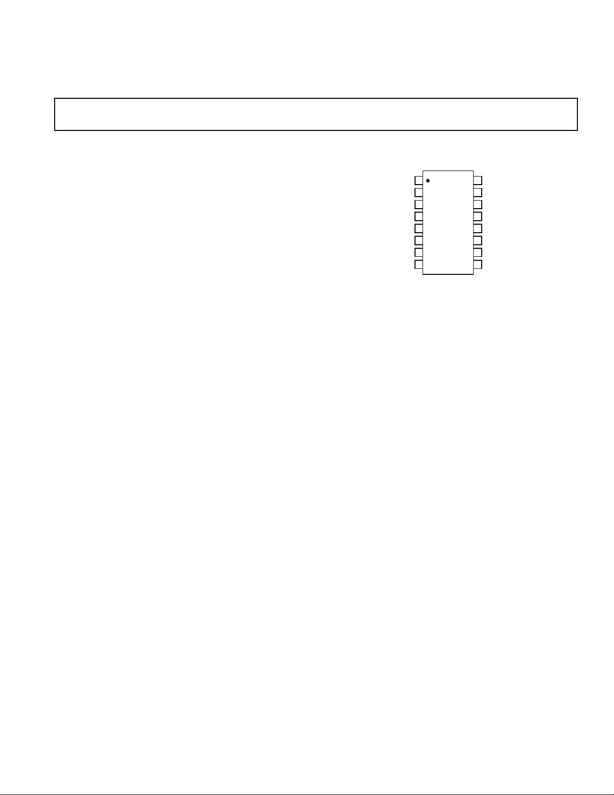
PIN CONFIGURATIONS
N-16, RU-16 and R-16A
1
QA
2
QA
3
GND
4
LEA
5
NC
6
V–
7
IN A–
8
IN A+
NC = NO CONNECT
AD8598
TOP VIEW
(Not to Scale)
16
QB
15
QB
14
GND
13
LEB
12
NC
11
V+
10
IN B–
9
IN B+
GENERAL DESCRIPTION
The AD8598 is a dual 7 ns comparator with digital latches.
Separate supplies enable the input stage to be operated from
+5 V to as high as ±5 V.
Ultrafast 7 ns propagation delay makes the AD8598 a good
choice for timing circuits and line receivers. Propagation delays
for rising and falling signals are closely matched and track over
temperature. This matched delay makes the AD8598 a good
choice for clock recovery, since the duty cycle of the output will
match the duty cycle of the input.
The AD8598 has the same pinout as the DIP version of the
AD9698. For a single comparator like the AD8598, please refer
to the AD8561 data sheet.
The AD8598 is specified over the industrial (–40°C to +85°C)
temperature range. The AD8598 is available in both the 16-lead
plastic DIP, 16-lead TSSOP or narrow R-16A surface mount
packages.
REV. A
Information furnished by Analog Devices is believed to be accurate and
reliable. However, no responsibility is assumed by Analog Devices for its
use, nor for any infringements of patents or other rights of third parties
which may result from its use. No license is granted by implication or
otherwise under any patent or patent rights of Analog Devices.
One Technology Way, P.O. Box 9106, Norwood, MA 02062-9106, U.S.A.
Tel: 781/329-4700 World Wide Web Site: http://www.analog.com
Fax: 781/326-8703 © Analog Devices, Inc., 1998
Page 2

AD8598–SPECIFICATIONS
ELECTRICAL SPECIFICATIONS
(@ V+ = +5.0 V, V– = V
= 0 V, TA = +25ⴗC unless otherwise noted)
GND
Parameter Symbol Conditions Min Typ Max Units
INPUT CHARACTERISTICS
Offset Voltage V
OS
–40°C ≤ T
Offset Voltage Drift ∆V
Input Bias Current I
Input Offset Current I
Input Common-Mode Voltage Range V
/∆T4µV/°C
OS
B
I
B
OS
CM
V
= 0 V –6 –3 µA
CM
–40°C ≤ TA ≤ +85°C –7 –3.5 µA
V
= 0 V ±4 µA
CM
Common-Mode Rejection Ratio CMRR 0 V ≤ V
R
Large Signal Voltage Gain A
Input Capacitance C
VO
IN
= 10 kΩ +3,000 V/V
L
≤ +85°C8mV
A
0.0 +3.0 V
≤ +3.0 V 65 85 dB
CM
2.3 7 mV
3.0 pF
LATCH ENABLE INPUT
Logic “1” Voltage Threshold V
Logic “0” Voltage Threshold V
Logic “1” Current I
Logic “0” Current I
IH
IL
IH
IL
V
= +3.0 V –1.0 –0.3 µA
LH
V
= +0.3 V –4 –2 µA
LL
+2.0 +1.65 V
+1.60 +0.8 V
Latch Enable
Pulsewidth t
Setup Time t
Hold Time t
PW(E)
S
H
6ns
1ns
1.2 ns
DIGITAL OUTPUTS
Logic “1” Voltage V
Logic “1” Voltage V
Logic “0” Voltage V
OH
OH
OL
I
= –50 µA, ∆V
OH
I
= –3.2 mA, ∆V
OH
I
= 3.2 mA, ∆V
OL
> 250 mV +3.5 V
IN
> 250 mV +2.4 +3.5 V
IN
> 250 mV +0.25 +0.4 V
IN
DYNAMIC PERFORMANCE␣
Propagation Delay t
Propagation Delay t
P
P
200 mV Step with 100 mV Overdrive 6.75 9.8 ns
–40°C ≤ T
≤ +85°C813ns
A
100 mV Step with 5 mV Overdrive 8 ns
Differential Propagation Delay
(Rising Propagation Delay vs.
Falling Propagation Delay) ∆t
P
100 mV Step with 100 mV Overdrive
1
0.5 2.0 ns
Rise Time 20% to 80% 3.8 ns
Fall Time 80% to 20% 1.5 ns
POWER SUPPLY␣
Power Supply Rejection Ratio PSRR +4.5 V ≤ V+ ≤ +5.5 V 50 65 dB
Positive Supply Current (V+ Pin) I+ 9.0 12.0 mA
Ground Supply Current (GND Pins) I
GND
–40°C ≤ T
VO = 0 V, RL =
–40°C ≤ T
≤ +85°C15.0mA
A
∞
≤ +85°C 7.6 mA
A
4.4 6.6 mA
Analog Supply Current (V– Pin) I– 4.6 9.0 mA
–40°C ≤ TA ≤ +85°C11.0mA
NOTES
1
Guaranteed by design.
Specifications subject to change without notice.
–2– REV. A
Page 3

AD8598
ELECTRICAL SPECIFICATIONS
(@ V+ = +5.0 V, V
= 0 V, V– = –5 V, TA = +25ⴗC unless otherwise noted)
GND
Parameter Symbol Conditions Min Typ Max Units
INPUT CHARACTERISTICS
Offset Voltage V
OS
–40°C ≤ T
Offset Voltage Drift ∆V
Input Bias Current I
Input Offset Current I
Input Common-Mode Voltage Range V
/∆T4µV/°C
OS
B
I
B
OS
CM
V
= 0 V –6 –3 µA
CM
–40°C ≤ TA ≤ +85°C –7 –2.5 µA
V
= 0 V ±4 µA
CM
Common-Mode Rejection Ratio CMRR –5.0 V ≤ V
R
Large Signal Voltage Gain A
Input Capacitance C
VO
IN
= 10 kΩ +3,000 V/V
L
≤ +85°C8mV
A
–5.0 +3.0 V
≤ +3.0 V 65 85 dB
CM
17 mV
3.0 pF
LATCH ENABLE INPUT
Logic “1” Voltage Threshold V
Logic “0” Voltage Threshold V
Logic “1” Current I
Logic “0” Current I
IH
IL
IH
IL
V
= +3.0 V –1 –0.5 µA
LH
V
= +0.3 V –4 –2 µA
LL
+2.0 +1.65 V
+1.60 +0.8 V
Latch Enable
Pulsewidth t
Setup Time t
Hold Time t
PW(E)
S
H
6ns
1.0 ns
1.2 ns
DIGITAL OUTPUTS
Logic “1” Voltage V
Logic “0” Voltage V
OH
OL
IOH = –3.2 mA +2.6 +3.5 V
IOL = 3.2 mA +0.2 +0.3 V
DYNAMIC PERFORMANCE␣
Propagation Delay t
Propagation Delay t
P
P
200 mV Step with 100 mV Overdrive 6.5 9.8 ns
–40°C ≤ T
≤ +85°C813ns
A
100 mV Step with 5 mV Overdrive 7 ns
Differential Propagation Delay
(Rising Propagation Delay vs.
Falling Propagation Delay) ∆t
P
100 mV Step with 100 mV Overdrive
1
0.5 2 ns
Rise Time 20% to 80% 3.8 ns
Fall Time 80% to 20% 1.5 ns
Dispersion 1ns
POWER SUPPLY
Power Supply Rejection Ratio PSRR ±4.5 V ≤ V
Supply Current V
= 0 V, RL =
O
and V
CC
≤ ±5.5 V 55 70 dB
EE
∞
Positive Supply Current (V+ Pin) I+ 9.4 13.0 mA
≤ +85°C 15.0 mA
A
∞
≤ +85°C 7.6 mA
A
4.4 6.6 mA
Ground Supply Current (GND Pins) I
GND
–40°C ≤ T
VO = 0 V, RL =
–40°C ≤ T
Analog Supply Current (V– Pin) I– 4.8 9.0 mA
–40°C ≤ TA ≤ +85°C 11.0 mA
NOTES
1
Guaranteed by design.
Specifications subject to change without notice.
–3–REV. A
Page 4
AD8598–SPECIFICATIONS
WARNING!
ESD SENSITIVE DEVICE
ELECTRICAL SPECIFICATIONS
(@ V+ = +3.0 V, V– = V
= 0 V, TA = +25ⴗC unless otherwise noted)
GND
Parameter Symbol Conditions Min Typ Max Units
INPUT CHARACTERISTICS␣
Offset Voltage V
Input Bias Current I
Input Common-Mode Voltage Range V
OS
B
I
B
CM
V
= 0 V –6 –3.0 µA
CM
–40°C ≤ TA ≤ +85°C–7–4µA
0 +1.5 V
7mV
Common-Mode Rejection Ratio CMRR +0.1 V ≤ VCM ≤ +1.5 V 50 dB
OUTPUT CHARACTERISTICS␣
Output High Voltage
Output Low Voltage V
1
V
OH
OL
IOH = –3.2 mA, VIN > 250 mV +1.2 V
IOL = +3.2 mA, VIN > 250 mV +0.3 V
POWER SUPPLY␣
Power Supply Rejection Ratio PSRR +2.7 V ≤ V
Supply Currents V
= 0 V, RL =
O
, V
≤ +6 V 40 dB
CC
EE
∞
Positive Supply Current (V+ Pin) I+ 8.0 9.0 mA
≤ +85°C11.0mA
A
3.2 5.0 mA
≤ +85°C 6.0 mA
A
Ground Supply Current (GND Pins) I
–40°C ≤ T
GND
–40°C ≤ T
Analog Supply Current (V– Pin) I– 4.8 6.6 mA
–40°C ≤ TA ≤ +85°C 7.6 mA
DYNAMIC PERFORMANCE␣
Propagation Delay t
NOTES
1
Output high voltage without pull-up resistor. It may be useful to have a pull-up resistor to V+ for +3 V operation.
2
Guaranteed by design.
Specifications subject to change without notice.
P
100 mV Step with 20 mV Overdrive
2
8.5 9.8 ns
ABSOLUTE MAXIMUM RATINGS
Total Analog Supply Voltage . . . . . . . . . . . . . . . . . . . . . +14 V
Digital Supply Voltage . . . . . . . . . . . . . . . . . . . . . . . . . . . +7 V
Analog Positive Supply–Digital Positive Supply . . . . . –600 mV
Input Voltage
1
. . . . . . . . . . . . . . . . . . . . . . . . . . . . . . . . . ±7 V
Differential Input Voltage . . . . . . . . . . . . . . . . . . . . . . . . ±8 V
Output Short-Circuit Duration to GND . . . . . . . . . Indefinite
Storage Temperature Range
N, R, RU Package . . . . . . . . . . . . . . . . . . –65°C to +150°C
Operating Temperature Range . . . . . . . . . . . –40°C to +85°C
Junction Temperature Range
Package Type
16-Lead Plastic DIP 103 43 °C/W
16-Lead SOIC 158 43 °C/W
16-Lead TSSOP 240 43 °C/W
NOTES
1
The analog input voltage is equal to ±7 V or the analog supply voltage, whichever
is less.
2
θJA is specified for the worst case conditions, i.e., θ
for P-DIP and θ
TSSOP packages.
is specified for device soldered in circuit board for SOIC and
JA
N, R, RU Package . . . . . . . . . . . . . . . . . . –65°C to +150°C
Lead Temperature Range (Soldering, 10 sec) . . . . . . . +300°C
ORDERING GUIDE
Temperature Package Package
Model Range Descriptions Options
AD8598AN –40°C to +85°C 16-Lead Plastic DIP N-16
AD8598ARU –40°C to +85°C 16-Lead Thin Shrink Small Outline (TSSOP) RU-16
AD8598AR –40°C to +85°C 16-Lead Narrow Body IC R-16A
CAUTION
ESD (electrostatic discharge) sensitive device. Electrostatic charges as high as 4000 V readily
accumulate on the human body and test equipment and can discharge without detection.
Although the AD8598 features proprietary ESD protection circuitry, permanent damage may
occur on devices subjected to high energy electrostatic discharges. Therefore, proper ESD
precautions are recommended to avoid performance degradation or loss of functionality.
–4– REV. A
2
JA
JC
is specified for device in socket
JA
Units
Page 5

AD8598
OVERDRIVE – mV
PROPAGATION DELAY – ns
20
15
0
0
10 50
20 30 40
10
5
VS = +5V, SINGLE SUPPLY
STEP SIZE = 100mV
CAPACITANCE LOAD = 10pF
TA = +258C
SUPPLY VOLTAGE – Volts
PROPAGATION DELAY – ns
20
15
0
4.5 4.75 5.5
5 5.25
10
5
TA = +258C
SINGLE SUPPLY
STEP SIZE = 100mV
OVERDRIVE = 5mV
CAPACITANCE LOAD = 10pF
TEMPERATURE – 8C
TIME – ns
4
3
0
–50 –25 125
0 255075100
2
1
HOLD TIME
SETUP TIME
Typical Performance Characteristics
5
+1258C
4
3
2
OUTPUT VOLTAGE – Volts
1
0
22.5 22.0
DIFFERENTIAL INPUT VOLTAGE – mV
VS = +5V, SINGLE SUPPLY
2408C
+258C
21.5 21.0 20.5
0 0.5 1.0
1.5
Figure 1. Output Voltage vs. Differential Input Voltage
20
VS = +5V, SINGLE SUPPLY
STEP SIZE = 100mV
OVERDRIVE LOAD = 5mV
15
t
2
PD
10
5
PROPAGATION DELAY – ns
FALLING EDGE
t
+
PD
FALLING EDGE
500
400
300
200
100
NUMBER OF COMPARATORS
0
25
24 23 22 21
Figure 2. Typical Distribution of Input
Offset Voltage
40
VS = +5V, SINGLE SUPPLY
OVERDRIVE = 10mV
CAPACITANCE LOAD = 10pF
30
20
10
PROPAGATION DELAY – ns
(V+ = +5 V, V– = 0 V, TA = +25ⴗC unless otherwise noted)
INPUT VOLTAGE – mV
STEP SIZE = 800mV
200mV
501234
Figure 3. Propagation Delay vs.
Overdrive
TA = +258C
400mV
100mV
0
0
20 30 40
10 50
LOAD CAPACITANCE – pF
Figure 4. Propagation Delay vs. Load
Capacitance
20
VS = +5V, SINGLE SUPPLY
STEP SIZE = 100mV
OVERDRIVE = 5mV,
15
LOAD CAPACITANCE = 10pF
10
5
PROPAGATION DELAY – ns
0
–50
–25
025
Figure 7. Propagation Delay vs.
Temperature
TEMPERATURE – 8C
75 100 125
50
0
0.5 2
0
SOURCE RESISTANCE – kV
1 1.5
Figure 5. Propagation Delay vs.
Source Resistance
20
+258C
15
2408C
10
5 VS = +5V
PROPAGATION DELAY – ns
STEP SIZE = 100mV
OVERDRIVE = 5mV
LOAD CAPACITANCE = 10pF
0
0
COMMON-MODE VOLTAGE – Volts
23 4
15
+1258C
Figure 8. Propagation Delay vs. V
–5–REV. A
CM
Figure 6. Propagation Delay vs. Positive Supply Voltage
Figure 9. Latch Setup-and-Hold Time
vs. Temperature
Page 6

AD8598
V+ = +5V, V2 = 0V
V+ = +5V, V2 = 25V
TEMPERATURE – 8C
I–, ANALOG SUPPLY CURRENT – mA
0
24.0
220.0
–75 –50 150–25 0 25 75 100 12550
28.0
212.0
216.0
INPUT COMMON-MODE VOLTAGE – Volts
INPUT BIAS CURRENT – mA
0
21
25
27.5
5
25 22.5
0 2.5
22
23
24
0.5
0.4
0.3
TA = 2408C
0.2
0.1
OUTPUT LOW VOLTAGE – Volts
0
015
TA = +1258C
36912
SINK CURRENT – mA
Figure 10. Output Low Voltage, V
TA = +258C
OL
vs. Sink Current
0
24.0
TA = 2408C
28.0
TA = +258C
212.0
216.0
I–, ANALOG SUPPLY CURRENT – mA
220.0
21246810
SUPPLY VOLTAGE – Volts
TA = +1258C
Figure 13. Analog Supply Current vs.
Supply Voltage
5.0
4.4
3.8
3.2
2.6
OUTPUT HIGH VOLTAGE – Volts
2.0
015
Figure 11. Output High Voltage, V
vs. Source Current
80
70
60
50
40
30
20
10
POSITIVE SUPPLY CURRENT – mA
0
110100
Figure 14. Positive Supply Current
vs. Input Frequency
TA = +1258C
TA = +258C
TA = 2408C
36912
SOURCE CURRENT – mA
+1258C
FREQUENCY – MHz
+258C
–408C
OH
Figure 12. Analog Supply Current vs.
Temperature for
±
5 V Supplies
Figure 15. Input Bias Current vs. Input
Common-Mode Voltage for
±
5 V
Supplies
0
21.0
22.0
23.0
24.0
INPUT BIAS CURRENT – mA
25.0
275 250
225
TEMPERATURE – 8C
Figure 16. Input Bias Current vs.
Temperature
0 25 75 100 12550
150
–6– REV. A
Page 7

AD8598
APPLICATIONS
Optimizing High Speed Performance
As with any high speed comparator or amplifier, proper design
and layout techniques should be used to ensure optimal performance from the AD8598. The performance limits of high speed
circuitry can easily be a result of stray capacitance, improper
ground impedance or other layout issues.
Minimizing resistance from source to the input is an important
consideration in maximizing the high speed operation of the
AD8598. Source resistance in combination with equivalent
input capacitance could cause a lagged response at the input,
thus delaying the output. The input capacitance of the AD8598,
in combination with stray capacitance from an input pin to
ground could result in several picofarads of equivalent capaci-
tance. A combination of 3 kΩ source resistance and 5 pF of
input capacitance yields a time constant of 15 ns, which is
slower than the 5 ns capability of the AD8598. Source imped-
ances should be less than 1 kΩ for the best performance.
It is also important to provide bypass capacitors for the power
supply in a high speed application. A 1 µF electrolytic bypass
capacitor should be placed within 0.5 inches of each power
supply pin to ground. These capacitors will reduce any potential
voltage ripples from the power supply. In addition, a 10 nF
ceramic capacitor should be placed as close as possible from the
power supply pins to ground. These capacitors act as a charge
reservoir for the device during high frequency switching.
A ground plane is recommended for proper high speed performance. This can be created by using a continuous conductive
plane over the surface of the circuit board, only allowing breaks in
the plane for necessary current paths. The ground plane provides
a low inductance ground, eliminating any potential differences at
different ground points throughout the circuit board caused from
“ground bounce.” A proper ground plane also minimizes the
effects of stray capacitance on the circuit board.
Replacing the MAX912
The AD8598 is pin compatible with the MAX912 comparator.
While it is easy to replace the MAX912 with the higher performance AD8598, please note that there are differences, and it is
useful to check these to ensure proper operation.
There are five major differences between the AD8598 and the
MAX912; input voltage range, input bias currents, speed, output swing and power consumption.
When operated on a +5 V single supply, the MAX912 has an
input voltage range from –0.2 V to +3.5 V. The AD8598 has an
input range from 0 V to +3.0 V. Signals above +3.0 V may
result in slower response times (see Figure 8). If both signals
exceed +3.0 V, the signals may be shifted or attenuated to bring
them into range, keeping in mind the note about source resistance in Optimizing High Speed Performance. If only one of the
signals exceeds +3.0 V only slightly, and the other signal is
always well within the 0 V to +3 V range, the comparator may
operate without changes to the circuit.
Example: A comparator compares a fast moving signal to a fixed
+2.5 V reference. Since the comparator only needs to operate
when the signal is near +2.5 V, both signals will be within the
input range (near +2.5 V and well under +3.0 V) when the
comparator needs to change output.
Note that signals much greater than +3.0 V will result in increased
input currents and may cause the device to operate more slowly.
The input bias current of the AD8598 is the same magnitude
(–3 µA typical) as the MAX912 (+3 µA typical), and the cur-
rent flows out of the AD8598 and into MAX912. If relatively
low value resistors and/or low impedance sources are used on
the inputs, the voltage shift due to bias current should be small.
The AD8598 (6.75 ns typical) is faster than the MAX912
(10 ns typical). While this is beneficial to many systems, timing
may need to be adjusted to take advantage of the higher speed.
The AD8598 has slightly more output voltage swing when the
output is lightly loaded.
The AD8598 uses less current (typically 10 mA) than the MAX912
(typically 12 mA).
Increasing Output Swing
Although not required for normal operation, the output voltage
swing of the AD8598 can be increased by connecting a 5 kΩ
resistor from the output of the device to the V+ power supply.
This configuration can be useful in low voltage power supply
applications where maximizing output voltage swing is impor-
tant. Adding a 5 kΩ pull-up resistor to the device’s output will
not adversely affect the specifications of the AD8598.
Output Loading Considerations
The AD8598 output can deliver up to 40 mA of output current
without any significant increase in propagation delay. The
output of the device should not be connected to more than
twenty (20) TTL input logic gates, nor drive a load resistance
less than 100 Ω.
To ensure the best performance from the AD8598 it is important to minimize capacitive loading of the output of the device.
Capacitive loads greater than 50 pF will cause ringing on the
output waveform and will reduce the operating bandwidth of
the comparator.
Setup and Hold Times for Latching the Output
The latch inputs can be used to retain data at the outputs of the
AD8598. When the voltage at the latch input goes high, the
output of the device will remain constant regardless of the input
voltages. The setup time for the latch is 2 ns–3 ns and the hold
time is 3 ns. This means that to ensure data retention at the
output, the input signal must be valid at least 5 ns before the
latch pin goes high and must remain valid at least 3 ns after the
latch pin goes high. Once the latch input voltage goes low, new
output data will appear in approximately 8 ns.
A logic high for the latch input is a minimum of +2.0 V and a
logic low is a maximum of +0.8 V. This makes the latch input
easily interface with TTL or CMOS logic gates. The latch
circuitry in the AD8598 has no built-in hysteresis.
Input Stage and Bias Currents
The AD8598 uses a PNP differential input stage that enables
the input common-mode range to extend all the way from the
negative supply rail to within +2.2 V of the positive supply rail.
The input common-mode voltage can be found as the average
of the voltage at the two inputs of the device. To ensure the
fastest response time, care should be taken not to allow the
input common-mode voltage to exceed either of these voltages.
–7–REV. A
Page 8

AD8598
The input bias current for the AD8598 is 3 µA. As with any
PNP differential input stage, this bias current will go to zero on
an input that is high and will double on an input that is low.
Care should be taken in choosing resistor values to be connected to the inputs as large resistors could cause significant
voltage drops due to the input bias current.
The input capacitance for the AD8598 is typically 3 pF. This is
measured by inserting a 5 kΩ source resistance to the input and
measuring the change in propagation delay.
Using Hysteresis
Hysteresis can easily be added to a comparator through the
addition of positive feedback. Adding hysteresis to a comparator
offers an advantage in noisy environments where it is not desirable for the output to toggle between states when the input
signal is near the switching threshold. Figure 17 shows a
method for configuring the AD8598 with hysteresis.
SIGNAL
V
REF
R1
COMPARATOR
R2
C
F
Figure 17. Configuring the AD8598 with Hysteresis
The input signal is directly connected to the noninverting input
of the comparator. The output is fed back to the inverting input
through R1 and R2. The ratio of R1 to R1 + R2 establishes the
width of the hysteresis window with V
setting the center of
REF
the window, or the average switching voltage. The Q output will
switch high when the input voltage is greater than V
not switch low again until the input voltage is less than V
and will
HI
LO
as
given in Equation 1:
V
= V
–1–V
()
HI
+
V
LO=VREF
where V
is the positive supply voltage.
+
The capacitor, C
1–
R1+R2
can also be added to introduce a pole into the
F,
REF
R1
R1
R1+R2
+V
REF
(1)
feedback network. This has the effect of increasing the amount of
hysteresis at high frequencies. This can be useful when comparing
a relatively slow signal in a high frequency noise environment. At
frequencies greater than f
=
P
2πC
, the hysteresis window
R2
F
1
approaches VHI = V+ – 1 V and VLO = 0 V. At frequencies less
the threshold voltages remain as in Equation 1.
than f
P
–8– REV. A
Page 9

AD8598
SPICE Model
* AD8598 SPICE Macro-Model Typical Values
* 4/98, Ver. 1.0
* TAM / ADSC
*
* Node assignments
* non-inverting input
* | inverting input
* | | positive supply
* | | | negative supply
* ||||Latch
* |||||DGND
* ||||||Q
* |||||||QNOT
* ||||||||
.SUBCKT AD8598 1 2 99 50 80 51 45 65
*
* INPUT STAGE
*
*
Q1 4 3 5 PIX
Q2 6 2 5 PIX
IBIAS 99 5 800E-6
RC1 4 50 1E3
RC2 6 50 1E3
CL1 4 6 1E-12
CIN 1 2 3E-12
VCM1 99 7 1
D1 5 7 DX
EOS 3 1 POLY(1) (31,98) 1E-3 1
*
* Reference Voltage
*
EREF 98 0 POLY(2) (99,0) (50,0) 0 0.5 0.5
RREF 98 0 100E3
*
* CMRR=80dB, ZERO AT 1kHz
*
ECM1 30 98 POLY(2) (1,98) (2,98) 0 0.5 0.5
RCM1 30 31 10E3
RCM2 31 98 1
CCM1 30 31 15.9E-9
*
* Latch Section
*
RX 80 51 100E3
E1 10 98 (4,6) 1
S1 10 11 (80,51) SLATCH1
R2 11 12 1
C3 12 98 10E-12
E2 13 98 (12,98) 1
R3 12 13 500
*
* Power Supply Section
*
–9–REV. A
Page 10

AD8598
GSY1 99 52 POLY(1) (99,50) 4E-3 -2.6E-4
GSY2 52 50 POLY(1) (99,50) 3.7E-3 -.6E-3
RSY 52 51 10
*
* Gain Stage Av=250 fp=100MHz
*
G2 98 20 (12,98) 0.25
R1 20 98 1000
C1 20 98 10E-13
D2 20 21 DX
D3 22 20 DX
V1 99 21 DC 0.8
V2 22 50 DC 0.8
*
* Q Output
*
Q3 99 41 46 NOX
Q4 47 42 50 NOX
RB1 43 41 200
RB2 40 42 5E3
CB1 99 41 10E-12
CB2 42 50 5E-12
RO1 46 45 2E3
RO2 47 45 500
EO1 98 43 POLY(1) (20,98) 0 1
EO2 40 98 POLY(1) (20,98) 0 1
*
* Q NOT Output
*
Q5 99 61 66 NOX
Q6 67 62 50 NOX
RB3 63 61 200
RB4 60 62 5E3
CB3 99 61 10E-12
CB4 62 50 5E-12
RO3 66 65 2E3
RO4 67 65 500
EO3 63 98 POLY(1) (20,98) 0 1
EO4 98 60 POLY(1) (20,98) 0 1
*
* MODELS
*
.MODEL PIX PNP(BF=100,IS=1E-16)
.MODEL NOX NPN(BF=100,VAF=130,IS=1E-14)
.MODEL DX D(IS=1E-16)
.MODEL SLATCH1 VSWITCH(ROFF=1E6,RON=500,VOFF=2.1,VON=1.4)
.ENDS AD8598
–10– REV. A
Page 11

0.210 (5.33)
MAX
0.160 (4.06)
0.115 (2.93)
OUTLINE DIMENSIONS
Dimensions shown in inches and (mm).
16-Lead Plastic DIP
(N-16)
0.840 (21.33)
0.745 (18.93)
16
18
PIN 1
0.022 (0.558)
0.014 (0.356)
0.100
(2.54)
BSC
9
0.280 (7.11)
0.240 (6.10)
0.060 (1.52)
0.015 (0.38)
0.070 (1.77)
0.045 (1.15)
0.130
(3.30)
MIN
SEATING
PLANE
16-Lead Thin Shrink Small Outline
(RU-16)
0.201 (5.10)
0.193 (4.90)
0.325 (8.25)
0.300 (7.62)
0.015 (0.381)
0.008 (0.204)
0.195 (4.95)
0.115 (2.93)
AD8598
C3452a–8–10/98
0.177 (4.50)
0.169 (4.30)
0.006 (0.15)
0.002 (0.05)
SEATING
PLANE
0.1574 (4.00)
0.1497 (3.80)
0.0098 (0.25)
0.0040 (0.10)
SEATING
PLANE
16 9
0.256 (6.50)
0.246 (6.25)
1
PIN 1
0.0256
(0.65)
BSC
0.0118 (0.30)
0.0075 (0.19)
8
0.0433
(1.10)
MAX
0.0035 (0.090)
16-Lead Narrow Body IC
(R-16A)
0.3937 (10.00)
0.3859 (9.80)
16
PIN 1
0.0500
(1.27)
BSC
9
81
0.0688 (1.75)
0.0532 (1.35)
0.0192 (0.49)
0.0138 (0.35)
0.0079 (0.20)
0.2440 (6.20)
0.2284 (5.80)
0.0099 (0.25)
0.0075 (0.19)
0.028 (0.70)
88
08
0.020 (0.50)
0.0196 (0.50)
0.0099 (0.25)
88
08
0.0500 (1.27)
0.0160 (0.41)
3 458
PRINTED IN U.S.A.
–11–REV. A
 Loading...