

Page 1
Zero-Drift, Single-Supply,
1
2
3
4
8
7
6
5
AD8551
2IN A
V2
+IN A
V+
OUT A
NC
NC
NC
NC = NO CONNECT
1
2
3
4
8
7
6
5
AD8552
2IN A
V2
+IN A
OUT B
2IN B
V+
+IN B
OUT A
14
13
12
11
10
9
8
1
2
3
4
5
6
7
2IN A
+IN A
V+
+IN B
2IN B
OUT B
OUT D
2IN D
+IN D
V2
+IN C
2IN C
OUT C
OUT A
AD8554
2IN A
1IN A
V2
V+
OUT A
NC
1
45
8
AD8551
NC
NC = NO CONNECT
NC
Rail-to-Rail Input/Output
a
FEATURES
Low Offset Voltage: 1 V
Input Offset Drift: 0.005 V/ⴗC
Rail-to-Rail Input and Output Swing
+5 V/+2.7 V Single-Supply Operation
High Gain, CMRR, PSRR: 130 dB
Ultralow Input Bias Current: 20 pA
Low Supply Current: 700 A/Op Amp
Overload Recovery Time: 50 s
No External Capacitors Required
APPLICATIONS
Temperature Sensors
Pressure Sensors
Precision Current Sensing
Strain Gage Amplifiers
Medical Instrumentation
Thermocouple Amplifiers
GENERAL DESCRIPTION
This new family of amplifiers has ultralow offset, drift and bias
current. The AD8551, AD8552 and AD8554 are single, dual and
quad amplifiers featuring rail-to-rail input and output swings. All
are guaranteed to operate from +2.7 V to +5 V single supply.
The AD855x family provides the benefits previously found only
in expensive autozeroing or chopper-stabilized amplifiers. Using
Analog Devices’ new topology these new zero-drift amplifiers
combine low cost with high accuracy. No external capacitors are
required.
With an offset voltage of only 1 µV and drift of 0.005 µV/°C,
the AD8551 is perfectly suited for applications where error
sources cannot be tolerated. Temperature, position and pressure sensors, medical equipment and strain gage amplifiers
benefit greatly from nearly zero drift over their operating
temperature range. The rail-to-rail input and output swings
provided by the AD855x family make both high-side and lowside sensing easy.
The AD855x family is specified for the extended industrial/
automotive (–40°C to +125°C) temperature range. The AD8551
single is available in 8-lead MSOP and narrow 8-lead SOIC
packages. The AD8552 dual amplifier is available in 8-lead
narrow SO and 8-lead TSSOP surface mount packages. The
AD8554 quad is available in narrow 14-lead SOIC and 14-lead
TSSOP packages.
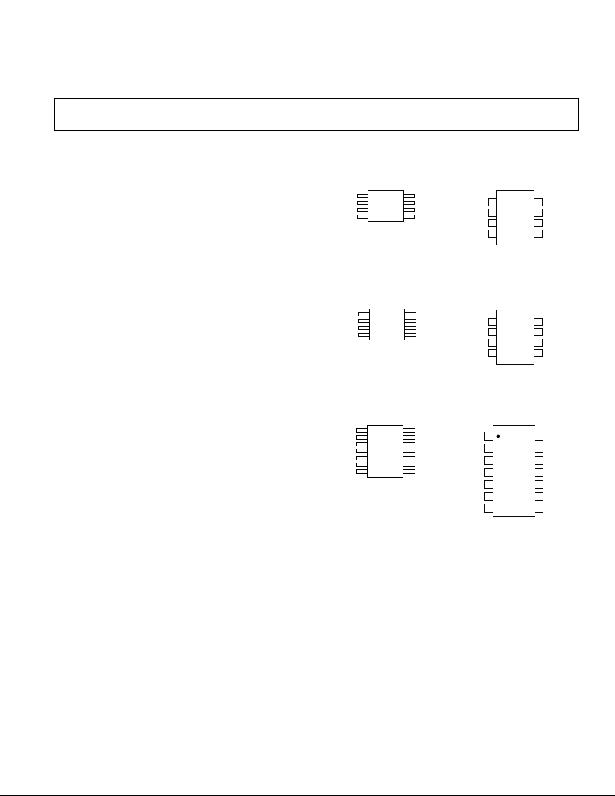
AD8551/AD8552/AD8554
8-Lead MSOP
(RM Suffix)
8-Lead TSSOP
(RU Suffix)
OUT A
2IN A
+IN A
OUT A
2IN A
1IN A
1IN B
2IN B
OUT B
1
AD8552
4
V2
14-Lead TSSOP
(RU Suffix)
1
V1
AD8554
78
Operational Amplifiers
PIN CONFIGURATIONS
8-Lead SOIC
(R Suffix)
8-Lead SOIC
(R Suffix)
8
V+
OUT B
2IN B
+IN B
5
14-Lead SOIC
(R Suffix)
OUT D
14
2IN D
1IN D
V2
1IN C
2IN C
OUT C
REV. 0
Information furnished by Analog Devices is believed to be accurate and
reliable. However, no responsibility is assumed by Analog Devices for its
use, nor for any infringements of patents or other rights of third parties
which may result from its use. No license is granted by implication or
otherwise under any patent or patent rights of Analog Devices.
One Technology Way, P.O. Box 9106, Norwood, MA 02062-9106, U.S.A.
Tel: 781/329-4700 World Wide Web Site: http://www.analog.com
Fax: 781/326-8703 © Analog Devices, Inc., 1999
Page 2

AD8551/AD8552/AD8554–SPECIFICATIONS
ELECTRICAL CHARACTERISTICS
(VS = +5 V, VCM = +2.5 V, VO = +2.5 V, TA = +25ⴗC unless otherwise noted)
Parameter Symbol Conditions Min Typ Max Units
INPUT CHARACTERISTICS␣
Offset Voltage V
Input Bias Current I
Input Offset Current I
B
OS
OS
–40°C ≤ T
–40°C ≤ T
–40°C ≤ T
≤ +125°C10µV
A
≤ +125°C 1.0 1.5 nA
A
≤ +125°C 150 200 pA
A
15 µV
10 50 pA
20 70 pA
Input Voltage Range 05V
Common-Mode Rejection Ratio CMRR V
Large Signal Voltage Gain
1
A
VO
= 0 V to +5 V 120 140 dB
CM
–40°C ≤ T
R
= 10 kΩ, V
L
–40°C ≤ T
≤ +125°C 115 130 dB
A
= +0.3 V to +4.7 V 125 145 dB
O
≤ +125°C 120 135 dB
A
Offset Voltage Drift ∆VOS/∆T –40°C ≤ TA ≤ +125°C 0.005 0.04 µV/°C
OUTPUT CHARACTERISTICS
Output Voltage High V
OH
R
= 100 kΩ to GND 4.99 4.998 V
L
–40°C to +125°C 4.99 4.997 V
= 10 kΩ to GND 4.95 4.98 V
R
L
–40°C to +125°C 4.95 4.975 V
R
Output Voltage Low V
OL
= 100 kΩ to V+ 1 10 mV
L
–40°C to +125°C210mV
= 10 kΩ to V+ 10 30 mV
R
L
–40°C to +125°C1530mV
Short Circuit Limit I
SC
±25 ±50 mA
–40°C to +125°C ±40 mA
Output Current I
O
±30 mA
–40°C to +125°C ±15 mA
POWER SUPPLY␣
Power Supply Rejection Ratio PSRR V
Supply Current/Amplifier I
SY
= +2.7 V to +5.5 V 120 130 dB
S
–40°C ≤ T
V
= 0 V 850 975 µA
O
≤ +125°C 115 130 dB
A
–40°C ≤ TA ≤ +125°C 1,000 1,075 µA
DYNAMIC PERFORMANCE␣
Slew Rate SR R
= 10 kΩ 0.4 V/µs
L
Overload Recovery Time 0.05 0.3 ms
Gain Bandwidth Product GBP 1.5 MHz
NOISE PERFORMANCE␣
Voltage Noise e
Voltage Noise Density e
Current Noise Density i
NOTE
1
Gain testing is highly dependent upon test bandwidth.
Specifications subject to change without notice.
p-p 0 Hz to 10 Hz 1.0 µV p-p
n
p-p 0 Hz to 1 Hz 0.32 µV p-p
e
n
n
n
f = 1 kHz 42 nV/√Hz
f = 10 Hz 2 fA/√Hz
–2– REV. 0
Page 3

AD8551/AD8552/AD8554
ELECTRICAL CHARACTERISTICS
(VS = +2.7 V, VCM = +1.35 V, VO = +1.35 V, TA = +25ⴗC unless otherwise noted)
Parameter Symbol Conditions Min Typ Max Units
INPUT CHARACTERISTICS␣
Offset Voltage V
Input Bias Current I
Input Offset Current I
B
OS
OS
–40°C ≤ T
–40°C ≤ T
–40°C ≤ T
≤ +125°C10µV
A
≤ +125°C 1.0 1.5 nA
A
≤ +125°C 150 200 pA
A
15 µV
10 50 pA
10 50 pA
Input Voltage Range 0 2.7 V
Common-Mode Rejection Ratio CMRR V
Large Signal Voltage Gain
1
A
VO
= 0 V to +2.7 V 115 130 dB
CM
–40°C ≤ T
R
= 10 kΩ, V
L
–40°C ≤ T
≤ +125°C 110 130 dB
A
= +0.3 V to +2.4 V 110 140 dB
O
≤ +125°C 105 130 dB
A
Offset Voltage Drift ∆VOS/∆T –40°C ≤ TA ≤ +125°C 0.005 0.04 µV/°C
OUTPUT CHARACTERISTICS
Output Voltage High V
OH
R
= 100 kΩ to GND 2.685 2.697 V
L
–40°C to +125°C 2.685 2.696 V
= 10 kΩ to GND 2.67 2.68 V
R
L
–40°C to +125°C 2.67 2.675 V
R
Output Voltage Low V
OL
= 100 kΩ to V+ 1 10 mV
L
–40°C to +125°C210mV
= 10 kΩ to V+ 10 20 mV
R
L
–40°C to +125°C1520mV
Short Circuit Limit I
SC
±10 ±15 mA
–40°C to +125°C ±10 mA
Output Current I
O
±10 mA
–40°C to +125°C ±5mA
POWER SUPPLY␣
Power Supply Rejection Ratio PSRR V
Supply Current/Amplifier I
SY
= +2.7 V to +5.5 V 120 130 dB
S
–40°C ≤ T
V
= 0 V 750 900 µA
O
≤ +125°C 115 130 dB
A
–40°C ≤ TA ≤ +125°C 950 1,000 µA
DYNAMIC PERFORMANCE␣
Slew Rate SR R
= 10 kΩ 0.5 V/µs
L
Overload Recovery Time 0.05 ms
Gain Bandwidth Product GBP 1 MHz
NOISE PERFORMANCE␣
Voltage Noise e
Voltage Noise Density e
Current Noise Density i
NOTE
1
Gain testing is highly dependent upon test bandwidth.
Specifications subject to change without notice.
p-p 0 Hz to 10 Hz 1.6 µV p-p
n
n
n
f = 1 kHz 75 nV/√Hz
f = 10 Hz 2 fA/√Hz
–3–REV. 0
Page 4
AD8551/AD8552/AD8554
WARNING!
ESD SENSITIVE DEVICE
ABSOLUTE MAXIMUM RATINGS
Supply Voltage . . . . . . . . . . . . . . . . . . . . . . . . . . . . . . . . . +6 V
Input Voltage . . . . . . . . . . . . . . . . . . . . . . GND to V
Differential Input Voltage
2
. . . . . . . . . . . . . . . . . . . . . . ±5.0 V
ESD(Human Body Model) . . . . . . . . . . . . . . . . . . . . . 2,000 V
Output Short-Circuit Duration to GND . . . . . . . . . Indefinite
Storage Temperature Range
RM, RU and R Packages . . . . . . . . . . . . . –65°C to +150°C
Operating Temperature Range
AD8551A/AD8552A/AD8554A . . . . . . . . –40°C to +125°C
Junction Temperature Range
RM, RU and R Packages . . . . . . . . . . . . . –65°C to +150°C
Lead Temperature Range (Soldering, 60 sec) . . . . . . . +300°C
NOTES
1
Stresses above those listed under Absolute Maximum Ratings may cause perma-
nent damage to the device. This is a stress rating only; functional operation of the
device at these or any other conditions above those listed in the operational sections
of this specification is not implied. Exposure to absolute maximum rating conditions for extended periods may affect device reliability.
2
Differential input voltage is limited to ±5.0 V or the supply voltage, whichever is less.
1
+ 0.3 V
S
ORDERING GUIDE
Package Type
1
JA
JC
Units
8-Lead MSOP (RM) 190 44 °C/W
8-Lead TSSOP (RU) 240 43 °C/W
8-Lead SOIC (R) 158 43 °C/W
14-Lead TSSOP (RU) 180 36 °C/W
14-Lead SOIC (R) 120 36 °C/W
NOTE
1
θJA is specified for worst case conditions, i.e., θ
for P-DIP packages, θ
SOIC and TSSOP packages.
is specified for device soldered in circuit board for
JA
is specified for device in socket
JA
Temperature Package Package
Model Range Description Option Brand
AD8551ARM
2
–40°C to +125°C 8-Lead MSOP RM-8 AHA
AD8551AR –40°C to +125°C 8-Lead SOIC SO-8
AD8552ARU
3
–40°C to +125°C 8-Lead TSSOP RU-8
AD8552AR –40°C to +125°C 8-Lead SOIC SO-8
AD8554ARU
3
–40°C to +125°C 14-Lead TSSOP RU-14
AD8554AR –40°C to +125°C 14-Lead SOIC SO-14
NOTES
1
Due to package size limitations, these characters represent the part number.
2
Available in reels only. 1,000 or 2,500 pieces per reel.
3
Available in reels only. 2,500 pieces per reel.
CAUTION
ESD (electrostatic discharge) sensitive device. Electrostatic charges as high as 4000 V readily
accumulate on the human body and test equipment and can discharge without detection. Although
the AD8551/AD8552/AD8554 features proprietary ESD protection circuitry, permanent damage
may occur on devices subjected to high energy electrostatic discharges. Therefore, proper ESD
precautions are recommended to avoid performance degradation or loss of functionality.
1
–4– REV. 0
Page 5
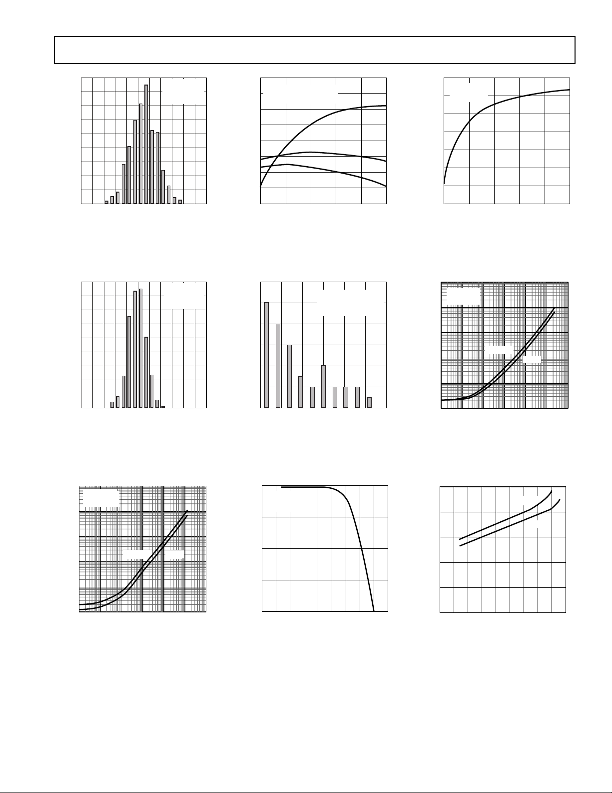
INPUT COMMON-MODE VOLTAGE – V
INPUT BIAS CURRENT – pA
1,500
22,000
01
5
234
1,000
500
0
21,000
21,500
2500
VSY = +5V
T
A
= +1258C
LOAD CURRENT – mA
10
0.1
0.001
OUTPUT VOLTAGE – mV
0.1
110
1
100
10k
100
1k
0.0001 0.01
SOURCE
SINK
VSY = +5V
T
A
= +258C
TEMPERATURE – 8C
SUPPLY CURRENT – mA
1.0
0.8
0
275 250
125
225
0
25 50 75 100
0.6
0.4
0.2
150
+5V
+2.7V
Typical Performance Characteristics–
AD8551/AD8552/AD8554
180
160
140
120
100
80
60
NUMBER OF AMPLIFIERS
40
20
0
21.5 20.5
22.5
OFFSET VOLTAGE – mV
0.5
VSY = +2.7V
= +1.35V
V
CM
= +258C
T
A
1.5
2.5
Figure 1. Input Offset Voltage
Distribution at +2.7 V
180
160
140
120
100
80
60
NUMBER OF AMPLIFIERS
40
20
0
22.5
21.5 20.5
OFFSET VOLTAGE – mV
VSY = +5V
= +2.5V
V
CM
T
= +258C
A
0.5 2.5
1.5
Figure 4. Input Offset Voltage
Distribution at +5 V
50
VSY = +5V
40
= 2408C, +258C, +858C
T
A
30
20
10
0
210
INPUT BIAS CURRENT – pA
220
230
01
INPUT COMMON-MODE VOLTAGE – V
234
+858C
+258C
2408C
Figure 2. Input Bias Current vs.
Common-Mode Voltage
12
VSY = +5V
= +2.5V
10
8
6
4
NUMBER OF AMPLIFIERS
2
0
01 6
INPUT OFFSET DRIFT – nV/8C
V
CM
T
= 2408C TO +1258C
A
234 5
Figure 5. Input Offset Voltage Drift
Distribution at +5 V
5
Figure 3. Input Bias Current vs.
Common-Mode Voltage
Figure 6. Output Voltage to Supply
Rail vs. Output Current at +5 V
10k
1k
100
10
OUTPUT VOLTAGE – mV
1
0.1
0.0001 0.01
Figure 7. Output Voltage to Supply
Rail vs. Output Current at +2.7 V
VSY = +2.7V
= +258C
T
A
SOURCE
0.001
0.1
LOAD CURRENT – mA
SINK
110
100
0
VCM = +2.5V
= +5V
V
SY
2250
2500
2750
INPUT BIAS CURRENT – pA
21000
275 250
225
0 25 50 75 100
TEMPERATURE – 8C
125
150
Figure 8. Bias Current vs. Temperature
–5–REV. 0
Figure 9. Supply Current vs.
Temperature
Page 6
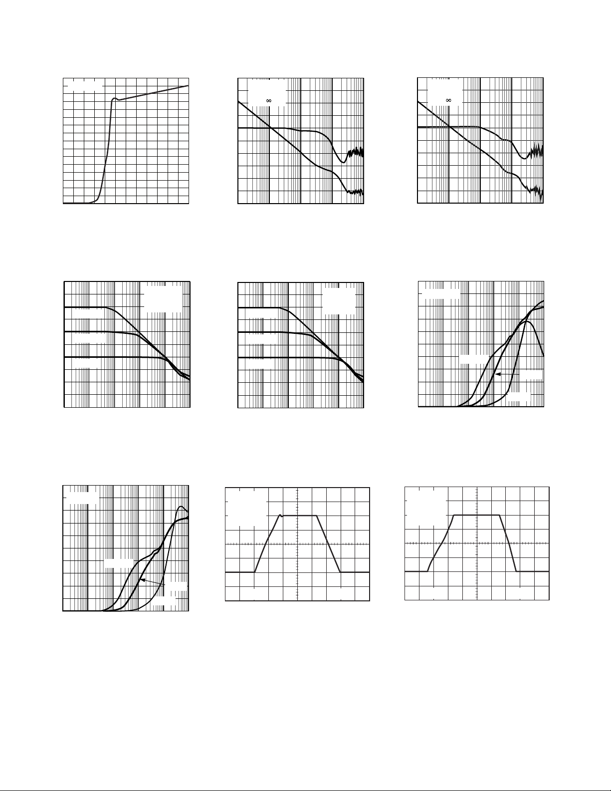
AD8551/AD8552/AD8554
g
FREQUENCY – Hz
OPEN-LOOP GAIN – dB
10k 100k 100M1M 10M
60
50
240
40
30
20
10
0
210
220
230
45
90
135
180
225
270
0
PHASE SHIFT – Degrees
VSY = +5V
C
L
= 0pF
R
L
=
FREQUENCY – Hz
OUTPUT IMPEDANCE – V
100 1k 10M10k 100k 1M
300
270
0
240
210
180
150
120
90
60
30
VSY = +2.7V
AV = 100
AV = 1
AV = 10
5ms
1V
VSY = +5V
C
L
= 300pF
R
L
= 2kV
A
V
= +1
800
TA = +258C
700
600
500
400
300
200
100
SUPPLY CURRENT PER AMPLIFIER – mA
0
0
16
2345
SUPPLY VOLTAGE – V
Figure 10. Supply Current vs.
Supply Voltage
60
50
40
AV = 2100
30
20
AV = 210
10
0
AV = +1
210
CLOSED-LOOP GAIN – dB
220
230
240
100 1k 10M10k 100k 1M
FREQUENCY – Hz
VSY = +2.7V
= 0pF
C
L
R
= 2kV
L
Figure 13. Closed Loop Gain vs.
Frequency at +2.7 V
60
VSY = +2.7V
50
40
30
20
10
210
OPEN-LOOP GAIN – dB
220
230
240
= 0pF
C
L
R
=
L
0
10k 100k 100M1M 10M
FREQUENCY – Hz
Figure 11. Open-Loop Gain and
Phase Shift vs. Frequency at +2.7 V
60
50
40
AV = 2100
30
20
AV = 210
10
0
AV = +1
210
CLOSED-LOOP GAIN – dB
220
230
240
100 1k 10M10k 100k 1M
FREQUENCY – Hz
VSY = +5V
= 0pF
C
L
R
= 2kV
L
Figure 14. Closed Loop Gain vs.
Frequency at +5 V
0
rees
45
90
135
180
225
PHASE SHIFT – De
270
Figure 12. Open-Loop Gain and
Phase Shift vs. Frequency at +5 V
Figure 15. Output Impedance vs.
Frequency at +2.7 V
300
VSY = +5V
270
240
210
180
150
120
90
OUTPUT IMPEDANCE – V
60
30
0
100 1k 10M10k 100k 1M
Figure 16. Output Impedance vs.
Frequency at +5 V
AV = 100
FREQUENCY – Hz
AV = 10
AV = 1
VSY = +2.7V
= 300pF
C
L
= 2kV
R
L
= +1
A
V
2ms
500mV
Figure 17. Large Signal Transient
Response at +2.7 V
–6– REV. 0
Figure 18. Large Signal Transient
Response at +5 V
Page 7

AD8551/AD8552/AD8554
CAPACITANCE – pF
SMALL SIGNAL OVERSHOOT – %
10 100 10k1k
50
45
0
40
35
30
25
20
15
10
5
+OS
2OS
VSY = 61.35V
R
L
= 2kV
T
A
= +258C
VSY = 62.5V
VIN = +200mV p-p
(RET TO GND)
C
L
= 0pF
R
L
= 10kV
A
V
= 2100
20ms
1V
V
IN
0V
0V
V
OUT
BOTTOM SCALE: 1V/DIV
TOP SCALE: 200mV/DIV
FREQUENCY – Hz
CMRR – dB
140
80
0
100 1k 10M10k 100k 1M
60
120
20
40
100
VSY = +5V
VSY = 61.35V
= 50pF
C
L
R
=
L
A
= +1
V
5ms
50mV
Figure 19. Small Signal Transient
Response at +2.7 V
45
VSY = 62.5V
40
R
= 2kV
L
T
= +258C
35
A
30
25
20
15
10
SMALL SIGNAL OVERSHOOT – %
5
0
10 100 10k1k
+OS
CAPACITANCE – pF
2OS
Figure 22. Small Signal Overshoot
vs. Load Capacitance at +5 V
VSY = 62.5V
= 50pF
C
L
R
=
L
= +1
A
V
5ms
50mV
Figure 20. Small Signal Transient
Response at +5 V
0V
V
IN
V
OUT
0V
20ms
BOTTOM SCALE: 1V/DIV
TOP SCALE: 200mV/DIV
VSY = 62.5V
V
= 2200mV p-p
IN
(RET TO GND)
= 0pF
C
L
R
= 10kV
L
= 2100
A
V
1V
Figure 23. Positive Overvoltage
Recovery
Figure 21. Small Signal Overshoot
vs. Load Capacitance at +2.7 V
Figure 24. Negative Overvoltage
Recovery
VS = 62.5V
R
A
V
200ms
Figure 25. No Phase Reversal
= 2kV
L
= 2100
V
= 60mV p-p
IN
140
VSY = +2.7V
120
100
80
60
CMRR – dB
40
1V
20
0
100 1k 10M10k 100k 1M
FREQUENCY – Hz
Figure 26. CMRR vs. Frequency
at +2.7 V
–7–REV. 0
Figure 27. CMRR vs. Frequency
at +5 V
Page 8

AD8551/AD8552/AD8554
FREQUENCY – Hz
OUTPUT SWING – V p-p
3.0
2.5
0
100 1k 1M10k 100k
2.0
1.5
0.5
1.0
VSY = 61.35V
R
L
= 2kV
A
V
= +1
THD+N < 1%
T
A
= +258C
1s
2mV
VSY = 62.5V
A
V
= 10,000
VSY = +5V
R
S
= 0V
0.5
FREQUENCY – kHz
1.0 1.5 2.0 2.50
26
39
52
65
78
91
13
e
n
– nV/ Hz
140
VSY = 61.35V
120
100
80
60
PSRR – dB
2PSRR
40
20
0
100 1k 10M10k 100k 1M
+PSRR
FREQUENCY – Hz
Figure 28. PSRR vs. Frequency
at
±
1.35 V
5.5
5.0
4.5
4.0
3.5
3.0
2.5
2.0
1.5
OUTPUT SWING – V p-p
1.0
0.5
0
100 1k 1M10k 100k
FREQUENCY – Hz
VSY = 62.5V
R
= 2kV
L
= +1
A
V
THD+N < 1%
T
= +258C
A
Figure 31. Maximum Output Swing
vs. Frequency at +5 V
140
VSY = 62.5V
120
100
80
60
PSRR – dB
2PSRR
40
20
0
100 1k 10M10k 100k 1M
+PSRR
FREQUENCY – Hz
Figure 29. PSRR vs. Frequency
at
±
2.5 V
VSY = 61.35V
= 10,000
A
V
0V
1s
2mV
Figure 32. 0.1 Hz to 10 Hz Noise
at +2.7 V
Figure 30. Maximum Output Swing
vs. Frequency at +2.7 V
Figure 33. 0.1 Hz to 10 Hz Noise at +5 V
182
156
130
104
– nV/ Hz
n
e
78
52
26
0.5
1.0 1.5 2.0 2.50
FREQUENCY – kHz
Figure 34. Voltage Noise Density at
+2.7 V from 0 Hz to 2.5 kHz
VSY = +2.7V
= 0V
R
S
112
96
80
64
– nV/ Hz
n
e
48
32
16
5
10 15 20 250
FREQUENCY – kHz
VSY = +2.7V
= 0V
R
S
Figure 35. Voltage Noise Density at
+2.7 V from 0 Hz to 25 kHz
–8– REV. 0
Figure 36. Voltage Noise Density at
+5 V from 0 Hz to 2.5 kHz
Page 9

AD8551/AD8552/AD8554
TEMPERATURE – 8C
POWER SUPPLY REJECTION – dB
150
145
125
275 250
125
225
0
25 50 75 100
140
135
130
150
VSY = +2.7V TO +5.5V
100
TEMPERATURE – 8C
OUTPUT VOLTAGE SWING – mV
250
200
0
275 250
125
225
0
25 50 75 100
150
150
VSY = +5.0V
25
50
75
125
175
225
RL = 1kV
RL = 10kV
RL = 100kV
112
96
80
64
– nV/ Hz
n
e
48
32
16
5101520250
FREQUENCY – kHz
VSY = ±5V
= 0V
R
S
Figure 37. Voltage Noise Density
at +5 V from 0 Hz to 25 kHz
50
VSY = +2.7V
40
30
20
0
210
220
230
SHORT-CIRCUIT CURRENT – mA
240
250
275 250
225
0
25 50 75 10010150
TEMPERATURE – 8C
I
SC2
I
SC+
125
Figure 40. Output Short-Circuit
Current vs. Temperature
168
144
120
96
– nV/ Hz
n
72
e
48
24
5100
FREQUENCY – Hz
VSY = +5V
= 0V
R
S
Figure 38. Voltage Noise Density
at +5 V from 0 Hz to 10 Hz
100
VSY = +5.0V
80
60
40
0
220
240
260
SHORT-CIRCUIT CURRENT – mA
280
2100
275 250
225
0
25 50 75 10020150
TEMPERATURE – 8C
I
SC2
I
SC+
125
Figure 41. Output Short-Circuit
Current vs. Temperature
Figure 39. Power-Supply Rejection
vs. Temperature
Figure 42. Output Voltage to
Supply Rail vs. Temperature
250
VSY = +5.0V
225
200
175
150
125
100
75
50
OUTPUT VOLTAGE SWING – mV
25
0
275 250
Figure 43. Output Voltage to Supply
Rail vs. Temperature
RL = 10kV
225
0
TEMPERATURE – 8C
RL = 1kV
RL = 100kV
25 50 75 100
125
150
–9–REV. 0
Page 10

AD8551/AD8552/AD8554
FUNCTIONAL DESCRIPTION
The AD855x family of amplifiers are high precision rail-to-rail
operational amplifiers that can be run from a single supply volt-
age. Their typical offset voltage of less than 1 µV allows these
amplifiers to be easily configured for high gains without risk of
excessive output voltage errors. The extremely small tempera-
ture drift of 5 nV/°C ensures a minimum of offset voltage error
over its entire temperature range of –40°C to +125°C, making
the AD855x amplifiers ideal for a variety of sensitive measurement applications in harsh operating environments such as
under-hood and braking/suspension systems in automobiles.
The AD855x family are CMOS amplifiers and achieve their
high degree of precision through autozero stabilization. This
autocorrection topology allows the AD855x to maintain its low
offset voltage over a wide temperature range and over its operating lifetime.
Amplifier Architecture
Each AD855x op amp consists of two amplifiers, a main amplifier
and a secondary amplifier, used to correct the offset voltage of the
main amplifier. Both consist of a rail-to-rail input stage, allowing
the input common-mode voltage range to reach both supply rails.
The input stage consists of an NMOS differential pair operating
concurrently with a parallel PMOS differential pair. The outputs
from the differential input stages are combined in another gain
stage whose output is used to drive a rail-to-rail output stage.
The wide voltage swing of the amplifier is achieved by using two
output transistors in a common-source configuration. The output
voltage range is limited by the drain to source resistance of these
transistors. As the amplifier is required to source or sink more
output current, the r
of these transistors increases, raising the
DS
voltage drop across these transistors. Simply put, the output voltage will not swing as close to the rail under heavy output current
conditions as it will with light output current. This is a characteristic of all rail-to-rail output amplifiers. Figures 6 and 7 show how
close the output voltage can get to the rails with a given output
current. The output of the AD855x is short circuit protected to
approximately 50 mA of current.
The AD855x amplifiers have exceptional gain, yielding greater
than 120 dB of open-loop gain with a load of 2 kΩ. Because the
output transistors are configured in a common-source configuration, the gain of the output stage, and thus the open-loop gain
of the amplifier, is dependent on the load resistance. Open-loop
gain will decrease with smaller load resistances. This is another
characteristic of rail-to-rail output amplifiers.
Basic Autozero Amplifier Theory
Autocorrection amplifiers are not a new technology. Various IC
implementations have been available for over 15 years and some
improvements have been made over time. The AD855x design
offers a number of significant performance improvements over
older versions while attaining a very substantial reduction in device cost. This section offers a simplified explanation of how the
AD855x is able to offer extremely low offset voltages and high
open-loop gains.
As noted in the previous section on amplifier architecture, each
AD855x op amp contains two internal amplifiers. One is used as
the primary amplifier, the other as an autocorrection, or nulling,
amplifier. Each amplifier has an associated input offset voltage,
which can be modeled as a dc voltage source in series with the
noninverting input. In Figures 44 and 45 these are labeled as
, where x denotes the amplifier associated with the offset; A
V
OSX
for the nulling amplifier, B for the primary amplifier. The openloop gain for the +IN and –IN inputs of each amplifier is given
. Both amplifiers also have a third voltage input with an
as A
X
associated open-loop gain of B
.
X
There are two modes of operation determined by the action of
two sets of switches in the amplifier: An autozero phase and an
amplification phase.
Autozero Phase
In this phase, all φA switches are closed and all φB switches are
opened. Here, the nulling amplifier is taken out of the gain loop
by shorting its two inputs together. Of course, there is a degree of
offset voltage, shown as V
, inherent in the nulling amplifier
OSA
which maintains a potential difference between the +IN and –IN
inputs. The nulling amplifier feedback loop is closed through φA
and V
appears at the output of the nulling amp and on CM1,
OSA
2
an internal capacitor in the AD855x. Mathematically, we can express this in the time domain as:
Vt AV tBVt
=
[]
OA A OSA A OA
−
[]
(1)
[]
which can be expressed as,
Vt
[]
OA
AV t
=
A OSA
+1
B
[]
(2)
A
This shows us that the offset voltage of the nulling amplifier
times a gain factor appears at the output of the nulling amplifier
and thus on the C
V
IN+
V
IN2
capacitor.
M1
FB
FA
A
V
OA
V
OSA
+
A
FB
A
2B
A
FA
V
NA
V
B
OUT
B
B
C
M2
V
NB
C
M1
Figure 44. Autozero Phase of the AD855x
Amplification Phase
When the φB switches close and the φA switches open for the
amplification phase, this offset voltage remains on C
M1
and
essentially corrects any error from the nulling amplifier. The
voltage across C
as the potential difference between the two inputs to the
V
IN
primary amplifier, or V
is designated as VNA. Let us also designate
M1
IN
= (V
IN+
– V
). Now the output of the
IN–
nulling amplifier can be expressed as:
=
[]
OA A IN OSA A NA
[]−[]
()
−
(3)
[]
Vt AVtV t BVt
–10– REV. 0
Page 11

AD8551/AD8552/AD8554
V
IN+
V
IN2
FB
FA
V
OSA
V
+
OA
A
A
2B
A
FB
A
FA
V
NA
V
B
OUT
B
B
C
M2
V
NB
C
M1
Figure 45. Output Phase of the Amplifier
Because φA is now open and there is no place for C
charge, the voltage V
voltage at the output of the nulling amp V
at the present time t is equal to the
NA
at the time when
OA
to dis-
M1
φA was closed. If we call the period of the autocorrection
switching frequency T
phases every 0.5␣ ⫻␣ T
, then the amplifier switches between
S
. Therefore, in the amplification phase:
S
VtV t T
[]
NA NA S
=−
1
(4)
2
And substituting Equation 4 and Equation 2 into Equation 3 yields:
1
−
2
(5)
Vt AVtAV t
=
[]
OA A IN A OSA
+
[]
ABV t T
A A OSA S
−
[]
1
+
B
A
For the sake of simplification, let us assume that the autocorrection
frequency is much faster than any potential change in V
. This is a good assumption since changes in offset voltage are
V
OSB
OSA
or
a function of temperature variation or long-term wear time, both of
which are much slower than the auto-zero clock frequency of the
AD855x. This effectively makes V
time invariant and we can re-
OS
arrange Equation 5 and rewrite it as:
Vt AVt
=
[]
OA A IN
+
1
()
A A OSA A A OSA
+
[]
−
B
+
1
A
(6)
ABV ABV
or,
Vt AVt
[]
OA A IN
=
[]
+
V
OSA
(7)
+
1
B
A
We can already get a feel for the autozeroing in action. Note the
term is reduced by a 1 + BA factor. This shows how the
V
OS
nulling amplifier has greatly reduced its own offset voltage error
even before correcting the primary amplifier. Now the primary
amplifier output voltage is the voltage at the output of the
AD855x amplifier. It is equal to:
VtAVtV BV
=
[]
OUT B IN OSB B NB
+
[]
()
+
(8)
In the amplification phase, VOA = VNB, so this can be rewritten as:
VtAVtAV BAVt
=
[]
OUT B IN B OSB B A IN
++
[]
+
[]
1
V
OSA
+
(9)
B
A
Combining terms,
ABV
VtVtAAB
[]=[]
OUT IN B A B
+
()
+
A B OSA
+
1
B
A
+
AV
B OSB
(10)
The AD855x architecture is optimized in such a way that
A
␣=␣AB and BA␣=␣BB and BA␣ >>␣ 1. Also, the gain product of
A
is much greater than AB. These allow Equation 10 to be
A
ABB
simplified to:
VtVtABAV V
[]≈[]
OUT IN A A A OSA OSB
++
()
(11)
Most obvious is the gain product of both the primary and nulling
amplifiers. This A
high open-loop gain. To understand how V
term is what gives the AD855x its extremely
ABA
OSA
and V
relate to
OSB
the overall effective input offset voltage of the complete amplifier,
we should set up the generic amplifier equation of:
VkVV
Where k is the open-loop gain of an amplifier and V
=× +
OUT IN OS EFF
()
(12)
,
OS, EFF
is its
effective offset voltage. Putting Equation 12 into the form of
Equation 11 gives us:
VtVtABV AB
[]≈[]
OUT IN A A OS EFF A A
+
,
(13)
And from here, it is easy to see that:
VV
+
V
OS EFF
,
OSA OSB
≈
B
(14)
A
Thus, the offset voltages of both the primary and nulling amplifiers are reduced by the gain factor B
. This takes a typical input
A
offset voltage from several millivolts down to an effective input
offset voltage of submicrovolts. This autocorrection scheme is
what makes the AD855x family of amplifiers among the most
precise amplifiers in the world.
High Gain, CMRR, PSRR
Common-mode and power supply rejection are indications of
the amount of offset voltage an amplifier has as a result of a
change in its input common-mode or power supply voltages. As
shown in the previous section, the autocorrection architecture of
the AD855x allows it to quite effectively minimize offset voltages. The technique also corrects for offset errors caused by
common-mode voltage swings and power supply variations.
This results in superb CMRR and PSRR figures in excess of
130 dB. Because the autocorrection occurs continuously, these
figures can be maintained across the device’s entire temperature
range, from –40°C to +125°C.
Maximizing Performance Through Proper Layout
To achieve the maximum performance of the extremely high
input impedance and low offset voltage of the AD855x, care
should be taken in the circuit board layout. The PC board surface must remain clean and free of moisture to avoid leakage
currents between adjacent traces. Surface coating of the circuit
board will reduce surface moisture and provide a humidity
barrier, reducing parasitic resistance on the board. The use of
guard rings around the amplifier inputs will further reduce leakage currents. Figure 46 shows how the guard ring should be
configured and Figure 47 shows the top view of how a surface
mount layout can be arranged. The guard ring does not need to
–11–REV. 0
Page 12

AD8551/AD8552/AD8554
SURFACE MOUNT
COMPONENT
COMPONENT
LEAD
SOLDER
PC BOARD
COPPER
TRACE
V
SC2
2
+
+
2
V
TS2
T
A2
T
A1
V
SC1
2
+
+
2
V
TS1
IF TA1 fi TA2, THEN
V
TS1
+ V
SC1
fi V
TS2
+ V
SC2
be a specific width, but it should form a continuous loop around
both inputs. By setting the guard ring voltage equal to the voltage at the noninverting input, parasitic capacitance is minimized
as well. For further reduction of leakage currents, components
can be mounted to the PC board using Teflon standoff insulators.
V
OUT
V
IN
V
IN
AD8552
V
IN
AD8552
V
OUT
AD8552
Figure 46. Guard Ring Layout and Connections to Reduce
PC Board Leakage Currents
V+
R
R
2
1
V
IN2
GUARD
RING
V
REF
V
IN1
GUARD
RING
R
V
REF
R
1
2
AD8552
V2
Figure 47. Top View of AD8552 SOIC Layout with
Guard Rings
Other potential sources of offset error are thermoelectric voltages
on the circuit board. This voltage, also called Seebeck voltage,
occurs at the junction of two dissimilar metals and is proportional
to the temperature of the junction. The most common metallic
junctions on a circuit board are solder-to-board trace and solderto-component lead. Figure 48 shows a cross-section diagram view
of the thermal voltage error sources. If the temperature of the PC
board at one end of the component (T
temperature at the other end (T
), the Seebeck voltages will not
A2
) is different from the
A1
be equal, resulting in a thermal voltage error.
This thermocouple error can be reduced by using dummy components to match the thermoelectric error source. Placing the
dummy component as close as possible to its partner will ensure
both Seebeck voltages are equal, thus canceling the thermocouple error. Maintaining a constant ambient temperature on
the circuit board will further reduce this error. The use of a
ground plane will help distribute heat throughout the board and
will also reduce EMI noise pickup.
V
OUT
Figure 48. Mismatch in Seebeck Voltages Causes a
Thermoelectric Voltage Error
R
F
R
1
V
V
IN
RS = R
1
NOTE: RS SHOULD BE PLACED IN CLOSE PROXIMITY AND
ALIGNMENT TO R
TO BALANCE SEEBECK VOLTAGES
1
AD855x
AV = 1 + (RF/R1)
OUT
Figure 49. Using Dummy Components to Cancel
Thermoelectric Voltage Errors
1/f Noise Characteristics
Another advantage of autozero amplifiers is their ability to cancel
flicker noise. Flicker noise, also known as 1/f noise, is noise inherent in the physics of semiconductor devices and increases 3 dB
for every octave decrease in frequency. The 1/f corner frequency
of an amplifier is the frequency at which the flicker noise is equal
to the broadband noise of the amplifier. At lower frequencies,
flicker noise dominates, causing higher degrees of error for subHertz frequencies or dc precision applications.
Because the AD855x amplifiers are self-correcting op amps,
they do not have increasing flicker noise at lower frequencies.
In essence, low frequency noise is treated as a slowly varying
offset error and is greatly reduced as a result of autocorrection.
The correction becomes more effective as the noise frequency
approaches dc, offsetting the tendency of the noise to increase
exponentially as frequency decreases. This allows the AD855x
to have lower noise near dc than standard low-noise amplifiers
that are susceptible to 1/f noise.
Intermodulation Distortion
The AD855x can be used as a conventional op amp for gain/
bandwidth combinations up to 1.5 MHz. The autozero correction frequency of the device is fixed at 4 kHz. Although a trace
amount of this frequency will feed through to the output, the
amplifier can be used at much higher frequencies. Figure 50
shows the spectral output of the AD8552 with the amplifier
configured for unity gain and the input grounded.
The 4 kHz autozero clock frequency appears at the output with
less than 2 µV of amplitude. Harmonics are also present, but at
reduced levels from the fundamental autozero clock frequency.
The amplitude of the clock frequency feedthrough is proportional
to the closed-loop gain of the amplifier. Like other autocorrection
amplifiers, at higher gains there will be more clock frequency
feedthrough. Figure 51 shows the spectral output with the amplifier configured for a gain of 60 dB.
–12– REV. 0
Page 13

AD8551/AD8552/AD8554
V
IN
= 1mV rms
@ 200Hz
100V
100kV
3.3nF
0
220
240
260
280
OUTPUT SIGNAL
2100
2120
2140
0
23456789
FREQUENCY – kHz
VSY = +5V
= 0dB
A
V
101
Figure 50. Spectral Analysis of AD855x Output in Unity
Gain Configuration
0
220
240
260
280
OUTPUT SIGNAL
2100
VSY = +5V
= +60dB
A
V
0
OUTPUT SIGNAL
1Vrms @ 200Hz
220
240
260
OUTPUT SIGNAL
280
2100
2120
0
IMD < 100mVrms
23456789
FREQUENCY – kHz
VSY = +5V
= +60dB
A
V
101
Figure 52. Spectral Analysis of AD855x in High Gain with
a 1 mV Input Signal
For most low frequency applications, the small amount of autozero clock frequency feedthrough will not affect the precision of the
measurement system. Should it be desired, the clock frequency
feedthrough can be reduced through the use of a feedback capacitor around the amplifier. However, this will reduce the bandwidth
of the amplifier. Figures 53a and 53b show a configuration for
reducing the clock feedthrough and the corresponding spectral
analysis at the output. The –3 dB bandwidth of this configuration
is 480 Hz.
2120
2140
0
23456789
FREQUENCY – kHz
101
Figure 51. Spectral Analysis of AD855x Output with
+60 dB Gain
When an input signal is applied, the output will contain some
degree of Intermodulation Distortion (IMD). This is another
characteristic feature of all autocorrection amplifiers. IMD will
show up as sum and difference frequencies between the input signal and the 4 kHz clock frequency (and its harmonics) and is at a
level similar to or less than the clock feedthrough at the output.
The IMD is also proportional to the closed loop gain of the amplifier. Figure 52 shows the spectral output of an AD8552 configured
as a high gain stage (+60 dB) with a 1 mV input signal applied.
The relative levels of all IMD products and harmonic distortion
add up to produce an output error of –60 dB relative to the input
signal. At unity gain, these would add up to only –120 dB relative
to the input signal.
Figure 53a. Reducing Autocorrection Clock Noise with a
Feedback Capacitor
0
220
240
260
OUTPUT SIGNAL
280
2100
2120
0
23456789
FREQUENCY – kHz
VSY = +5V
= +60dB
A
V
101
Figure 53b. Spectral Analysis Using a Feedback Capacitor
–13–REV. 0
Page 14

AD8551/AD8552/AD8554
+5V
R
X
60V
V
OUT
V
IN
200mV p-p
AD855x
C
L
4.7nF
C
X
0.47mF
Broadband and External Resistor Noise Considerations
The total broadband noise output from any amplifier is primarily
a function of three types of noise: Input voltage noise from the
amplifier, input current noise from the amplifier and Johnson
noise from the external resistors used around the amplifier. Input
voltage noise, or e
, is strictly a function of the amplifier used.
n
The Johnson noise from a resistor is a function of the resistance
and the temperature. Input current noise, or i
, creates an equiva-
n
lent voltage noise proportional to the resistors used around the
amplifier. These noise sources are not correlated with each other
and their combined noise sums in a root-squared-sum fashion.
The full equation is given as:
1
2
2
e e kTr i r
n TOTAL n S n S,
=+ +
4
2
()
(15)
Where, en= The input voltage noise of the amplifier,
= The input current noise of the amplifier,
i
n
= Source resistance connected to the noninverting
r
S
terminal,
k = Boltzmann’s constant (1.38 ⫻ 10
-23
J/K)
T = Ambient temperature in Kelvin (K = 273.15 + °C)
The input voltage noise density, e
and the input noise, i
is 2 fA/√Hz. The e
n,
of the AD855x is 42 nV/√Hz,
n
n, TOTAL
will be domi-
nated by input voltage noise provided the source resistance is less
than 106 kΩ. With source resistance greater than 106 kΩ, the
overall noise of the system will be dominated by the Johnson
noise of the resistor itself.
Because the input current noise of the AD855x is very small, i
does not become a dominant term unless r
is greater than 4 GΩ,
S
n
which is an impractical value of source resistance.
The total noise, e
, is expressed in volts per square-root
n, TOTAL
Hertz, and the equivalent rms noise over a certain bandwidth
can be found as:
ee BW
=×
n n TOTAL
,
(16)
Where BW is the bandwidth of interest in Hertz.
For a complete treatise on circuit noise analysis, please refer to the
1995 Linear Design Seminar book available from Analog Devices.
Output Overdrive Recovery
The AD855x amplifiers have an excellent overdrive recovery of
only 200 µs from either supply rail. This characteristic is particu-
larly difficult for autocorrection amplifiers, as the nulling amplifier
requires a nontrivial amount of time to error correct the main amplifier back to a valid output. Figure 23 and Figure 24 show the
positive and negative overdrive recovery time for the AD855x.
The output overdrive recovery for an autocorrection amplifier is
defined as the time it takes for the output to correct to its final
voltage from an overload state. It is measured by placing the
amplifier in a high gain configuration with an input signal that
forces the output voltage to the supply rail. The input voltage is
then stepped down to the linear region of the amplifier, usually
to half-way between the supplies. The time from the input signal
step-down to the output settling to within 100 µV of its final
value is the overdrive recovery time. Most competitors’ autocorrection amplifiers require a number of autozero clock cycles
to recover from output overdrive and some can take several
milliseconds for the output to settle properly.
Input Overvoltage Protection
Although the AD855x is a rail-to-rail input amplifier, care should
be taken to ensure that the potential difference between the inputs does not exceed +5 V. Under normal operating conditions,
the amplifier will correct its output to ensure the two inputs are at
the same voltage. However, if the device is configured as a comparator, or is under some unusual operating condition, the input
voltages may be forced to different potentials. This could cause
excessive current to flow through internal diodes in the AD855x
used to protect the input stage against overvoltage.
If either input exceeds either supply rail by more than 0.3 V, large
amounts of current will begin to flow through the ESD protection
diodes in the amplifier. These diodes are connected between the
inputs and each supply rail to protect the input transistors against
an electrostatic discharge event and are normally reverse-biased.
However, if the input voltage exceeds the supply voltage, these
ESD diodes will become forward-biased. Without current limiting, excessive amounts of current could flow through these diodes
causing permanent damage to the device. If inputs are subject to
overvoltage, appropriate series resistors should be inserted to
limit the diode current to less than 2 mA maximum.
Output Phase Reversal
Output phase reversal occurs in some amplifiers when the input
common-mode voltage range is exceeded. As common-mode voltage is moved outside of the common-mode range, the outputs of
these amplifiers will suddenly jump in the opposite direction to the
supply rail. This is the result of the differential input pair shutting
down, causing a radical shifting of internal voltages which results in
the erratic output behavior.
The AD855x amplifier has been carefully designed to prevent
any output phase reversal, provided both inputs are maintained
within the supply voltages. If one or both inputs could exceed
either supply voltage, a resistor should be placed in series with
the input to limit the current to less than 2 mA. This will ensure
the output will not reverse its phase.
Capacitive Load Drive
The AD855x has excellent capacitive load driving capabilities
and can safely drive up to 10 nF from a single +5 V supply.
Although the device is stable, capacitive loading will limit the
bandwidth of the amplifier. Capacitive loads will also increase
the amount of overshoot and ringing at the output. An R-C
snubber network, Figure 54, can be used to compensate the
amplifier against capacitive load ringing and overshoot.
Figure 54. Snubber Network Configuration for Driving
Capacitive Loads
Although the snubber will not recover the loss of amplifier bandwidth from the load capacitance, it will allow the amplifier to drive
larger values of capacitance while maintaining a minimum of
overshoot and ringing. Figure 55 shows the output of an AD855x
driving a 1 nF capacitor with and without a snubber network.
–14– REV. 0
Page 15

WITH
V
SY
= 0V TO +5V
100kV
AD855x
100kV
V
OUT
V
OUT
350V
LOAD
CELL
AD8552-A
R
1
17.4kV
R
2
100V
0V TO +4.0V
NOTE: USE 0.1% TOLERANCE RESISTORS.
20kV
A1
A2
AD8552-B
REF192
12.0kV
1kV
+5V
+2.5V
6
4
3
2
+4.0V
40mV
FULL-SCALE
Q1
2N2222
OR
EQUIVALENT
R
3
17.4kV
R
4
100V
SNUBBER
AD8551/AD8552/AD8554
10ms
WITHOUT
SNUBBER
VSY = +5V
C
= 4.7nF
LOAD
100mV
Figure 55. Overshoot and Ringing are Substantially
Reduced Using a Snubber Network
The optimum value for the resistor and capacitor is a function of
the load capacitance and is best determined empirically since
actual C
will include stray capacitances and may differ sub-
LOAD
stantially from the nominal capacitive load. Table I shows some
snubber network values that can be used as starting points.
Table I. Snubber Network Values for Driving Capacitive Loads
C
LOAD
R
X
C
X
1 nF 200 Ω 1 nF
4.7 nF 60 Ω 0.47 µF
10 nF 20 Ω 10 µF
Power-Up Behavior
On power-up, the AD855x will settle to a valid output within 5 µs.
Figure 56a shows an oscilloscope photo of the output of the amplifier along with the power supply voltage, and Figure 56b shows
the test circuit. With the amplifier configured for unity gain, the
device takes approximately 5 µs to settle to its final output voltage.
This turn-on response time is much faster than most other autocorrection amplifiers, which can take hundreds of microseconds or
longer for their output to settle.
Figure 56b. AD855x Test Circuit for Turn-On Time
APPLICATIONS
A +5 V Precision Strain-Gage Circuit
The extremely low offset voltage of the AD8552 makes it an
ideal amplifier for any application requiring accuracy with high
gains, such as a weigh scale or strain-gage. Figure 57 shows a
configuration for a single supply, precision strain-gage measurement system.
A REF192 provides a +2.5 V precision reference voltage for A2.
The A2 amplifier boosts this voltage to provide a +4.0 V reference
for the top of the strain-gage resistor bridge. Q1 provides the cur-
rent drive for the 350 Ω bridge network. A1 is used to amplify the
output of the bridge with the full-scale output voltage equal to:
2
×+
RR
()
12
R
B
(17)
Where RB is the resistance of the load cell. Using the values given
in Figure 57, the output voltage will linearly vary from 0 V with
no strain to +4.0 V under full strain.
V
OUT
Figure 56a. AD855x Output Behavior on Power-Up
0V
V+
0V
5ms
BOTTOM TRACE = 2V/DIV
TOP TRACE = 1V/DIV
Figure 57. A +5 V Precision Strain-Gage Amplifier
+3 V Instrumentation Amplifier
The high common-mode rejection, high open-loop gain, and
operation down to +3 V of supply voltage makes the AD855x
1V
an excellent choice of op amp for discrete single supply instrumentation amplifiers. The common-mode rejection ratio of
the AD855x is greater than 120 dB, but the CMRR of the system is also a function of the external resistor tolerances. The
gain of the difference amplifier shown in Figure 58 is given as:
VV
OUT
112
=
RRRR
R
4
+
+
3412
R
2
−
V
(18)
R
1
–15–REV. 0
Page 16

AD8551/AD8552/AD8554
AD8551
3
2
8
4
0V TO 5.00V
(08C TO 5008C)
+5V
0.1mF
+
10mF
R
9
124kV
R
8
453V
R
5
40.2kV
R
1
10.7kV
R
2
2.74kV
REF02EZ
0.1mF
+12V
2 6
4
++
––
D1
1N4148
R
3
53.6V
R
4
5.62kV
+5.000V
K-TYPE
THERMOCOUPLE
40.7mV/8C
R
6
200V
1
R
2
R
V2
V1
Figure 58. Using the AD855x as a Difference Amplifier
In an ideal difference amplifier, the ratio of the resistors are set
exactly equal to:
Which sets the output voltage of the system to:
1
V
OUT
R
3
R
4
R
R
4
=
R
3
A
V
2
, THEN V
R
1
RRR
2
==
1
IF
AD855x
R
2
3 (V1 2 V2)
=
OUT
R
1
4
(19)
R
3
A High Accuracy Thermocouple Amplifier
Figure 60 shows a K-type thermocouple amplifier configuration
with cold-junction compensation. Even from a +5 V supply, the
AD8551 can provide enough accuracy to achieve a resolution
of better than 0.02°C from 0°C to 500°C. D1 is used as a
temperature measuring device to correct the cold-junction error
from the thermocouple and should be placed as close as possible
to the two terminating junctions. With the thermocouple measuring tip immersed in a zero-degree ice bath, R
should be
6
adjusted until the output is at 0 V.
Using the values shown in Figure 60, the output voltage will
track temperature at 10 mV/°C. For a wider range of tempera-
ture measurement, R
can be decreased to 62 kΩ. This will
9
create a 5 mV/°C change at the output, allowing measurements
of up to 1000°C.
Due to finite component tolerance the ratio between the four
resistors will not be exactly equal, and any mismatch results in a
reduction of common-mode rejection from the system. Referring
to Figure 58, the exact common-mode rejection ratio can be expressed as:
In the 3 op amp instrumentation amplifier configuration shown
in Figure 59, the output difference amplifier is set to unity gain
with all four resistors equal in value. If the tolerance of the resis-
tors used in the circuit is given as δ, the worst-case CMRR of
the instrumentation amplifier will be:
Figure 59. A Discrete Instrumentation Amplifier
Configuration
Thus, using 1% tolerance resistors would result in a worst-case
system CMRR of 0.02, or 34 dB. Therefore either high precision
resistors or an additional trimming resistor, as shown in Figure
59, should be used to achieve high common-mode rejection. The
value of this trimming resistor should be equal to the value of R
multiplied by its tolerance. For example, using 10 kΩ resistors
with 1% tolerance would require a series trimming resistor equal to
100 Ω.
CMRR
V2
R
G
V1
V
= 1 +
OUT
VAVV
=−
OUT V
RR RR RR
14 24 23
=
CMRR
12 (20)
()
2
++
22
RR R R
−
14 2 3
=
MIN
AD8554-A
R
R
R
TRIM
R
R
AD8554-B
2R
R
G
(V1 2 V2)
(21)
1
(22)
2δ
R
AD8554-C
R
Figure 60. A Precision K-Type Thermocouple Amplifier
with Cold-Junction Compensation
Precision Current Meter
Because of its low input bias current and superb offset voltage at
single supply voltages, the AD855x is an excellent amplifier for
precision current monitoring. Its rail-to-rail input allows the
amplifier to be used as either a high-side or low-side current
monitor. Using both amplifiers in the AD8552 provides a simple
method to monitor both current supply and return paths for
V
OUT
load or fault detection.
Figure 61 shows a high-side current monitor configuration. Here,
the input common-mode voltage of the amplifier will be at or near
the positive supply voltage. The amplifier’s rail-to-rail input provides
a precise measurement even with the input common-mode voltage at
the supply voltage. The CMOS input structure does not draw any
input bias current, ensuring a minimum of measurement error.
The 0.1 Ω resistor creates a voltage drop to the noninverting
input of the AD855x. The amplifier’s output is corrected until
this voltage appears at the inverting input. This creates a current
through R
, which in turn flows through R2. The Monitor Output
1
is given by:
Monitor Output R
=×
R
2
SENSE
R
1
×
I
L
(23)
Using the components shown in Figure 61, the Monitor Output
transfer function is 2.5␣ V/A.
–16– REV. 0
Page 17

AD8551/AD8552/AD8554
Figure 62 shows the low-side monitor equivalent. In this circuit,
the input common-mode voltage to the AD8552 will be at or near
ground. Again, a 0.1 Ω resistor provides a voltage drop propor-
tional to the return current. The output voltage is given as:
R
VV
=+− × ×
OUT SENSE L
2
RI
R
1
(24)
For the component values shown in Figure 62, the output transfer function decreases from V+ at –2.5 V/A.
R
+3V
MONITOR
OUTPUT
100V
Si9433
M1
SENSE
0.1V
R
1
S
G
D
R
2
2.49kV
3
AD8552
2
+3V
1/2
I
L
V+
0.1mF
8
1
4
Figure 61. A High-Side Load Current Monitor
V+
R
2
Q1
2.49kV
R
1
100V
0.1V
R
SENSE
V+
1/2 AD8552
RETURN TO
GROUND
V
OUT
Figure 62. A Low-Side Load Current Monitor
Precision Voltage Comparator
The AD855x can be operated open-loop and used as a precision
comparator. The AD855x has less than 50 µV of offset voltage
when run in this configuration. The slight increase of offset
voltage stems from the fact that the autocorrection architecture
operates with lowest offset in a closed loop configuration, that
is, one with negative feedback. With 50 mV of overdrive, the de-
vice has a propagation delay of 15 µs on the rising edge and
8 µs on the falling edge.
Care should be taken to ensure the maximum differential voltage of the device is not exceeded. For more information, please
refer to the section on Input Overvoltage Protection.
SPICE Model
The SPICE macro-model for the AD855x amplifier is given in
Listing 1. This model simulates the typical specifications for the
AD855x, and it can be downloaded from the Analog Devices
website at http://www.analog.com. The schematic of the
macro-model is shown in Figure 63.
Transistors M1 through M4 simulate the rail-to-rail input differential pairs in the AD855x amplifier. The EOS voltage source in
series with the noninverting input establishes not only the 1 µV
offset voltage, but is also used to establish common-mode and
power supply rejection ratios and input voltage noise. The differential voltages from nodes 14 to 16 and nodes 17 to 18 are
reflected to E1, which is used to simulate a secondary pole-zero
combination in the open-loop gain of the amplifier.
The voltage at node 32 is then reflected to G1, which adds an
additional gain stage and, in conjunction with CF, establishes
the slew rate of the model at 0.5 V/µs. M5 and M6 are in a
common-source configuration, similar to the output stage of the
AD855x amplifier. EG1 and EG2 fix the quiescent current in
these two transistors at 100 µA, and also help accurately simu-
late the V
OUT
vs. I
characteristic of the amplifier.
OUT
The network around ECM1 creates the common-mode voltage
error, with CCM1 setting the corner frequency for the CMRR
roll-off. The power supply rejection error is created by the
network around EPS1, with CPS3 establishing the corner frequency for the PSRR roll-off. The two current loops around
nodes 80 and 81 are used to create a 42 nV/√Hz noise figure
across RN2. All three of these error sources are reflected to the
input of the op amp model through EOS. Finally, GSY is used
to accurately model the supply current versus supply voltage increase in the AD855x.
This macro-model has been designed to accurately simulate a
number of specifications exhibited by the AD855x amplifier,
and is one of the most true-to-life macro-models available for
any op amp. It is optimized for operation at +27°C. Although
the model will function at different temperatures, it may lose
accuracy with respect to the actual behavior of the AD855x.
–17–REV. 0
Page 18

AD8551/AD8552/AD8554
CPS1
CPS2
R
CCM1
21
+
2
22
R
CM1
R
CM2ECM1
98
8180
+
HN R
R
N1
99
N2
2
98
CPS3
70
R
PS1
R
PS2
72
0
2
EPS1
+
73
R
PS3
R
PS4
71
50
98
+
98
2
2
EVP
+
D3
D4
1
EVN
46
97
+
51
47
+
2
2
98
EG1
EG2
CF
99
M5
45
M6
50
99
D1
9
V1
8
99
R
C7
C2
17
R
C3
C1
11 12
M3 M4
10
D2
13
V1
7
1
+
2
EOS
R
50
14
R
C5
C1
I1
R
C8
18
R
C4
M2M1
VN1
2
R
I2
C2
99
GSY
16
R
C6
50
50
C2
30
EREF
31
+
E1
2
+
98
2
32
R
2
R
3
G1
98
0
Figure 63. Schematic of the AD855x SPICE Macro-Model
–18– REV. 0
Page 19

AD8551/AD8552/AD8554
SPICE macro-model for the AD855x
* AD8552 SPICE Macro-model
* Typical Values
* 7/99, Ver. 1.0
* TAM / ADSC
*
* Copyright 1999 by Analog Devices
*
* Refer to “README.DOC” file for License
* Statement. Use of this model indicates
* your acceptance of the terms and
* provisions in the License Statement.
*
* Node Assignments
* noninverting input
* | inverting input
* | | positive supply
* | | | negative supply
* | | | | output
* |||||
* |||||
.SUBCKT AD8552 1 2 99 50 45
*
* INPUT STAGE
*
M1 4 7 8 8 PIX L=1E-6 W=355.3E-6
M2 6 2 8 8 PIX L=1E-6 W=355.3E-6
M3 11 7 10 10 NIX L=1E-6 W=355.3E-6
M4 12 2 10 10 NIX L=1E-6 W=355.3E-6
RC1 4 14 9E+3
RC2 6 16 9E+3
RC3 17 11 9E+3
RC4 18 12 9E+3
RC5 14 50 1E+3
RC6 16 50 1E+3
RC7 99 17 1E+3
RC8 99 18 1E+3
C1 14 16 30E-12
C2 17 18 30E-12
I1 99 8 100E-6
I2 10 50 100E-6
V1 99 9 0.3
V2 13 50 0.3
D1 8 9 DX
D2 13 10 DX
EOS 7 1 POLY(3) (22,98) (73,98) (81,98)
+ 1E-6 1 1 1
IOS 1 2 2.5E-12
*
* CMRR 120dB, ZERO AT 20Hz
*
ECM1 21 98 POLY(2) (1,98) (2,98) 0 .5 .5
RCM1 21 22 50E+6
CCM1 21 22 159E-12
RCM2 22 98 50
*
* PSRR=120dB, ZERO AT 1Hz
*
RPS1 70 0 1E+6
RPS2 71 0 1E+6
CPS1 99 70 1E-5
CPS2 50 71 1E-5
EPSY 98 72 POLY(2) (70,0) (0,71) 0 1 1
RPS3 72 73 15.9E+6
CPS3 72 73 10E-9
RPS4 73 98 16
* VOLTAGE NOISE REFERENCE OF 42nV/rt(Hz)
*
VN1 80 98 0
RN1 80 98 16.45E-3
HN 81 98 VN1 42
RN2 81 98 1
*
* INTERNAL VOLTAGE REFERENCE
*
EREF 98 0 POLY(2) (99,0) (50,0) 0 .5 .5
GSY 99 50 (99,50) 48E-6
EVP 97 98 (99,50) 0.5
EVN 51 98 (50,99) 0.5
*
* LHP ZERO AT 7MHz, POLE AT 50MHz
*
E1 32 98 POLY(2) (4,6) (11,12) 0 .5814 .5814
R2 32 33 3.7E+3
R3 33 98 22.74E+3
C3 32 33 1E-12
*
* GAIN STAGE
*
G1 98 30 (33,98) 22.7E-6
R1 30 98 259.1E+6
CF 45 30 45.4E-12
D3 30 97 DX
D4 51 30 DX
*
* OUTPUT STAGE
*
M5 45 46 99 99 POX L=1E-6 W=1.111E-3
M6 45 47 50 50 NOX L=1E-6 W=1.6E-3
EG1 99 46 POLY(1) (98,30) 1.1936 1
EG2 47 50 POLY(1) (30,98) 1.2324 1
*
* MODELS
*
.MODEL POX PMOS (LEVEL=2,KP=10E-6,
+ VTO=-1,LAMBDA=0.001,RD=8)
.MODEL NOX NMOS (LEVEL=2,KP=10E-6,
+ VTO=1,LAMBDA=0.001,RD=5)
.MODEL PIX PMOS (LEVEL=2,KP=100E-6,
+ VTO=-1,LAMBDA=0.01)
.MODEL NIX NMOS (LEVEL=2,KP=100E-6,
+ VTO=1,LAMBDA=0.01)
.MODEL DX D(IS=1E-14,RS=5)
.ENDS AD8552
–19–REV. 0
Page 20

AD8551/AD8552/AD8554
OUTLINE DIMENSIONS
Dimensions shown in inches and (mm).
0.122 (3.10)
0.114 (2.90)
0.006 (0.15)
0.002 (0.05)
SEATING
PLANE
0.122 (3.10)
0.114 (2.90)
85
PIN 1
0.0256 (0.65) BSC
0.120 (3.05)
0.112 (2.84)
0.018 (0.46)
0.008 (0.20)
0.122 (3.10)
0.114 (2.90)
8
8-Lead MSOP
(RM Suffix)
0.199 (5.05)
0.187 (4.75)
41
0.043 (1.09)
0.037 (0.94)
0.011 (0.28)
0.003 (0.08)
8-Lead TSSOP
(RU Suffix)
5
0.120 (3.05)
0.112 (2.84)
338
278
0.028 (0.71)
0.016 (0.41)
0.1574 (4.00)
0.1497 (3.80)
PIN 1
0.0098 (0.25)
0.0040 (0.10)
SEATING
PLANE
0.1968 (5.00)
0.1890 (4.80)
8
0.0500
(1.27)
BSC
0.201 (5.10)
0.193 (4.90)
14
8-Lead SOIC
(R Suffix)
5
0.2440 (6.20)
41
0.2284 (5.80)
0.0688 (1.75)
0.0532 (1.35)
0.0192 (0.49)
0.0138 (0.35)
0.0098 (0.25)
0.0075 (0.19)
14-Lead TSSOP
(RU Suffix)
8
0.0196 (0.50)
0.0099 (0.25)
8°
0°
0.0500 (1.27)
0.0160 (0.41)
C3688–8–10/99
x 45°
0.177 (4.50)
PIN 1
0.006 (0.15)
0.002 (0.05)
SEATING
PLANE
0.169 (4.30)
1
0.0256 (0.65)
BSC
0.0118 (0.30)
0.0075 (0.19)
4
0.256 (6.50)
0.246 (6.25)
0.0433
(1.10)
MAX
0.0079 (0.20)
0.0035 (0.090)
0.028 (0.70)
88
0.020 (0.50)
08
0.1574 (4.00)
0.1497 (3.80)
0.0098 (0.25)
0.0040 (0.10)
SEATING
PLANE
14-Lead SOIC
0.3444 (8.75)
0.3367 (8.55)
14 8
PIN 1
0.0500
(1.27)
BSC
0.0192 (0.49)
0.0138 (0.35)
(R Suffix)
0.2440 (6.20)
71
0.2284 (5.80)
0.0688 (1.75)
0.0532 (1.35)
0.0099 (0.25)
0.0075 (0.19)
0.177 (4.50)
0.006 (0.15)
0.002 (0.05)
SEATING
PLANE
88
08
0.169 (4.30)
1
PIN 1
0.0256
(0.65)
BSC
0.0196 (0.50)
0.0099 (0.25)
0.0500 (1.27)
0.0160 (0.41)
0.0118 (0.30)
0.0075 (0.19)
x 458
7
0.256 (6.50)
0.246 (6.25)
0.0433
(1.10)
MAX
0.0079 (0.20)
0.0035 (0.090)
88
08
0.028 (0.70)
0.020 (0.50)
PRINTED IN U.S.A.
–20–
REV. 0
 Loading...