

Page 1
22 μA, RRIO, CMOS, 18 V
Data Sheet
FEATURES
Micropower at high voltage: 22 μA maximum
Low input bias current: 20 pA maximum
Gain bandwidth product: 240 kHz
Slew rate: 80 V/ms
Large signal voltage gain: 110 dB minimum
Single-supply operation: 2.7 V to 18 V
Dual-supply operation: ±1.35 V to ±9 V
Unity-gain stable
APPLICATIONS
Portable medical equipment
Remote sensors
Transimpedance amplifiers
Current monitors
4 mA to 20 mA loop drivers
Buffer/level shifting
GENERAL DESCRIPTION
The AD8546 and AD8548 are dual and quad micropower, high
input impedance amplifiers optimized for low power and wide
operating supply voltage range applications.
The AD8546/AD8548 rail-to-rail input/output (RRIO) feature
provides increased dynamic range to drive low frequency data
converters, making these amplifiers ideal for dc gain and buffering
of sensor front ends or high impedance input sources used in
wireless or remote sensors or transmitters.
The low supply current specification (22 μA) of the AD8546/
AD8548 over a wide operating voltage range of 2.7 V to 18 V
or dual supplies (±1.35 V to ±9 V) makes these amplifiers useful
for a variety of battery-powered, portable applications, such as
ECGs, pulse monitors, glucose meters, smoke and fire detectors,
vibration monitors, and backup battery sensors.
The AD8546/AD8548 are specified over the extended industrial
temperature range of −40°C to +125°C. The AD8546 is available
in an 8-lead MSOP package; the AD8548 is available in a 14-lead
SOIC_N package.
Operational Amplifier
AD8546/AD8548
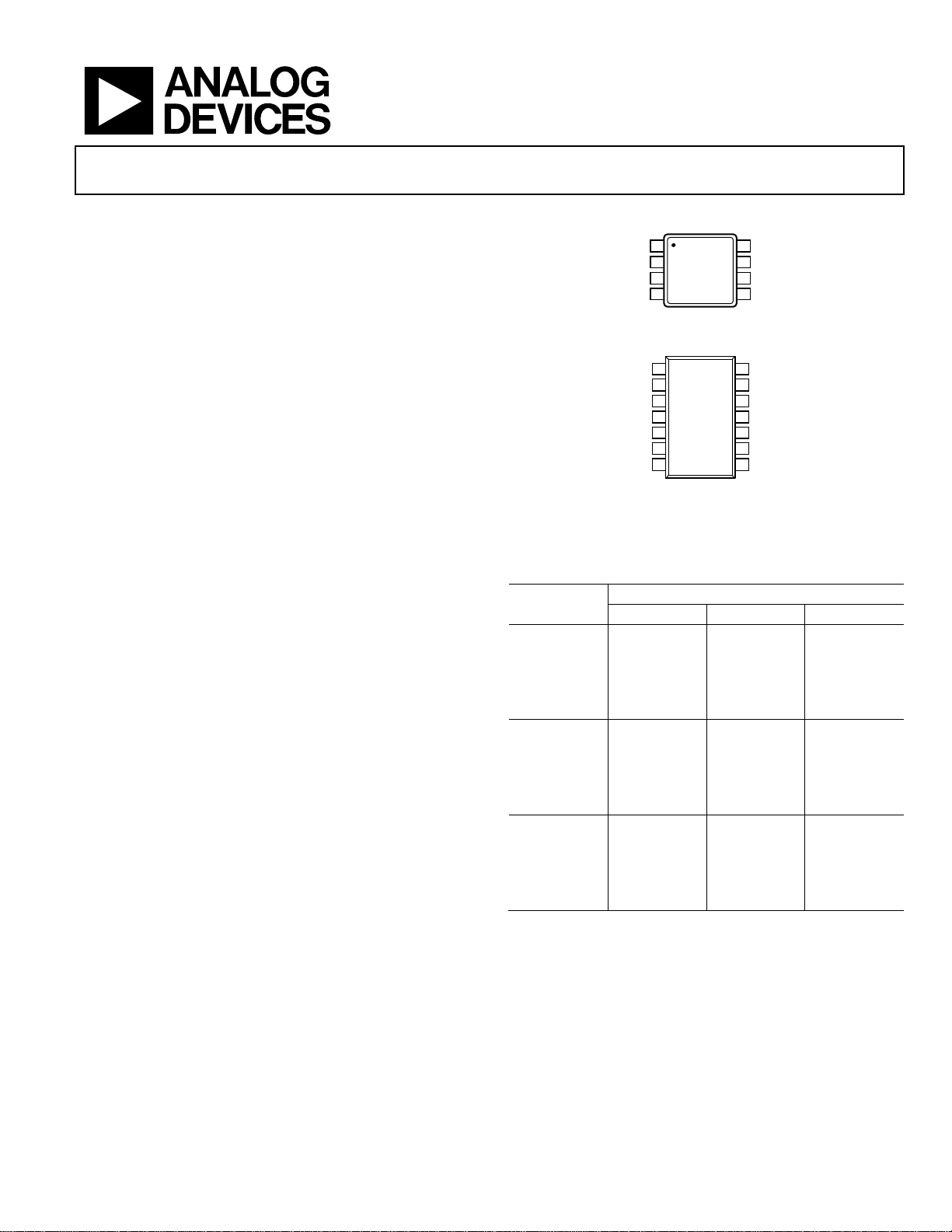
PIN CONFIGURATIONS
OUT A
1
AD8546
2
–IN A
+IN A
V–
TOP VIEW
3
(Not to Scale)
4
Figure 1. AD8546 (8-Lead MSOP)
OUT A
1
2
–IN A
+IN A
3
AD8548
4
V+
TOP VIEW
(Not to Scale)
+IN B
5
6
–IN B
OUT B
7
Figure 2. AD8548 (14-Lead SOIC_N)
Table 1. Micropower Op Amps
Amplifier
5 V 12 V to 18 V 36 V
Single AD8500 AD8663
AD8505
AD8541
AD8603
ADA4505-1
Dual AD8502 AD8546 OP295
AD8506 AD8657 ADA4062-2
AD8542 AD8667
AD8607 OP281
ADA4505-2
Quad AD8504 AD8548 OP495
AD8508 AD8669 ADA4062-4
AD8544 OP481
AD8609
ADA4505-4
1
See www.analog.com for the latest selection of micropower op amps.
V+
8
7
OUT B
–IN B
6
+IN B
5
OUT D
14
13
–IN D
+IN D
12
11
V–
+IN C
10
9
–IN C
OUT C
8
1
09585-103
Supply Voltage
09585-001
Rev. B
Information furnished by Analog Devices is believed to be accurate and reliable. However, no
responsibility is assumed by Analog Devices for its use, nor for any infringements of patents or other
rights of third parties that may result from its use. Specifications subject to change without notice. No
license is granted by implication or otherwise under any patent or patent rights of Analog Devices.
Trademarks and registered trademarks are the property of their respective owners.
One Technology Way, P.O. Box 9106, Norwood, MA 02062-9106, U.S.A.
Tel: 781.329.4700 www.analog.com
Fax: 781.461.3113 ©2011–2012 Analog Devices, Inc. All rights reserved.
Page 2

AD8546/AD8548 Data Sheet
TABLE OF CONTENTS
Features .............................................................................................. 1
Applications ....................................................................................... 1
Pin Configurations ........................................................................... 1
General Description ......................................................................... 1
Revision History ............................................................................... 2
Specifications ..................................................................................... 3
Electrical Characteristics—18 V Operation ............................. 3
Electrical Characteristics—10 V Operation ............................. 4
Electrical Characteristics—2.7 V Operation ............................ 5
Absolute Maximum Ratings ............................................................ 6
Thermal Resistance ...................................................................... 6
ESD Caution .................................................................................. 6
REVISION HISTORY
4/12—Rev. A to Rev. B
Added AD8548 and 14-Lead SOIC .................................. Universal
Changes to Product Title, Features Section, General
Description Section, and Table 1 .................................................... 1
Added Figure 2; Renumbered Figures Sequentially ..................... 1
Moved Electrical Characteristics—18 V Operation Section ...... 3
Changes to Table 2 ............................................................................ 3
Changes to Table 3 ............................................................................ 4
Moved Electrical Characteristics—2.7 V Operation Section ..... 5
Changes to Table 4 ............................................................................ 5
Changes to Table 6 ............................................................................ 6
Changes to Figure 4, Figure 5, Figure 7, and Figure 8 ................. 7
Deleted Figure 8 and Figure 11 ....................................................... 8
Typical Performance Characteristics ..............................................7
Applications Information .............................................................. 17
Input Stage ................................................................................... 17
Output Stage ................................................................................ 18
Rail-to-Rail Input and Output .................................................. 18
Resistive Load ............................................................................. 18
Comparator Operation .............................................................. 19
4 mA to 20 mA Process Control Current Loop Transmitter .. 20
Outline Dimensions ....................................................................... 21
Ordering Guide .......................................................................... 21
Changes to Figure 9, Figure 10, Figure 12, and Figure 13 ............ 8
Changes to Figure 22 and Figure 25 ............................................ 10
Changes to Figure 33 ...................................................................... 12
Changes to Figure 63 and Figure 64 ............................................ 18
Updated Outline Dimensions ....................................................... 21
Added Figure 72 ............................................................................. 21
Changes to Ordering Guide .......................................................... 21
4/11—Rev. 0 to Rev. A
Changes to Product Title, Features Section, Applications
Section, General Description Section, and Table 1 ....................... 1
1/11—Revision 0: Initial Version
Rev. B | Page 2 of 24
Page 3

Data Sheet AD8546/AD8548
−40°C ≤ TA ≤ +125°C
105
dB
INDM
INCM
OUT
Power Supply Rejection Ratio
PSRR
VSY = 2.7 V to 18 V
95
115 dB
Voltage Noise
en p-p
f = 0.1 Hz to 10 Hz
5
µV p-p
SPECIFICATIONS
ELECTRICAL CHARACTERISTICS—18 V OPERATION
VSY = 18 V, VCM = VSY/2, TA = 25°C, unless otherwise noted.
Table 2.
Parameter Symbol Test Conditions/Comments Min Typ Max Unit
INPUT CHARACTERISTICS
Offset Voltage VOS VCM = 0 V to 18 V 3 mV
VCM = 0.3 V to 17.7 V; −40°C ≤ TA ≤ +125°C 7 mV
VCM = 0 V to 18 V; −40°C ≤ TA ≤ +125°C 12 mV
Offset Voltage Drift ΔVOS/ΔT 3 µV/°C
Input Bias Current IB 5 20 pA
−40°C ≤ TA ≤ +125°C 2.6 nA
Input Offset Current IOS 40 pA
−40°C ≤ TA ≤ +125°C 5.2 nA
Input Voltage Range IVR 0 18 V
Common-Mode Rejection Ratio CMRR VCM = 0 V to 18 V 74 95 dB
VCM = 0.3 V to 17.7 V; −40°C ≤ TA ≤ +125°C 68 dB
VCM = 0 V to 18 V; −40°C ≤ TA ≤ +125°C 65 dB
Large Signal Voltage Gain AVO RL = 100 kΩ; VO = 0.5 V to 17.5 V 110 125 dB
Input Resistance RIN 10 GΩ
Input Capacitance
Differential Mode C
Common Mode C
OUTPUT CHARACTERISTICS
Output Voltage High VOH RL = 100 kΩ to VCM; −40°C ≤ TA ≤ +125°C 17.97 V
Output Voltage Low VOL RL = 100 kΩ to VCM; −40°C ≤ TA ≤ +125°C 30 mV
Short-Circuit Current ISC ±12 mA
Closed-Loop Output Impedance Z
POWER SUPPLY
−40°C ≤ TA ≤ +125°C 90 dB
Supply Current per Amplifier ISY IO = 0 mA 18 22 µA
−40°C ≤ TA ≤ +125°C 33 µA
DYNAMIC PERFORMANCE
Slew Rate SR RL = 1 MΩ; CL = 10 pF; AV = +1 80 V/ms
Settling Time to 0.1% tS VIN = 1 V step; RL = 100 kΩ; CL = 10 pF 15 µs
Gain Bandwidth Product GBP RL = 1 MΩ; CL = 10 pF; AV = +1 240 kHz
Phase Margin ΦM RL = 1 MΩ; CL = 10 pF; AV = +1 60 Degrees
Channel Separation CS f = 10 kHz; RL = 1 MΩ 105 dB
NOISE PERFORMANCE
Voltage Noise Density en f = 1 kHz 50 nV/√Hz
f = 10 kHz 45 nV/√Hz
Current Noise Density in f = 1 kHz 0.1 pA/√Hz
3.5 pF
10.5 pF
f = 1 kHz; AV = +1 15 Ω
Rev. B | Page 3 of 24
Page 4

AD8546/AD8548 Data Sheet
Input Resistance
RIN
10 GΩ
INDM
INCM
OUT
ELECTRICAL CHARACTERISTICS—10 V OPERATION
VSY = 10 V, VCM = VSY/2, TA = 25°C, unless otherwise noted.
Table 3.
Parameter Symbol Test Conditions/Comments Min Typ Max Unit
INPUT CHARACTERISTICS
Offset Voltage VOS VCM = 0 V to 10 V 3 mV
VCM = 0.3 V to 9.7 V; −40°C ≤ TA ≤ +125°C 8 mV
VCM = 0 V to 10 V; −40°C ≤ TA ≤ +125°C 12 mV
Offset Voltage Drift ΔVOS/ΔT 3 µV/°C
Input Bias Current IB 2 15 pA
−40°C ≤ TA ≤ +125°C 2.6 nA
Input Offset Current IOS 30 pA
−40°C ≤ TA ≤ +125°C 5.2 nA
Input Voltage Range IVR 0 10 V
Common-Mode Rejection Ratio CMRR VCM = 0 V to 10 V 70 88 dB
VCM = 0.3 V to 9.7 V; −40°C ≤ TA ≤ +125°C 62 dB
VCM = 0 V to 10 V; −40°C ≤ TA ≤ +125°C 60 dB
Large Signal Voltage Gain AVO RL = 100 kΩ; VO = 0.5 V to 9.5 V 105 120 dB
−40°C ≤ TA ≤ +125°C 100 dB
Input Capacitance
Differential Mode C
Common Mode C
OUTPUT CHARACTERISTICS
Output Voltage High VOH RL = 100 kΩ to VCM; −40°C ≤ TA ≤ +125°C 9.98 V
Output Voltage Low VOL RL = 100 kΩ to VCM; −40°C ≤ TA ≤ +125°C 20 mV
Short-Circuit Current ISC ±11 mA
Closed-Loop Output Impedance Z
POWER SUPPLY
Power Supply Rejection Ratio PSRR VSY = 2.7 V to 18 V 95 115 dB
−40°C ≤ TA ≤ +125°C 90 dB
Supply Current per Amplifier ISY IO = 0 mA 18 22 µA
−40°C ≤ TA ≤ +125°C 33 µA
DYNAMIC PERFORMANCE
Slew Rate SR RL = 1 MΩ; CL = 10 pF; AV = +1 75 V/ms
Settling Time to 0.1% tS VIN = 1 V step; RL = 100 kΩ; CL = 10 pF 15 µs
Gain Bandwidth Product GBP RL = 1 MΩ; CL = 10 pF; AV = +1 235 kHz
Phase Margin ΦM RL = 1 MΩ; CL = 10 pF; AV = +1 60 Degrees
Channel Separation CS f = 10 kHz; RL = 1 MΩ 105 dB
NOISE PERFORMANCE
Voltage Noise en p-p f = 0.1 Hz to 10 Hz 5 µV p-p
Voltage Noise Density en f = 1 kHz 50 nV/√Hz
f = 10 kHz 45 nV/√Hz
Current Noise Density in f = 1 kHz 0.1 pA/√Hz
3.5 pF
3.5 pF
f = 1 kHz; AV = +1 15 Ω
Rev. B | Page 4 of 24
Page 5

Data Sheet AD8546/AD8548
Input Resistance
RIN
10 GΩ
INDM
INCM
OUT
ELECTRICAL CHARACTERISTICS—2.7 V OPERATION
VSY = 2.7 V, VCM = VSY/2, TA = 25°C, unless otherwise noted.
Table 4.
Parameter Symbol Test Conditions/Comments Min Typ Max Unit
INPUT CHARACTERISTICS
Offset Voltage VOS VCM = 0 V to 2.7 V 3 mV
VCM = 0.3 V to 2.4 V; −40°C ≤ TA ≤ +125°C 4 mV
VCM = 0 V to 2.7 V; −40°C ≤ TA ≤ +125°C 12 mV
Offset Voltage Drift ΔVOS/ΔT 3 µV/°C
Input Bias Current IB 1 10 pA
−40°C ≤ TA ≤ +125°C 2.6 nA
Input Offset Current IOS 20 pA
−40°C ≤ TA ≤ +125°C 5.2 nA
Input Voltage Range IVR 0 2.7 V
Common-Mode Rejection Ratio CMRR VCM = 0 V to 2.7 V 60 75 dB
VCM = 0.3 V to 2.4 V; −40°C ≤ TA ≤ +125°C 58 dB
VCM = 0 V to 2.7 V; −40°C ≤ TA ≤ +125°C 49 dB
Large Signal Voltage Gain AVO RL = 100 kΩ; VO = 0.5 V to 2.2 V 97 115 dB
−40°C ≤ TA ≤ +125°C 90 dB
Input Capacitance
Differential Mode C
Common Mode C
OUTPUT CHARACTERISTICS
Output Voltage High VOH RL = 100 kΩ to VCM; −40°C ≤ TA ≤ +125°C 2.69 V
Output Voltage Low VOL RL = 100 kΩ to VCM; −40°C ≤ TA ≤ +125°C 10 mV
Short-Circuit Current ISC ±4 mA
Closed-Loop Output Impedance Z
POWER SUPPLY
Power Supply Rejection Ratio PSRR VSY = 2.7 V to 18 V 95 115 dB
−40°C ≤ TA ≤ +125°C 90 dB
Supply Current per Amplifier ISY IO = 0 mA 18 22 µA
−40°C ≤ TA ≤ +125°C 33 µA
DYNAMIC PERFORMANCE
Slew Rate SR RL = 1 MΩ; CL = 10 pF; AV = +1 50 V/ms
Settling Time to 0.1% tS VIN = 1 V step; RL = 100 kΩ; CL = 10 pF 20 µs
Gain Bandwidth Product GBP RL = 1 MΩ; CL = 10 pF; AV = +1 190 kHz
Phase Margin ΦM RL = 1 MΩ; CL = 10 pF; AV = +1 60 Degrees
Channel Separation CS f = 10 kHz; RL = 1 MΩ 105 dB
NOISE PERFORMANCE
Voltage Noise en p-p f = 0.1 Hz to 10 Hz 6 µV p-p
Voltage Noise Density en f = 1 kHz 60 nV/√Hz
f = 10 kHz 56 nV/√Hz
Current Noise Density in f = 1 kHz 0.1 pA/√Hz
3.5 pF
3.5 pF
f = 1 kHz; AV = +1 20 Ω
Rev. B | Page 5 of 24
Page 6
AD8546/AD8548 Data Sheet
Input Voltage
(V−) − 300 mV to (V+) + 300 mV
Operating Temperature Range
−40°C to +125°C
Package Type
θJA
θJC
Unit
14-Lead SOIC_N (R-14)
115
36
°C/W
ABSOLUTE MAXIMUM RATINGS
Table 5.
Parameter Rating
Supply Voltage 20.5 V
Input Current1 ±10 mA
Differential Input Voltage ±VSY
Output Short-Circuit Duration
to GND
Storage Temperature Range −65°C to +150°C
Junction Temperature Range −65°C to +150°C
Lead Temperature
(Soldering, 60 sec)
1
The input pins have clamp diodes to the power supply pins. Limit the input
current to 10 mA or less whenever input signals exceed the power supply
rail by 0.3 V.
Indefinite
300°C
Stresses above those listed under Absolute Maximum Ratings
may cause permanent damage to the device. This is a stress
rating only; functional operation of the device at these or any
other conditions above those indicated in the operational
section of this specification is not implied. Exposure to absolute
maximum rating conditions for extended periods may affect
device reliability.
THERMAL RESISTANCE
θJA is specified for the worst-case conditions, that is, a device
soldered in a circuit board for surface-mount packages using
a standard 4-layer board.
Table 6. Thermal Resistance
8-Lead MSOP (RM-8) 142 45 °C/W
ESD CAUTION
Rev. B | Page 6 of 24
Page 7
Data Sheet AD8546/AD8548
0
5
10
15
20
25
30
35
40
–2.0
–1.8
–1.6
–1.4
–1.2
–2.4
–2.2
–1.0
–0.8
–0.6
–0.4
–0.2
0
0.2
0.4
0.6
0.8
1.0
1.2
1.4
1.6
1.8
2.0
2.2
2.4
NUMBER OF AMPLIFIERS
V
OS
(mV)
09585-002
VSY = 2.7V
V
CM
= VSY/2
0
10
20
30
40
50
60
70
0 0.5 1.0 1.5 2.0 2.5 3.0 3.5 4.0 4.5 5.0 5.5 6.0
NUMBER OF AMPLIFIERS
TCVOS (µV/°C)
V
SY
= 2.7V
–40°C ≤ T
A
≤ +125°C
09585-004
–3.0
–2.5
–2.0
–1.5
–1.0
–0.5
0
0.5
1.0
1.5
2.0
2.5
3.0
0 0.3 0.6 0.9 1.2 1.5 1.8 2.1 2.4 2.7
V
OS
(mV)
VCM (V)
VSY = 2.7V
09585-005
0
5
10
15
20
25
30
35
40
–2.0
–1.8
–1.6
–1.4
–1.2
–2.4
–2.2
–1.0
–0.8
–0.6
–0.4
–0.2
0
0.2
0.4
0.6
0.8
1.0
1.2
1.4
1.6
1.8
2.0
2.2
2.4
NUMBER OF AMPLIFIERS
V
OS
(mV)
09585-105
V
SY
= 18V
V
CM
= VSY/2
0
10
20
30
40
50
60
70
0 0.5 1.0 1.5 2.0 2.5 3.0 3.5 4.0 4.5 5.0 5.5 6.0
NUMBER OF AMPLIFIERS
TCV
OS
(µV/°C)
VSY = 18V
–40°C ≤ T
A
≤ +125°C
09585-007
–3.0
–2.5
–2.0
–1.5
–1.0
–0.5
0
0.5
1.0
1.5
2.0
2.5
3.0
0 2 4 6 8 10 12 14 16 18
V
OS
(mV)
VCM (V)
VSY = 18V
09585-008
TYPICAL PERFORMANCE CHARACTERISTICS
TA = 25°C, unless otherwise noted.
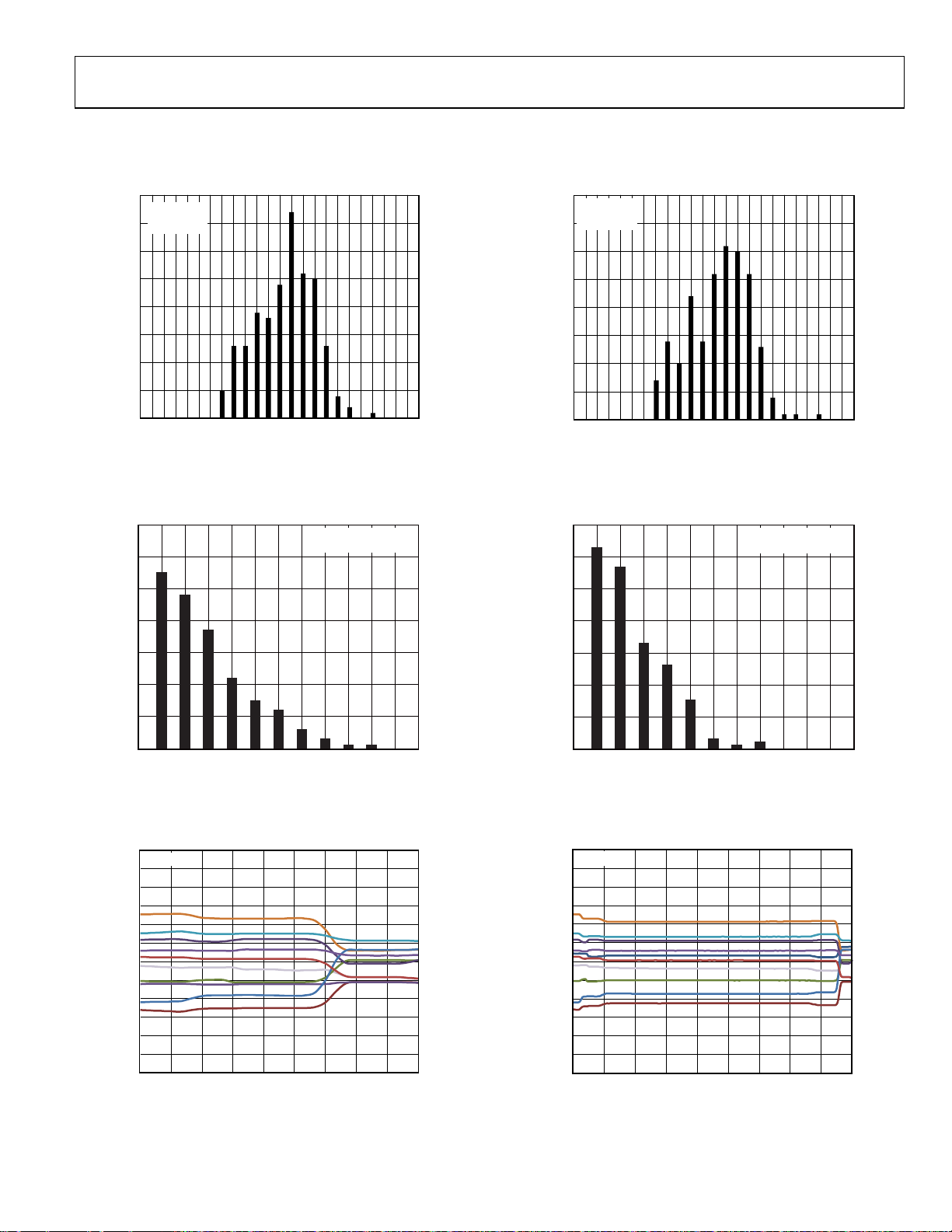
Figure 3. Input Offset Voltage Distribution
Figure 4. Input Offset Voltage Drift Distribution
Figure 6. Input Offset Voltage Distribution
Figure 7. Input Offset Voltage Drift Distribution
Figure 5. Input Offset Voltage vs. Common-Mode Voltage
Figure 8. Input Offset Voltage vs. Common-Mode Voltage
Rev. B | Page 7 of 24
Page 8
AD8546/AD8548 Data Sheet
–6
–4
–2
0
2
4
6
0 0.3 0.6 0.9 1.2 1.5 1.8 2.1 2.4 2.7
V
OS
(mV)
VCM (V)
VSY = 2.7V
–40°C ≤ T
A
≤ +125°C
09585-110
0.1
1
10
100
1000
10000
25 50 75 100 125
I
B
(pA)
TEMPERATURE (°C)
| IB+ |
| IB– |
VSY = 2.7V
09585-010
–4
–3
–2
–1
0
1
2
3
4
0 0.3 0.6 0.9 1.2 1.5 1.8 2.1 2.4 2.7
I
B
(nA)
VCM (V)
25°C
85°C
125°C
VSY = 2.7V
09585-014
–6
–4
–2
0
2
4
6
0 3 6 9 12 15
18
V
OS
(mV)
VCM (V)
V
SY
= 18V
–40°C ≤ T
A
≤ +125°C
09585-113
0.1
1
10
100
1000
10000
25 50 75 100 125
I
B
(pA)
TEMPERATURE (°C)
VSY = 18V
09585-013
| IB+ |
| IB– |
0 2 4 6 8 10 12 14 16 18
V
CM
(V)
25°C
85°C
125°C
VSY = 18V
09585-017
–4
–3
–2
–1
0
1
2
3
4
I
B
(nA)
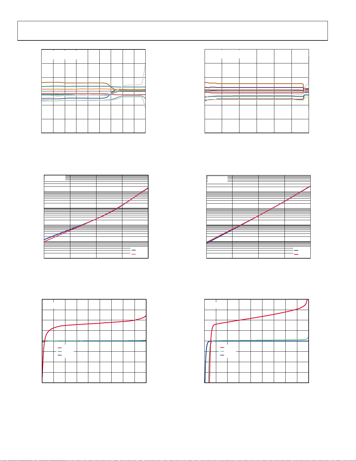
Figure 9. Input Offset Voltage vs. Common-Mode Voltage
Figure 10. Input Bias Current vs. Temperature
Figure 12. Input Offset Voltage vs. Common-Mode Voltage
Figure 13. Input Bias Current vs. Temperature
Figure 11. Input Bias Current vs. Common-Mode Voltage
Figure 14. Input Bias Current vs. Common-Mode Voltage
Rev. B | Page 8 of 24
Page 9

Data Sheet AD8546/AD8548
0.01m
0.1m
1m
10m
100m
1
10
0.001 0.01 0.1 1 10 100
OUTPUT VOLTAGE (V
OH
) TO SUPPLY RAIL (V)
LOAD CURRENT ( mA)
–40°C
+25°C
+85°C
+125°C
V
SY
= 2.7V
09585-015
0.01m
0.1m
1m
10m
100m
1
10
0.001 0.01 0.1 1 10 100
OUTPUT VOLTAGE (V
OL
) TO SUPPLY RAIL (V)
LOAD CURRENT ( mA)
–40°C
+25°C
+85°C
+125°C
V
SY
= 2.7V
09585-016
2.695
2.696
2.697
2.698
2.699
2.700
–50 –25 0 25 50 75 100 125
OUTPUT VOLTAGE, V
OH
(V)
TEMPERATURE (°C)
RL = 100kΩ
RL = 1MΩ
VSY = 2.7V
09585-020
0.01m
0.1m
1m
10m
100m
1
10
OUTPUT VOLTAGE (V
OH
) TO SUPPLY RAIL (V)
LOAD CURRENT ( mA)
–40°C
+25°C
+85°C
+125°C
VSY = 18V
0.001 0.01 0.1 1 10 100
09585-018
0.01m
0.1m
1m
10m
100m
1
10
0.001 0.01 0.1 1 10 100
OUTPUT VOLTAGE (V
OL
)
TO SUPPLY RAI L (V)
LOAD CURRENT ( mA)
–40°C
+25°C
+85°C
+125°C
V
SY
= 18V
09585-019
17.975
17.980
17.985
17.990
17.995
18.000
–50 –25 0 25 50 75 100 125
OUTPUT VOLTAGE, V
OH
(V)
TEMPERATURE (°C)
RL = 100kΩ
R
L
= 1MΩ
V
SY
= 18V
09585-023
Figure 15. Output Voltage (VOH) to Supply Rail vs. Load Current
Figure 16. Output Voltage (VOL) to Supply Rail vs. Load Current
Figure 18. Output Voltage (VOH) to Supply Rail vs. Load Current
Figure 19. Output Voltage (VOL) to Supply Rail vs. Load Current
Figure 17. Output Voltage (VOH) vs. Temperature
Figure 20. Output Voltage (VOH) vs. Temperature
Rev. B | Page 9 of 24
Page 10

AD8546/AD8548 Data Sheet
0
1
2
3
4
5
6
–50 –25 0 25 50
75 100 125
OUTPUT VOLTAGE, V
OL
(mV)
TEMPERATURE (°C)
V
SY
= 2.7V
09585-021
R
L
= 100kΩ
R
L
= 1MΩ
0
5
10
15
20
25
30
35
0 0.3 0.6 0.9 1.2 1.5 1.8 2.1 2.4 2.7
I
SY
PER AMP (µA)
V
CM
(V)
–40°C
+25°C
+85°C
+125°C
V
SY
= 2.7V
09585-123
0
5
10
15
20
25
30
35
0 3 6 9 12 15 18
I
SY
PER AMP (µA)
VSY (V)
–40°C
+25°C
+85°C
+125°C
09585-026
0
2
4
6
8
10
12
–50 –25 0 25 50 75 100 125
OUTPUT VOLTAGE, V
OL
(mV)
TEMPERATURE (°C)
09585-024
R
L
= 100kΩ
R
L
= 1MΩ
V
SY
= 18V
0
5
10
15
20
25
30
35
0 3 6 9 12 15 18
I
SY
PER AMP (µA)
V
CM
(V)
V
SY
= 18V
–40°C
+25°C
+85°C
+125°C
09585-126
0
10
20
30
40
50
60
–50 –25 0 25
50 75 100 125
I
SY
PER AMP (µA)
TEMPERATURE (°C)
VSY = 2.7V
V
SY
= 18V
09585-029
Figure 21. Output Voltage (VOL) vs. Temperature
Figure 22. Supply Current per Amplifier vs. Common-Mode Voltage
Figure 24. Output Voltage (VOL) vs. Temperature
Figure 25. Supply Current per Amplifier vs. Common-Mode Voltage
Figure 23. Supply Current per Amplifier vs. Supply Voltage
Figure 26. Supply Current per Amplifier vs. Temperature
Rev. B | Page 10 of 24
Page 11

Data Sheet AD8546/AD8548
–135
–90
–45
0
45
90
135
–60
–20
–40
0
20
40
60
1k 10k 100k 1M
PHASE (Degrees)
OPEN-LOOP GAIN (dB)
FREQUENCY (Hz)
PHASE
GAIN
09585-027
CL = 10pF
CL = 100pF
VSY = 2.7V
R
L
= 1MΩ
–60
–40
–20
0
20
40
60
100 1k 10k 100k 1M
CLOSED-LOOP GAI N ( dB)
FREQUENCY (Hz)
V
SY
= 2.7V
A
V
= +100
A
V
= +10
A
V
= +1
09585-028
1
10
100
1000
100 1k
10k 100k
Z
OUT
(Ω)
FREQUENCY (Hz)
VSY = 2.7V
A
V
= +1
A
V
= +10
A
V
= +100
09585-032
1k 10k 100k 1M
OPEN-LOOP GAIN (dB)
FREQUENCY (Hz)
09585-030
PHASE
–135
–90
–45
0
45
90
135
–60
–20
–40
0
20
40
60
GAIN
PHASE (Degrees)
CL = 10pF
CL = 100pF
VSY = 18V
R
L
= 1MΩ
–60
–40
–20
0
20
40
60
100 1k 10k 100k 1M
CLOSED-LOOP GAI N ( dB)
FREQUENCY (Hz)
VSY = 18V
AV = +100
AV = +10
A
V
= +1
09585-031
1
10
100
1000
100 1k 10k 100k
Z
OUT
(Ω)
FREQUENCY (Hz)
VSY = 18V
09585-035
AV = +1
A
V
= +10
A
V
= +100
Figure 27. Open-Loop Gain and Phase vs. Frequency
Figure 28. Closed-Loop Gain vs. Frequency
Figure 30. Open-Loop Gain and Phase vs. Frequency
Figure 31. Closed-Loop Gain vs. Frequency
Figure 29. Output Impedance vs. Frequency
Figure 32. Output Impedance vs. Frequency
Rev. B | Page 11 of 24
Page 12

AD8546/AD8548 Data Sheet
0
20
40
60
80
100
120
140
100 1k 10k 100k 1M
CMRR (dB)
FREQUENCY (Hz)
V
SY
= 2.7V
V
CM
= VSY/2
09585-134
0
20
40
60
80
100
100 1k 10k 100k 1M
PSRR (dB)
FREQUENCY (Hz)
PSRR+
PSRR–
VSY = 2.7V
09585-034
0
10
20
30
40
50
60
70
10 100 1000
OVERSHOOT (%)
CAPACITANCE (pF)
09585-038
VSY = 2.7V
V
IN
= 10mV p-p
R
L
= 1MΩ
OS+
OS–
100 1k 10k 100k 1M
CMRR (dB)
FREQUENCY (Hz)
VSY = 18V
V
CM
= VSY/2
0
20
40
60
80
100
120
140
09585-036
0
20
40
60
80
100
100 1k 10k 100k 1M
PSRR (dB)
FREQUENCY (Hz)
PSRR+
PSRR–
V
SY
= 18V
09585-037
0
10
20
30
40
50
60
70
10 100 1000
OVERSHOOT (%)
CAPACITANCE (pF)
OS+
OS–
09585-041
VSY = 18V
V
IN
= 10mV p-p
R
L
= 1MΩ
Figure 33. CMRR vs. Frequency
Figure 34. PSRR vs. Frequency
Figure 36. CMRR vs. Frequency
Figure 37. PSRR vs. Frequency
Figure 35. Small Signal Overshoot vs. Load Capacitance
Figure 38. Small Signal Overshoot vs. Load Capacitance
Rev. B | Page 12 of 24
Page 13

Data Sheet AD8546/AD8548
TIME (100µ s/DIV)
VOLTAGE (500mV/DIV )
VSY = ±1.35V
A
V
= +1
R
L
= 1MΩ
C
L
= 100pF
09585-039
TIME (100µ s/DIV)
VOLTAGE (5mV/DIV)
VSY = ±1.35V
A
V
= +1
R
L
= 1MΩ
C
L
= 100pF
09585-040
TIME (40µ s/DIV)
–0.4
–0.2
0
2
1
0
INPUT VOLTAGE (V)
OUTPUT VOLTAGE (V)
VSY = ±1.35V
A
V
= –10
R
L
= 1MΩ
INPUT
OUTPUT
09585-044
TIME (100µ s/DIV)
VOLTAGE (5V/DIV)
VSY = ±9V
A
V
= +1
R
L
= 1MΩ
C
L
= 100pF
09585-042
TIME (100µ s/DIV)
VOLTAGE (5mV/DIV)
09585-043
VSY = ±9V
A
V
= +1
R
L
= 1MΩ
C
L
= 100pF
TIME (40µ s/DIV)
–1
0
–2
10
5
0
INPUT VOLTAGE (V)
OUTPUT VOLTAGE (V)
VSY = ±9V
A
V
= –10
R
L
= 1MΩ
INPUT
OUTPUT
09585-047
Figure 39. Large Signal Transient Response
Figure 40. Small Signal Transient Response
Figure 42. Large Signal Transient Response
Figure 43. Small Signal Transient Response
Figure 44. Positive Overload Recovery
Rev. B | Page 13 of 24
Figure 41. Positive Overload Recovery
Page 14

AD8546/AD8548 Data Sheet
TIME (40µ s/DIV)
0
0.2
0.4
0
–1
–2
INPUT VOLTAGE (V)
OUTPUT VOLTAGE (V)
V
SY
= ±1.35V
A
V
= –10
R
L
= 1MΩ
INPUT
OUTPUT
09585-045
TIME (10µ s/DIV)
0
+5mV
–5mV
VOLTAGE (500mV/DIV )
VSY = 2.7V
R
L
= 100kΩ
C
L
= 10pF
INPUT
OUTPUT
ERROR BAND
09585-046
TIME (10µ s/DIV)
0
+5mV
–5mV
VOLTAGE (500mV/DIV )
VSY = 2.7V
R
L
= 100kΩ
C
L
= 10pF
INPUT
OUTPUT
ERROR BAND
09585-050
TIME (40µ s/DIV)
0
1
2
0
–5
–10
INPUT VOLTAGE (V)
OUTPUT VOLTAGE (V)
V
SY
= ±9V
A
V
= –10
R
L
= 1MΩ
INPUT
OUTPUT
09585-048
TIME (10µ s/DIV)
0
+5mV
–5mV
VOLTAGE (500mV/DIV )
V
SY
= 18V
R
L
= 100kΩ
C
L
= 10pF
INPUT
OUTPUT
ERROR BAND
09585-049
TIME (10µ s/DIV)
0
+5mV
–5mV
VOLTAGE (500mV/DIV )
VSY = 18V
R
L
= 100kΩ
C
L
= 10pF
INPUT
OUTPUT
ERROR BAND
09585-053
Figure 45. Negative Overload Recovery
Figure 46. Positive Settling Time to 0.1%
Figure 48. Negative Overload Recovery
Figure 49. Positive Settling Time to 0.1%
Figure 50. Negative Settling Time to 0.1%
Rev. B | Page 14 of 24
Figure 47. Negative Settling Time to 0.1%
Page 15

Data Sheet AD8546/AD8548
1
10
100
1000
10 100 1k 10k 100k 1M
VOLTAGE NOISE DENSITY (nV/ Hz)
FREQUENCY (Hz)
VSY = 2.7V
09585-051
TIME (2s/DIV)
VOLTAGE (2µV/DIV)
V
SY
= 2.7V
09585-052
0
0.5
1.0
1.5
2.0
2.5
3.0
10 100 1k 10k 100k 1M
OUTPUT SWING (V)
FREQUENCY (Hz)
09585-056
VSY = 2.7V
V
IN
= 2.6V
R
L
= 1MΩ
A
V
= +1
1
10
100
1000
10 100 1k
10k 100k 1M
VOLTAGE NOISE DENSITY (nV/
Hz)
FREQUENCY (Hz)
V
SY
= 18V
09585-054
TIME (2s/DIV)
VOLTAGE (2µV/DIV)
VSY = 18V
09585-055
10 100 1k 10k 100k 1M
OUTPUT SWING (V)
FREQUENCY (Hz)
0
2
4
6
8
10
12
14
16
18
20
09585-059
V
SY
= 18V
V
IN
= 17.9V
R
L
= 1MΩ
A
V
= +1
Figure 51. Voltage Noise Density vs. Frequency
Figure 52. 0.1 Hz to 10 Hz Noise
Figure 54. Voltage Noise Density vs. Frequency
Figure 55. 0.1 Hz to 10 Hz Noise
Figure 53. Output Swing vs. Frequency
Figure 56. Output Swing vs. Frequency
Rev. B | Page 15 of 24
Page 16

AD8546/AD8548 Data Sheet
0.01
0.1
1
10
100
10 100 1k 10k 100k
THD + N (%)
FREQUENCY (Hz)
09585-057
V
SY
= 2.7V
V
IN
= 0.2V rms
R
L
= 1MΩ
A
V
= +1
–140
–120
–100
–80
–60
–40
–20
0
100 1k 10k 100k
CHANNEL SEPARATION (dB)
FREQUENCY (Hz)
VIN = 0.5V p-p
V
IN
= 1.5V p-p
V
IN
= 2.6V p-p
09585-058
R
L
1MΩ
10kΩ
V
SY
= 2.7V
R
L
= 1MΩ
A
V
= –100
0.01
0.1
1
10
100
10 100 1k 10k 100k
THD + N (%)
FREQUENCY (Hz)
09585-060
V
SY
= 18V
V
IN
= 0.5V rms
R
L
= 1MΩ
A
V
= +1
–140
–120
–100
–80
–60
–40
–20
0
100 1k 10k 100k
CHANNEL SEPARATION (dB)
FREQUENCY (Hz)
VIN = 1V p-p
V
IN
= 5V p-p
V
IN
= 10V p-p
V
IN
= 15V p-p
V
IN
= 17V p-p
09585-061
R
L
1MΩ
10kΩ
VSY = 18V
R
L
= 1MΩ
A
V
= –100
Figure 57. THD + N vs. Frequency
Figure 58. Channel Separation vs. Frequency
Figure 59. THD + N vs. Frequency
Figure 60. Channel Separation vs. Frequency
Rev. B | Page 16 of 24
Page 17

Data Sheet AD8546/AD8548
V+
V–
+IN x
R1
D1 D2
M1 M2
M7 M6
M3 M4
M5
VB1
M8
M10
M9
M16
M17
M11
VB2
OUT x
M12
M14
M13
M15
I1
R2
–IN x
09585-062
APPLICATIONS INFORMATION
The AD8546/AD8548 are low input bias current, micropower
CMOS amplifiers that operate over a wide supply voltage range
of 2.7 V to 18 V. T he AD8546/AD8548 also employ unique input
and output stages to achieve rail-to-rail input and output ranges
with very low supply current.
INPUT STAGE
Figure 61 shows the simplified schematic of the AD8546/AD8548.
The input stage comprises two differential transistor pairs: an
NMOS pair (M1, M2) and a PMOS pair (M3, M4). The input
common-mode voltage determines which differential pair turns
on and is more active than the other.
The PMOS differential pair is active when the input voltage
approaches and reaches the lower supply rail. The NMOS differential pair is needed for input voltages up to and including the
upper supply rail. This topology allows the amplifier to maintain
a wide dynamic input voltage range and maximize signal swing to
both supply rails. For the greater part of the input common-mode
voltage range, the PMOS differential pair is active.
Differential pairs commonly exhibit different offset voltages.
The handoff from one pair to the other creates a step-like characteristic that is visible in the V
and Figure 8). This characteristic is inherent in all rail-to-rail
amplifiers that use the dual differential pair topology. Therefore,
always choose a common-mode voltage that does not include the
region of handoff from one input differential pair to the other.
Additional steps in the V
OS
input common-mode voltage approaches the power supply rails.
These changes are a result of the load transistors (M8, M9, M14,
and M15) running out of headroom. As the load transistors are
forced into the triode region of operation, the mismatch of their
vs. VCM graphs (see Figure 5
OS
vs. VCM graphs are also visible as the
drain impedances contributes to the offset voltage of the amplifier. This problem is exacerbated at high temperatures due to the
decrease in the threshold voltage of the input transistors. See
Figure 9 and Figure 12 for typical performance data.
Current Source I1 drives the PMOS transistor pair. As the input
common-mode voltage approaches the upper rail, I1 is steered
away from the PMOS differential pair through the M5 transistor.
The bias voltage, VB1, controls the point where this transfer occurs.
M5 diverts the tail current into a current mirror consisting of the
M6 and M7 transistors. The output of the current mirror then
drives the NMOS transistor pair. Note that the activation of this
current mirror causes a slight increase in supply current at high
common-mode voltages (see Figure 22 and Figure 25).
The AD8546/AD8548 achieve their high performance by using
low voltage MOS devices for their differential inputs. These low
voltage MOS devices offer excellent noise and bandwidth per unit
of current. Each differential input pair is protected by proprietary
regulation circuitry (not shown in Figure 61). The regulation
circuitry consists of a combination of active devices, which maintain the proper voltages across the input pairs during normal
operation, and passive clamping devices, which protect the
amplifier during fast transients. However, these passive clamping
devices begin to forward-bias as the common-mode voltage
approaches either power supply rail. This causes an increase in
the input bias current (see Figure 11 and Figure 14).
The input devices are also protected from large differential
input voltages by clamp diodes (D1 and D2). These diodes are
buffered from the inputs with two 10 kΩ resistors (R1 and R2).
The differential diodes turn on when the differential input voltage
exceeds approximately 600 mV; in this condition, the differential
input resistance drops to 20 kΩ.
Figure 61. Simplified Schematic
Rev. B | Page 17 of 24
Page 18

AD8546/AD8548 Data Sheet
TIME (200µ s/DIV)
VOLTAGE (5V/DIV)
VSY = ±9V
R
L
= 1MΩ
09585-063
INPUT
OUTPUT
AD8546/
AD8548
R1
R2
R
L
–V
SY
R
L, EFF
= R
L
|| R2
+V
SY
V
IN
V
OUT
09585-064
R1
R2
R
L
–V
SY
R
L, EFF
= RL|| (R1 + R2)
+V
SY
V
IN
V
OUT
09585-065
AD8546/
AD8548
OUTPUT STAGE
The AD8546/AD8548 feature a complementary output stage
consisting of the M16 and M17 transistors (see Figure 61). These
transistors are configured in a Class AB topology and are biased
by the voltage source, VB2. This topology allows the output voltage
to go within millivolts of the supply rails, achieving a rail-to-rail
output swing. The output voltage is limited by the output impedance of the transistors, which are low R
MOS devices. The output
ON
voltage swing is a function of the load current and can be estimated
using the output voltage to supply rail vs. load current graphs (see
Figure 15, Figure 16, Figure 18, and Figure 19).
RAIL-TO-RAIL INPUT AND OUTPUT
The AD8546/AD8548 feature rail-to-rail input and output with a
supply voltage from 2.7 V to 18 V. Figure 62 shows the input and
output waveforms of the AD8546/AD8548 configured as a unitygain buffer with a supply voltage of ±9 V and a resistive load of
1 MΩ. With an input voltage of ±9 V, the AD8546/AD8548 allow
the output to swing very close to both rails. Additionally, the
AD8546/AD8548 do not exhibit phase reversal.
RESISTIVE LOAD
The feedback resistor alters the load resistance that an amplifier
sees. Therefore, it is important to carefully select the value of the
feedback resistors used with the AD8546/AD8548. The amplifiers
are capable of driving resistive loads down to 100 kΩ. The Inverting
Op Amp Configuration section and the Noninverting Op Amp
Configuration section show how the feedback resistor changes
the actual load resistance seen at the output of the amplifier.
Inverting Op Amp Configuration
Figure 63 shows the AD8546/AD8548 in an inverting configuration with a resistive load, R
seen by the amplifier is the parallel combination of the feedback
resistor, R2, and the load, R
a feedback resistor of 1 kΩ and a load of 1 MΩ results in an
equivalent load resistance of 999 Ω at the output. Because the
AD8546/AD8548 are incapable of driving such a heavy load,
performance degrades greatly.
To avoid loading the output, use a larger feedback resistor, but
consider the effect of resistor thermal noise on the overall circuit.
, at the output. The actual load
L
. For example, the combination of
L
Figure 63. Inverting Op Amp Configuration
Noninverting Op Amp Configuration
Figure 64 shows the AD8546/AD8548 in a noninverting config-
Figure 62. Rail-to-Rail Input and Output
uration with a resistive load, R
by the amplifier is the parallel combination of R1 + R2 and R
, at the output. The actual load seen
L
.
L
Rev. B | Page 18 of 24
Figure 64. Noninverting Op Amp Configuration
Page 19

Data Sheet AD8546/AD8548
Ω
Ω
V
A
V
V
A
COMPARATOR OPERATION
An op amp is designed to operate in a closed-loop configuration
with feedback from its output to its inverting input. Figure 65
shows the AD8546 configured as a voltage follower with an input
voltage that is always kept at the midpoint of the power supplies.
The same configuration is applied to the unused channel. A1 and
A2 indicate the placement of ammeters to measure supply current.
I
+ refers to the current flowing from the upper supply rail to the
SY
op amp, and I
to the lower supply rail.
As expected, Figure 66 shows that in normal operating condition,
the total current flowing into the op amp is equivalent to the total
current flowing out of the op amp, where I
the AD8546 at V
40
35
30
25
20
L AMPLIFIER (µA)
15
PER DU
10
SY
I
Figure 66. Supply Current vs. Supply Voltage (Voltage Follower)
In contrast to op amps, comparators are designed to work in an
open-loop configuration and to drive logic circuits. Although
op amps are different from comparators, occasionally an unused
section of a dual or quad op amp is used as a comparator to save
board space and cost; however, this is not recommended.
Figure 67 and Figure 68 show the AD8546 configured as a comparator, with 100 kΩ resistors in series with the input pins. The
unused channel is configured as a buffer with the input voltage
kept at the midpoint of the power supplies.
− refers to the current owing from the op amp
SY
+
SY
A1
ISY+
100k
100k
AD8546
1/2
A2
–V
SY
ISY–
V
OUT
09585-066
Figure 65. Voltage Follower Configuration
+ = ISY− = 36 μA for
SY
= 18 V.
SY
ISY–
I
+
SY
5
0
024681012141618
VSY (V)
09585-067
+
SY
I
A1
+
1/2
–V
SY
V
OUT
ISY–
A2
SY
09585-068
100kΩ
AD8546
100kΩ
Figure 67. Comparator Configuration A
+
SY
I
A1
+
SY
100kΩ
100kΩ
AD8546
1/2
A2
–V
SY
ISY–
V
OUT
09585-069
Figure 68. Comparator Configuration B
The AD8546/AD8548 have input devices that are protected
from large differential input voltages by Diode D1 and Diode D2
(see Figure 61). These diodes consist of substrate PNP bipolar
transistors and turn on when the differential input voltage
exceeds approximately 600 mV; however, these diodes also allow
a current path from the input to the lower supply rail, resulting
in an increase in the total supply current of the system. As shown
in Figure 69, both configurations yield the same result. At 18 V
of power supply, I
I
− increases to 140 μA in magnitude per dual amplifier.
SY
160
140
120
100
80
LAMPLIFIER (µA)
60
PER DU
40
SY
I
20
0
024681012141618
Figure 69. Supply Current vs. Supply Voltage (AD8546 as a Comparator)
+ remains at 36 μA per dual amplifier, but
SY
ISY–
I
+
SY
VSY (V)
09585-070
Rev. B | Page 19 of 24
Page 20

AD8546/AD8548 Data Sheet
R
L
100Ω
V
DD
18V
C2
10µFC30.1µF
C1
390pF
C4
0.1µF
R4
3.3kΩ
Q1
D1
4mA
TO
20mA
R3
1.2kΩ
R
NULL
1MΩ
1%
V
REF
R
SPAN
200kΩ
1%
V
IN
0V TO 5V
R1
68kΩ
1%
R2
2kΩ
1%
NOTES
1. R1 + R2 = R´.
1/2
AD8546
C5
10µF
R
SENSE
100Ω
1%
09585-072
V
OUT
GND
ADR125
V
IN
Note that 100 kΩ resistors are used in series with the input of
the op amp. If smaller resistor values are used, the supply current
of the system increases much more. For more information about
using op amps as comparators, see the AN-849 Application Note,
Using Op Amps as Comparators.
4 mA TO 20 mA PROCESS CONTROL CURRENT LOOP TRANSMITTER
A 2-wire current transmitter is often used in distributed control
systems and process control applications to transmit analog signals
between sensors and process controllers. Figure 70 shows a 4 mA
to 20 mA current loop transmitter.
Figure 70. 4 mA to 20 mA Current Loop Transmitter
The transmitter is powered directly from the control loop
power supply, and the current in the loop carries signal from
4 mA to 20 mA. Thus, 4 mA establishes the baseline current
budget within which the circuit must operate.
The AD8546 is an excellent choice due to its low supply current
of 33 μA per amplifier over temperature and supply voltage. The
current transmitter controls the current flowing in the loop, where
a zero-scale input signal is represented by 4 mA of current and a
full-scale input signal is represented by 20 mA. The transmitter
also floats from the control loop power supply, V
, whereas signal
DD
ground is in the receiver. The loop current is measured at the load
resistor, R
With a zero-scale input, a current of V
R. This creates a current, I
, at the receiver side.
L
SENSE
REF/RNULL
flows through
, that flows through the sense
resistor, as determined by the following equation:
I
SENSE, MIN
= (V
× R)/(R
REF
NULL
× R
SENSE
)
With a full-scale input voltage, current flowing through R is
increased by the full-scale change in V
IN/RSPA N
. This creates an
increase in the current flowing through the sense resistor.
I
SENSE, DELTA
= (Full-Scale Change in VIN × R)/(R
SPAN
× R
SENSE
Therefore,
I
When R >> R
receiver side is almost equivalent to I
SENSE, MAX
= I
SENSE
SENSE, MIN
+ I
SENSE, DELTA
, the current through the load resistor at the
.
SENSE
Figure 70 shows a design for a full-scale input voltage of 5 V. At
0 V of input, the loop current is 3.5 mA, and at a full-scale input
of 5 V, th e l o o p current is 21 mA. This allows software calibration
to fine-tune the current loop to the 4 mA to 20 mA range.
Together, the AD8546 and the ADR125 consume quiescent
current of only 160 µA, making 3.34 mA current available to
power additional signal conditioning circuitry or to power a
bridge circuit.
)
Rev. B | Page 20 of 24
Page 21

Data Sheet AD8546/AD8548
COMPLIANT TO JEDEC STANDARDS MO-187-AA
6°
0°
0.80
0.55
0.40
4
815
0.65 BSC
0.40
0.25
1.10 MAX
3.20
3.00
2.80
COPLANARITY
0.10
0.23
0.09
3.20
3.00
2.80
5.15
4.90
4.65
PIN 1
IDENTIFIER
15° MAX
0.95
0.85
0.75
0.15
0.05
10-07-2009-B
CONTROLLING DIMENSIONS ARE IN MILLIME TERS; INCH DI M E NS IONS
(IN PARENTHESES) ARE ROUNDED-OFF MILLIMETER EQUIV
ALENTS FOR
REFERENCE O NLYAND ARE NOT APPROPRIATE FOR USE IN DESIGN.
COMPLIANT TO JEDEC S TANDARDS MS-012-AB
060606-A
14
8
7
1
6.20 (0.2441)
5.80 (0.2283)
4.00 (0.1575)
3.80 (0.1496)
8.75 (0.3445)
8.55 (0.3366)
1.27 (0.0500)
BSC
SEATING
PLANE
0.25 (0.0098)
0.10 (0.0039)
0.51 (0.0201)
0.31 (0.0122)
1.75 (0.0689)
1.35 (0.0531)
0.50 (0.0197)
0.25 (0.0098)
1.27 (0.0500)
0.40 (0.0157)
0.25 (0.0098)
0.17 (0.0067)
COPLANARITY
0.10
8°
0°
45°
OUTLINE DIMENSIONS
Figure 71. 8-Lead Mini Small Outline Package [MSOP]
(RM-8)
Dimensions shown in millimeters
Figure 72. 14-Lead Standard Small Outline Package [SOIC_N]
Narrow Body
(R-14)
Dimensions shown in millimeters and (inches)
ORDERING GUIDE
Model1 Temperature Range Package Description Package Option Branding
AD8546ARMZ −40°C to +125°C 8-Lead Mini Small Outline Package [MSOP] RM-8 A2V
AD8546ARMZ-RL −40°C to +125°C 8-Lead Mini Small Outline Package [MSOP] RM-8 A2V
AD8546ARMZ-R7 −40°C to +125°C 8-Lead Mini Small Outline Package [MSOP] RM-8 A2V
AD8548ARZ −40°C to +125°C 14-Lead Standard Small Outline Package [SOIC_N] R-14
AD8548ARZ-RL −40°C to +125°C 14-Lead Standard Small Outline Package [SOIC_N] R-14
AD8548ARZ-R7 −40°C to +125°C 14-Lead Standard Small Outline Package [SOIC_N] R-14
1
Z = RoHS Compliant Part.
Rev. B | Page 21 of 24
Page 22

AD8546/AD8548 Data Sheet
NOTES
Rev. B | Page 22 of 24
Page 23

Data Sheet AD8546/AD8548
NOTES
Rev. B | Page 23 of 24
Page 24

AD8546/AD8548 Data Sheet
©2011–2012 Analog Devices, Inc. All rights reserved. Trademarks and
NOTES
registered trademarks are the property of their respective owners.
D09585-0-4/12(B)
Rev. B | Page 24 of 24
 Loading...