

Page 1
8 MHz Rail-to-Rail
1
2
3
5
4
2IN A
+IN A
V+
OUT A
AD8519
V2
a
FEATURES
Space-Saving SOT-23, SOIC Packaging
Wide Bandwidth: 8 MHz @ 5 V
Low Offset Voltage: 1.2 mV Max
Rail-to-Rail Output Swing
2.7 V/s Slew Rate
Unity Gain Stable
Single Supply Operation: +2.7 V to +12 V
APPLICATIONS
Portable Communications
Microphone Amplifiers
Portable Phones
Sensor Interface
Active Filters
PCMCIA Cards
ASIC Input Drivers
Wearable Computers
Battery Powered Devices
Voltage Reference Buffers
Personal Digital Assistants
GENERAL DESCRIPTION
The AD8519 and AD8529 are rail-to-rail output bipolar amplifiers with a unity gain bandwidth of 8 MHz and a typical voltage
offset of less than 1 mV. The AD8519 brings precision and bandwidth to the SOT-23 package. The low supply current makes the
AD8519/AD8529 ideal for battery powered applications. The
rail-to-rail output swing of the AD8519/AD8529 is larger than
standard video op amps, making them useful in applications that
require greater dynamic range than standard video op amps. The
+2.7 V/µs slew rate makes the AD8529/AD8549 a good match
for driving ASIC inputs such as voice codecs.
The small SOT-23 package makes it possible to place the AD8519
next to sensors, reducing external noise pickup.
The AD8519/AD8529 is specified over the extended industrial
(–40°C to +125°C) temperature range. The AD8519 is avail-
able in 5-lead SOT-23-5 and SO-8 surface mount packages.
The AD8529 is available in 8-lead SOIC and µSOIC packages.
Operational Amplifiers
AD8519/AD8529
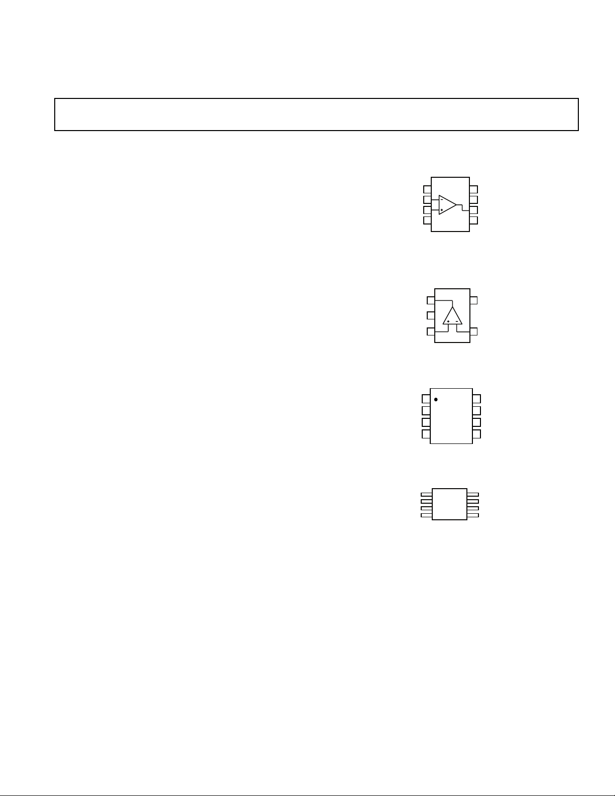
PIN CONFIGURATIONS
8-Lead SOIC
(R Suffix)
AD8519
NC
1
2IN A
2
+IN A
3
V2
4
NC = NO CONNECT
5-Lead SOT-23
(RT Suffix)
8-Lead SOIC
(R Suffix)
OUT A
18
AD8529
27
2IN A
1IN A
TOP VIEW
36
45
V2
8-Lead SOIC
(RM Suffix)
V2
1
AD8529
45
OUT A
2IN A
1IN A
NC
8
V+
7
OUT A
6
NC
5
V1
OUT B
2IN B
1IN B
8
V1
OUT B
2IN B
1IN B
REV. A
Information furnished by Analog Devices is believed to be accurate and
reliable. However, no responsibility is assumed by Analog Devices for its
use, nor for any infringements of patents or other rights of third parties
which may result from its use. No license is granted by implication or
otherwise under any patent or patent rights of Analog Devices.
One Technology Way, P.O. Box 9106, Norwood, MA 02062-9106, U.S.A.
Tel: 781/329-4700 World Wide Web Site: http://www.analog.com
Fax: 781/326-8703 © Analog Devices, Inc., 1998
Page 2

AD8519/AD8529–SPECIFICATIONS
ELECTRICAL CHARACTERISTICS
(VS = +5.0 V, V– = 0 V, VCM = +2.5 V, TA = +25ⴗC unless otherwise noted)
Parameter Symbol Conditions Min Typ Max Units
INPUT CHARACTERISTICS
Offset Voltage V
Offset Voltage V
Input Bias Current I
Input Offset Current I
Input Voltage Range V
OS
OS
B
OS
CM
Common-Mode Rejection Ratio CMRR 0 V ≤ V
Large Signal Voltage Gain A
Offset Voltage Drift ∆V
VO
/∆T2µV/°C
OS
AD8519ART (SOT-23-5) 600 1,100 µV
–40°C ≤ T
≤ +125°C 800 1,300 µV
A
AD8519AR (SO-8), AD8529 600 1,000 µV
–40°C ≤ T
≤ +125°C 1,100 µV
A
300 nA
–40°C ≤ T
≤ +125°C 400 nA
A
±50 nA
–40°C ≤ T
≤ +125°C ±100 nA
A
0+4V
≤ +4.0 V,
CM
–40°C ≤ T
R
= 2 kΩ, +0.5 V < V
L
= 10 kΩ, +0.5 V < V
R
L
= 10 kΩ, –40°C ≤ TA ≤ +125°C 30 V/mV
R
L
≤ +125°C 63 100 dB
A
< +4.5 V 30 V/mV
OUT
< +4.5 V 50 100 V/mV
OUT
Bias Current Drift ∆IB/∆T 500 pA/°C
OUTPUT CHARACTERISTICS
Output Voltage Swing High V
Output Voltage Swing Low V
Short Circuit Current I
Maximum Output Current I
OH
OL
SC
OUT
I
= 250 µA
L
–40°C ≤ T
= 5 mA +4.80 V
I
L
I
= 250 µA
L
–40°C ≤ T
= 5 mA 200 mV
I
L
≤ +125°C +4.90 V
A
≤ +125°C80mV
A
Short to Ground, Instantaneous ±70 mA
±25 mA
POWER SUPPLY
Power Supply Rejection Ratio PSRR V
Supply Current/Amplifier I
SY
= +2.7 V to +7 V, 110 dB
S
–40°C ≤ T
V
OUT
≤ +125°C80dB
A
= +2.5 V 600 1,200 µA
–40°C ≤ TA ≤ +125°C 1,400 µA
DYNAMIC PERFORMANCE
Slew Rate SR +1 V < V
Settling Time t
S
To 0.01% 1,200 ns
< +4 V, R
OUT
= 10 kΩ 2.9 V/µs
L
Gain Bandwidth Product GBP 8 MHz
Phase Margin φ
m
60 Degrees
NOISE PERFORMANCE
Voltage Noise e
Voltage Noise Density e
Current Noise Density i
Specifications subject to change without notice.
p-p 0.1 Hz to 10 Hz 0.5 µV p-p
n
n
n
f = 1 kHz 7 nV/√Hz
f = 1 kHz 0.4 pA/√Hz
–2– REV. A
Page 3

AD8519/AD8529
ELECTRICAL CHARACTERISTICS
(VS = +3.0 V, V– = 0 V, VCM = +1.5 V, TA = +25ⴗC unless otherwise noted)
Parameter Symbol Conditions Min Typ Max Units
INPUT CHARACTERISTICS
Offset Voltage V
Input Bias Current I
Input Offset Current I
Input Voltage Range V
OS
V
OS
B
OS
CM
Common-Mode Rejection Ratio CMRR 0 V ≤ V
Large Signal Voltage Gain A
VO
AD8519ART (SOT-23-5) 700 1,200 µV
–40°C ≤ T
≤ +125°C 900 1,400 µV
A
AD8519AR (SO-8), AD8529 700 1,100 µV
–40°C ≤ T
≤ +125°C 1,200 µV
A
300 nA
±50 nA
0+2V
≤ +2.0 V,
CM
–40°C ≤ T
R
= 2 kΩ, +0.5 V < V
L
R
= 10 kΩ 20 30 V/mV
L
≤ +125°C5575dB
A
< +2.5 V 20 V/mV
OUT
OUTPUT CHARACTERISTICS
Output Voltage Swing High V
Output Voltage Swing Low V
OH
OL
I
= 250 µA +2.90 V
L
= 5 mA +2.80 V
I
L
I
= 250 µA 100 mV
L
IL = 5 mA 200 mV
POWER SUPPLY
Power Supply Rejection Ratio PSRR V
Supply Current/Amplifier I
SY
= +2.5 V to +7 V,
S
–40°C ≤ T
V
OUT
≤ +125°C6080dB
A
= +1.5 V 600 1,100 µA
–40°C ≤ TA ≤ +125°C 1,300 µA
DYNAMIC PERFORMANCE
Slew Rate SR R
Settling Time t
S
= 10 kΩ 1.5 V/µs
L
To 0.01% 2,000 ns
Gain Bandwidth Product GBP 6 MHz
Phase Margin φ
m
55 Degrees
NOISE PERFORMANCE
Voltage Noise Density e
Current Noise Density i
Specifications subject to change without notice.
n
n
f = 1 kHz 10 nV/√Hz
f = 1 kHz 0.4 pA/√Hz
–3–REV. A
Page 4

AD8519/AD8529–SPECIFICATIONS
ELECTRICAL CHARACTERISTICS
(VS = +2.7 V, V– = 0 V, VCM = +1.35 V, TA = +25ⴗC unless otherwise noted)
Parameter Symbol Conditions Min Typ Max Units
INPUT CHARACTERISTICS
Offset Voltage V
Input Bias Current I
Input Offset Current I
Input Voltage Range V
OS
V
OS
B
OS
CM
Common-Mode Rejection Ratio CMRR 0 V ≤ V
Large Signal Voltage Gain A
VO
AD8519ART (SOT-23-5) 700 1,400 µV
–40°C ≤ T
≤ +125°C 900 1,600 µV
A
AD8519AR (SO-8), AD8529 700 1,200 µV
–40°C ≤ T
≤ +125°C 1,300 µV
A
300 nA
±50 nA
0+2V
≤ +1.7 V,
CM
–40°C ≤ T
R
= 2 kΩ, +0.5 V < V
L
R
= 10 kΩ 20 30 V/mV
L
≤ +125°C5575dB
A
< +2.2 V 20 V/mV
OUT
OUTPUT CHARACTERISTICS
Output Voltage Swing High V
Output Voltage Swing Low V
OH
OL
I
= 250 µA +2.60 V
L
= 5 mA +2.50 V
I
L
I
= 250 µA 100 mV
L
IL = 5 mA 200 mV
POWER SUPPLY
Power Supply Rejection Ratio PSRR V
Supply Current/Amplifier I
SY
= +2.5 V to +7 V,
S
–40°C ≤ T
V
OUT
≤ +125°C6080dB
A
= +1.35 V 600 1,100 µA
–40°C ≤ TA ≤ +125°C 1,300 µA
DYNAMIC PERFORMANCE
Slew Rate SR R
Settling Time t
S
= 10 kΩ 1.5 V/µs
L
To 0.01% 2,000 ns
Gain Bandwidth Product GBP 6 MHz
Phase Margin φ
m
55 Degrees
NOISE PERFORMANCE
Voltage Noise Density e
Current Noise Density i
Specifications subject to change without notice.
n
n
f = 1 kHz 10 nV/√Hz
f = 1 kHz 0.4 pA/√Hz
–4– REV. A
Page 5

AD8519/AD8529
ELECTRICAL CHARACTERISTICS
(VS = +5.0 V, V– = –5 V, VCM = 0 V, TA = +25ⴗC unless otherwise noted)
Parameter Symbol Conditions Min Typ Max Units
INPUT CHARACTERISTICS
Offset Voltage V
Input Bias Current I
Input Offset Current I
Input Voltage Range V
OS
V
OS
B
OS
CM
Common-Mode Rejection Ratio CMRR –4.9 V ≤ V
Large Signal Voltage Gain A
Offset Voltage Drift ∆V
VO
/∆T2µV/°C
OS
AD8519ART (SOT-23-5) 600 1,100 µV
–40°C ≤ T
≤ +125°C 800 1,300 µV
A
AD8519AR (SO-8), AD8529 600 1,000 µV
–40°C ≤ T
≤ +125°C 1,100 µV
A
VCM = 0 V 300 nA
= 0 V, –40°C ≤ TA ≤ +125°C 400 nA
V
CM
V
= 0 V ±50 nA
CM
= 0 V, –40°C ≤ TA ≤ +125°C ±100 nA
V
CM
–5 +4 V
≤ +4.0 V,
CM
–40°C ≤ T
R
= 2 kΩ 30 V/mV
L
= 10 kΩ 50 200 V/mV
R
L
–40°C ≤ T
≤ +125°C 70 100 dB
A
≤ +125°C 25 V/mV
A
Bias Current Drift ∆IB/∆T 500 pA/°C
OUTPUT CHARACTERISTICS
Output Voltage Swing High V
Output Voltage Swing Low V
Short Circuit Current I
Maximum Output Current I
OH
OL
SC
OUT
I
= 250 µA
L
–40°C ≤ T
= 5 mA +4.80 V
I
L
I
= 250 µA
L
–40°C ≤ T
= 5 mA –4.80 V
I
L
≤ +125°C +4.90 V
A
≤ +125°C –4.90 V
A
Short to Ground, Instantaneous ±70 mA
±25 mA
POWER SUPPLY
Power Supply Rejection Ratio PSRR V
Supply Current/Amplifier I
SY
= ±1.5 V to ±6 V,
S
–40°C ≤ T
V
OUT
≤ +125°C 60 100 dB
A
= 0 V 600 1,200 µA
–40°C ≤ TA ≤ +125°C 1,400 µA
DYNAMIC PERFORMANCE
Slew Rate SR –4 V < V
Settling Time t
S
To 0.01% 1,000 ns
< +4 V, R
OUT
= 10 kΩ 2.9 V/µs
L
Gain Bandwidth Product GBP 8 MHz
Phase Margin φ
m
60 Degrees
NOISE PERFORMANCE
Voltage Noise Density e
Current Noise Density i
Specifications subject to change without notice.
n
n
f = 1 kHz 7 nV/√Hz
f = 1 kHz 0.4 pA/√Hz
–5–REV. A
Page 6

AD8519/AD8529
WARNING!
ESD SENSITIVE DEVICE
ABSOLUTE MAXIMUM RATINGS
Supply Voltage . . . . . . . . . . . . . . . . . . . . . . . . . . . . . . . . . ±6 V
Input Voltage
Differential Input Voltage
2
. . . . . . . . . . . . . . . . . . . . . . . . . . . . . . . . ±6 V
3
. . . . . . . . . . . . . . . . . . . . . . ±0.6 V
Internal Power Dissipation
SOT-23 (RT) . . . . . . . . . . . . . . . . . Observe Derating Curve
SOIC (R) . . . . . . . . . . . . . . . . . . . . Observe Derating Curve
µSOIC (RM) . . . . . . . . . . . . . . . . . Observe Derating Curve
Output Short-Circuit Duration . . . . . Observe Derating Curve
Storage Temperature Range
RT, S Packages . . . . . . . . . . . . . . . . . . . . –65°C to +150°C
Operating Temperature Range
AD8519, AD8529 . . . . . . . . . . . . . . . . . . –40°C to +125°C
Junction Temperature Range
RT, S Packages . . . . . . . . . . . . . . . . . . . . –65°C to +150°C
Lead Temperature Range (Soldering, 60 sec) . . . . . . . +300°C
NOTES
1
Stresses above those listed under Absolute Maximum Ratings may cause perma-
nent damage to the device. This is a stress rating only; functional operation of the
device at these or any other conditions above those listed in the operational sections
of this specification is not implied. Exposure to absolute maximum rating conditions for extended periods may affect device reliability.
2
For supply voltages less than ±6 V the input voltage is limited to less than or equal
to the supply voltage.
3
For differential input voltages greater than ±0.6 V the input current should be limited
to less than 5 mA to prevent degradation or destruction of the input devices.
1
Package Type
1
JA
JC
Units
5-Lead SOT-23 (RT) 230 146 °C/W
8-Lead SOIC (R) 158 43 °C/W
8-Lead µSOIC (RM) 210 45 °C/W
NOTE
1
θJA is specified for worst case conditions, i.e., θ
in circuit board for SOT-23 and SOIC packages.
is specified for device soldered
JA
ORDERING GUIDE
Temperature Package Package
Model Range Description Option
AD8519ART
1
–40°C to +125°C 5-Lead SOT-23 RT-5
AD8519AR –40°C to +125°C 8-Lead SOIC SO-8
AD8529AR –40°C to +125°C 8-Lead SOIC SO-8
AD8529ARM
NOTES
1
Available in 3,000 piece reels only.
2
Available in 2,500 piece reels only.
2
–40°C to +125°C 8-Lead µSOIC RM-8
CAUTION
ESD (electrostatic discharge) sensitive device. Electrostatic charges as high as 4000 V readily
accumulate on the human body and test equipment and can discharge without detection.
Although the AD8519/AD8529 features proprietary ESD protection circuitry, permanent damage may occur on devices subjected to high energy electrostatic discharges. Therefore, proper
ESD precautions are recommended to avoid performance degradation or loss of functionality.
–6– REV. A
Page 7

Typical Characteristics –
TEMPERATURE – 8C
SUPPLY CURRENT – mA
800
700
300
250 225
150
0 255075100125
600
500
400
VS = +10V
VS = +5V
VS = +2.7V, +3.0V
GAIN – dB
45
90
135
180
PHASE SHIFT – Degrees
FREQUENCY – Hz
230
100k
10
VS = +5V
T
A
= +258C
220
210
0
20
30
40
50
225
270
1M 10M 100M
GAIN
PHASE
FREQUENCY – Hz
PSRR – dB
1k 10k 10M100k 1M
0
VS = +5V
T
A
= +258C
10
20
30
40
50
60
70
80
90
+PSRR
2PSRR
AD8519/AD8529
60
VS = +5V
= +258C
T
A
50
40
30
20
QUANTITY AMPLIFIERS
10
0
21 20.6120.2
INPUT OFFSET VOLTAGE – mV
COUNT = 395 OP AMPS
0.2 0.6
Figure 1. Input Offset Voltage
Distribution
40
VS = +5V
0
T
= +258C
A
240
280
2120
2160
INPUT BIAS CURRENT – nA
2200
2240
01 5
COMMON-MODE VOLTAGE – Volts
234
Figure 4. Input Bias Current vs.
Common-Mode Voltage
600
550
500
SUPPLY CURRENT – mA
450
0
46810
212
SUPPLY VOLTAGE – Volts
Figure 2. Supply Current per
Amplifier vs. Supply Voltage
120
VS = +5V
100
80
60
40
COMMON MODE REJECTION – dB
20
01 5
COMMON-MODE VOLTAGE – Volts
23 4
Figure 5. Common-Mode Rejection
vs. Common-Mode Voltage
Figure 3. Supply Current per
Amplifier vs. Temperature
Figure 6. Open Loop Gain, Phase vs.
Frequency
60
40
20
0
220
CLOSED LOOP GAIN – dB
240
10k 100k 100M1M 10M
Figure 7. Closed Loop Gain vs.
Frequency
FREQUENCY – Hz
VS = +5V
R
= 830V
L
T
= +258C
A
CL 5pF
110
100
90
80
70
60
CMRR – dB
50
40
30
20
1k 10k 10M100k 1M
FREQUENCY – Hz
VS = +5V
T
= +258C
A
Figure 8. CMRR vs. Frequency
–7–REV. A
Figure 9. PSRR vs. Frequency
Page 8

AD8519/AD8529
FREQUENCY – Hz
MAXIMUM OUTPUT SWING – V p-p
10k 100k 1M 10M
4
5
0
3
2
VS = +5V
AVCC = 1
R
L
= 10kV
T
A
= +258C
CL = 15pF
1
DISTORTION < 1%
FREQUENCY – Hz
10 100
1k 10k
0
VS = +5V
T
A
= +258C
1
2
3
4
5
6
7
8
CURRENT NOISE DENSITY – pA/ Hz
20mV
500ns
VS = 62.5V
AVCC = 1
T
A
= +258C
C
L
= 100pF
R
L
= 10kV
60
VS = +5V
V
= +2.5V
CM
50
= 10kV
R
L
T
= +258C
A
V
= 650mV
40
IN
30
20
OVERSHOOT – %
10
+OS
0
10 100 1k
CAPACITANCE – pF
2OS
Figure 10. Overshoot vs. Capacitance
Load
300
VS = +5V
T
= +258C
A
250
200
AVCC = 10
150
100
OUTPUT IMPEDANCE – V
50
0
100k 1M 10M
FREQUENCY – Hz
AVCC = 1
Figure 13. Output Impedance vs.
Frequency
4
VS = +5V
3
T
= +258C
A
1
0
21
STEP SIZE – V
22
23
24
0 2.0
1%
0.1%
0.1%
1%
1.0
SETTLING TIME – ms
Figure 11. Settling Time vs. Step Size
80
VS = +5V
70
T
= +258C
A
60
50
40
30
20
10
VOLTAGE NOISE DENSITY – nV/ Hz
0
10 100
FREQUENCY – Hz
1k 10k
Figure 14. AD8519 Voltage Noise
Density
Figure 12. Output Swing vs.
Frequency
Figure 15. AD8519 Current Noise
Density
20mV
Figure 16. 0.1 Hz to 10 Hz Noise
VS = 62.5V
A
= 100kV
V
en = 0.4mV p-p
1s
VS = 62.5V
V
= +6V p-p
IN
A
= 1
V
1V
20ms
Figure 17. No Phase Reversal
–8– REV. A
Figure 18. Small Signal Transient
Response
Page 9

VS = 62.5V
AD8519
D1
1N914
R6
5kV
R1
10kV
V
IN
R4
10kV
R2
10kV
D2
1N914
R3
4.99kV
R5
10kV
V
OUT
R7
3.32kV
AD8519
U2
U1
VIRTUAL GROUND =
V
CC
2
NODE A
AVCC = 1
T
= +258C
A
CL = 100pF
AD8519/AD8529
500mV
Figure 19. Large Signal Transient Response
APPLICATIONS INFORMATION
Maximum Power Dissipation
The maximum power that can be safely dissipated by the AD8519/
AD8529 is limited by the associated rise in junction temperature.
The maximum safe junction temperature is +150°C for these
plastic packages. If this maximum is momentarily exceeded, proper
circuit operation will be restored as soon as the die temperature is
reduced. Operating the product in the “overheated” condition for
an extended period can result in permanent damage to the device.
Precision Full-Wave Rectifier
Slew Rate is probably the most underestimated parameter when
designing a precision rectifier. Yet without a good slew rate
large glitches will be generated during the period when both
diodes are off.
Let’s examine the operation of the basic circuit before considering slew rate further, U1 is set up to have two states of operation. D1 and D2 diodes switch the output between the two
states. State one is as an inverter with a gain of 1 and state two
is a simple unity gain buffer where the output is equal to the
value of the virtual ground. The virtual ground is the potential
present at the noninverting node of the U1. State one is active
when V
condition. If V
is larger than the virtual ground. D2 is on in this
IN
drops below virtual ground, D2 turns off and
IN
D1 turns on. This causes the output of U1 to simply buffer the
virtual ground and this configuration is state two. So, the function of U1, which results from these two states of operation, is a
half-wave inverter. The U2 function takes the inverted half-wave
at a gain of two and sums it into the original V
outputs a rectified full-wave.
VV V
=− <
OUT IN IN
50ms
wave, which
IN
−
1
20
Figure 20. Precision Full-Wave Rectifier
This type of rectifier can be very precise if the following electrical parameters are adhered to: First, all passive components
should be of tight tolerance, 1% resistors and 5% capacitors.
Second, if the application circuit requires high impedance (i.e.,
direct sensor interface), then an FET amplifier is probably a
better choice than the AD8519. Third, an amp such as the
AD8519, which has a great slew rate specification, will yield the
best result, because the circuit involves switching. Switching
glitches are caused when D1 and D2 are both momentarily off.
This condition occurs every time the input signal is equal to the
virtual ground potential. When this condition occurs the U1
stage is taken out of the V
ⴛ R5 ⴛ (R4储R1+R2+R3). Please note: node A should be
V
IN
inverted or virtual ground, but in this condition node A is a
V
IN
simply tracking V
. Given a sine wave input centered around
IN
equation and V
OUT
is equal to
OUT
virtual ground glitches are generated at the sharp negative peaks
of the rectified sine wave. If the glitches are hard to notice on an
oscilloscope, then raise the frequency of the sine wave till they
become apparent. The size of the glitches are proportional to
the input frequency, the diode turn-on potential (+0.2 V or
+0.65 V) and the slew rate of the op amp.
R6 and R7 are both necessary to limit the amount of bias current related voltage offset. Unfortunately, there is no “perfect”
value for R6 because the impedance at the inverting node is
altered as D1 and D2 switch. Therefore, there will also be some
unresolved bias current related offset. To minimize this offset,
use lower value resistors or choose an FET amplifier if the optimized offset is still intolerable.
The AD8519 offers a unique combination of speed vs. power
ratio at +2.7 V single supply, small size (SOT-23), and low
noise that make it an ideal choice for most high volume and
high precision rectifier circuits.
10ⴛ Microphone Preamp, Meets PC99 Specifications
This circuit, while lacking a unique topology, is anything but
featureless when an AD8519 is used as the op amp. This preamp
gives 20 dB gain over a frequency range of 20 Hz to 20 kHz and is
fully PC99 compliant in all parameters including THD+N, dynamic range, frequency range, amplitude range, crosstalk, etc.
Not only does this preamp comply with the PC99 spec it far surpasses it. In fact, this preamp has a V
noise of around
OUT
100 dB, which is suitable for most professional 20-bit audio
systems. Referred to input noise is 120 dB. At 120 dB THD+N
in unity gain the AD8519 is suitable for all 24-bit professional
audio systems available today. In other words, the AD8519 will
not be the limiting performance factor in your audio system despite its small size and low cost.
–9–REV. A
Page 10

AD8519/AD8529
R
R R
R
AD8519
R
F
+2.7V
R
F
Slew-rate-related distortion would not be present at the lower
voltages because the AD8519 is so fast at 2.1 V/µs. A general rule
of thumb for determining the necessary slew rate for an audio
system is: Take the maximum output voltage range of the device
given the design’s power rails and divide by two. In our example in
Figure 21, the power rails are +2.7 V and the output is rail-to-rail:
enter those numbers into the equation 2.7/2 is +1.35 V, and our
minimum ideal slew rate is 1.35 V/µs.
While this data sheet gives only one audio example, many audio
circuits are enhanced with the use of the AD8519. Here are just a
few examples, Active audio filters like bass, treble and equalizers,
PWM filters at the output of audio DACs, Buffers and Summers
for mixing stations, and Gain stages for volume control.
240pF
MIC
+2.7V
1kV
IN
1nF
NPO
C1
1mF
3.09kV
46.4kV 93.1kV
30.9kV
+2.7V
AD8519
10mF-ELECT
+2.7V
CODEC LINE IN
OR MIC IN
48kV
Figure 22 is a schematic of a two-element varying bridge. This
configuration is commonly found in pressure and flow transducers. With two-elements varying the signal will be 2⫻ as compared to a single-element varying bridge. The advantages of this
type of bridge are gain setting range, no signal input equals 0 V
out, and single supply application. Negative characteristics are
nonlinear operation and required R matching. Given these sets
of conditions, requirements and characteristics, the AD8519 can
be successfully used in this configuration because of its rail-torail output and low offset. Perhaps the greatest benefits of the
AD8519, when used in the bridge configuration, are the advantages it can bring when placed in a remote bridge sensor. For
example: the tiny SOT-23 package will reduce the overall sensor
package, low power allows for remote powering via batteries or
solar cells, high output current drive to drive a long cable, and
+2.7 V operation for two cell operation.
Figure 21. 10⫻ Microphone Preamplifier
Two-Element Varying Bridge Amplifier
There are a host of bridge configurations available to designers.
For a complete look the ubiquitous bridge, its positives and
negatives, and its many different forms, please refer to ADI’s
1992 Amplifier Applications Guide
1. Adolfo Garcia and James Wong, Chapter 2, 1992 Amplifier Applications Guide.
1
.
Figure 22. Two-Element Varying Bridge Amplifier
–10– REV. A
Page 11

AD8519/AD8529
* AD8519/AD8529 SPICE Macro-model
* 10/98, Ver. 1
* TAM / ADSC
*
* Copyright 1998 by Analog Devices
*
* Refer to “README.DOC” file for License State* ment. Use of this model
* indicates your acceptance of the terms and
* provisions in the License
* Statement.
*
* Node Assignments
* noninverting input
* | inverting input
* | | positive supply
* | | | negative supply
* ||||output
* |||||
* |||||
.SUBCKT AD8519 1 2 99 50 45
*
*INPUT STAGE
*
Q1 5 7 15 PIX
Q2 6 2 15 PIX
IOS 1 2 1.25E-9
I1 99 15 200E-6
EOS 7 1 POLY(2) (14,98) (73,98) 1E-3 1 1
RC1 5 50 2E3
RC2 6 50 2E3
C1 5 6 1.3E-12
D1 15 8 DX
V1 99 8 DC 0.9
*
* INTERNAL VOLTAGE REFERENCE
*
EREF 98 0 POLY(2) (99,0) (50,0) 0 .5 .5
ISY 99 50 300E-6
*
* CMRR=100dB, ZERO AT 1kHz
*
ECM 13 98 POLY(2) (1,98) (2,98) 0 0.5 0.5
RCM1 13 14 1E6
RCM2 14 98 10
CCM1 13 14 240E-12
*
* PSRR=100dB, ZERO AT 200Hz
*
RPS1 70 0 1E6
RPS2 71 0 1E6
CPS1 99 70 1E-5
CPS2 50 71 1E-5
EPSY 98 72 POLY(2) (70,0) (0,71) 0 1 1
RPS3 72 73 1.59E6
CPS3 72 73 500E-12
RPS4 73 98 15.9
*
* POLE AT 20MHz, ZERO AT 60MHz
*
G1 21 98 (5,6) 5.88E-6
R1 21 98 170E3
R2 21 22 85E3
C2 22 98 40E-15
*
* GAIN STAGE
*
G2 25 98 (21,98) 37.5E-6
R5 25 98 1E7
CF 45 25 5E-12
D3 25 99 DX
D4 50 25 DX
*
* OUTPUT STAGE
*
Q3 45 41 99 POUT
Q4 45 43 50 NOUT
EB1 99 40 POLY(1) (98,25) 0.594 1
EB2 42 50 POLY(1) (25,98) 0.594 1
RB1 40 41 500
RB2 42 43 500
*
* MODELS
*
.MODEL PIX PNP (BF=500,IS=1E-14,KF=5E-6)
.MODEL POUT PNP (BF=100,IS=1E-14,BR=0.517)
.MODEL NOUT NPN (BF=100,IS=1E-14,BR=0.413)
.MODEL DX D(IS=1E-14,CJO=1E-15)
.ENDS AD8519
–11–REV. A
Page 12

AD8519/AD8529
8
5
4
1
0.122 (3.10)
0.114 (2.90)
0.199 (5.05)
0.187 (4.75)
PIN 1
0.0256 (0.65) BSC
0.122 (3.10)
0.114 (2.90)
SEATING
PLANE
0.006 (0.15)
0.002 (0.05)
0.018 (0.46)
0.008 (0.20)
0.043 (1.09)
0.037 (0.94)
0.120 (3.05)
0.112 (2.84)
0.011 (0.28)
0.003 (0.08)
0.028 (0.71)
0.016 (0.41)
33°
27°
0.120 (3.05)
0.112 (2.84)
OUTLINE DIMENSIONS
Dimensions shown in inches and (mm).
0.1574 (4.00)
0.1497 (3.80)
PIN 1
0.0098 (0.25)
0.0040 (0.10)
SEATING
PLANE
8-Lead Narrow Body SOIC
(SO-8)
0.1968 (5.00)
0.1890 (4.80)
85
0.0500
(1.27)
BSC
0.2440 (6.20)
41
0.2284 (5.80)
0.0688 (1.75)
0.0532 (1.35)
0.0192 (0.49)
0.0138 (0.35)
0.0098 (0.25)
0.0075 (0.19)
0.0196 (0.50)
0.0099 (0.25)
88
08
0.0500 (1.27)
0.0160 (0.41)
x 458
0.1220 (3.100)
0.1063 (2.700)
8-Lead SOIC
(RM-8)
C3454a–8–12/98
5-Lead SOT-23
(RT-5)
PIN 1
0.0709 (1.800)
0.0590 (1.500)
0.0512 (1.300)
0.0354 (0.900)
1 3
2
4 5
0.0748 (1.900)
REF
0.0590 (0.150)
0.0000 (0.000)
NOTE:
PACKAGE OUTLINE INCLUSIVE AS SOLDER PLATING.
0.0197 (0.500)
0.0118 (0.300)
0.1181 (3.000)
0.0984 (2.500)
0.0374 (0.950) REF
0.0571 (1.450)
0.0354 (0.900)
SEATING
PLANE
–12–
108
08
0.0079 (0.200)
0.0035 (0.090)
0.0236 (0.600)
0.0039 (0.100)
PRINTED IN U.S.A.
REV. A
 Loading...