

Page 1
9- and 11-Channel, Muxed Input
LCD Reference Buffers
AD8509/AD8511
FEATURES PIN CONFIGURATIONS
Single-supply operation: 3.3 V to 6.5 V
High output current: 300 mA
Low supply current: 6 mA
Stable with 1000 pF loads
Pin compatible with LMC6009
Pin compatible with CL-FP6131
48-lead, Pb-free TSSOP/LFCSP packages
APPLICATION
LCD line inversion gamma references
GENERAL DESCRIPTION
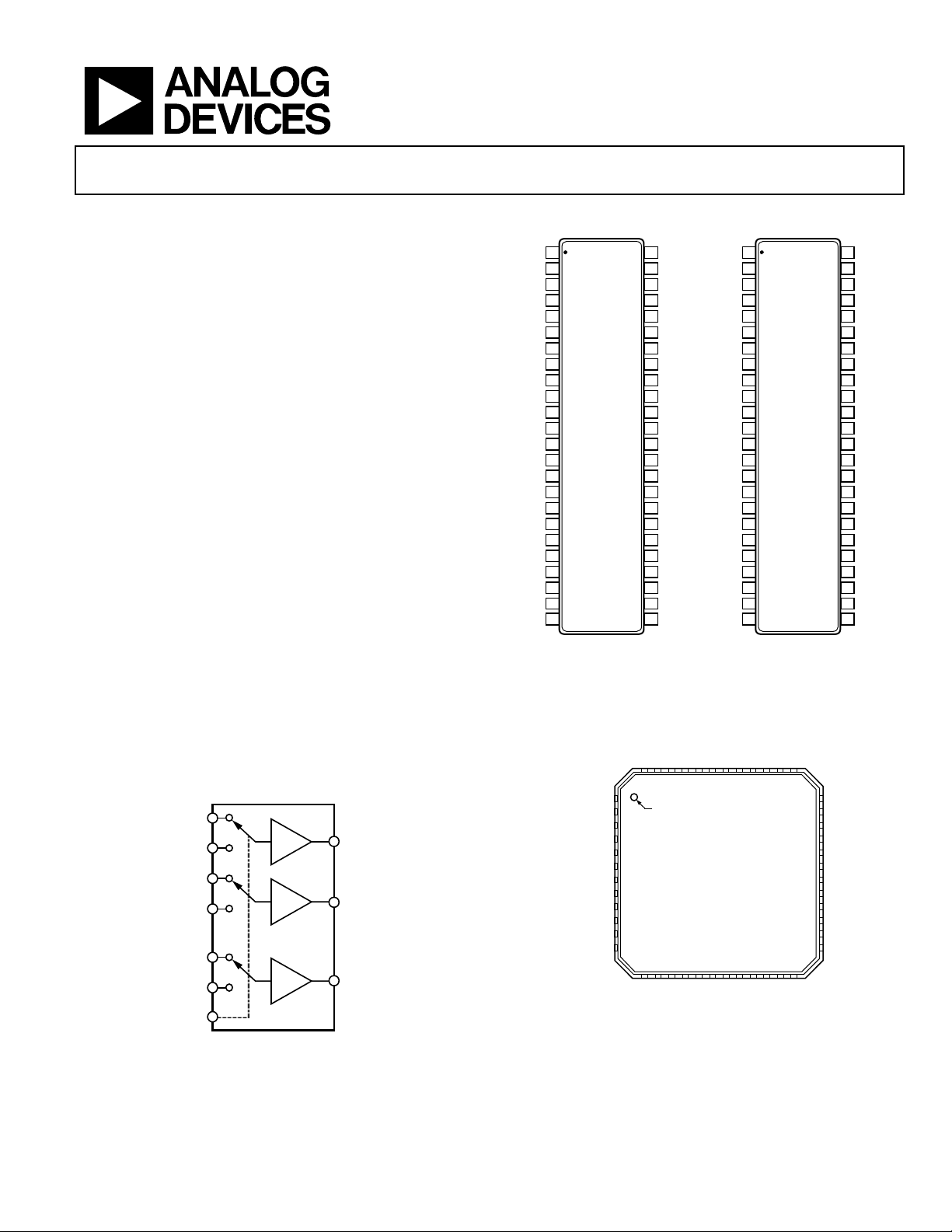
The AD8509 and AD8511 are 9-channel and 11-channel LCD
reference buffers, respectively, designed to drive 64 gray scale
column drivers. Each buffer has an A/B input to select between
two voltages for LCD displays. These buffers drive the resistor
ladders of LCD column drivers for gamma correction. The LCD
drivers have higher slew rates and higher output drive currents
than similar competitive parts. This increases the stability of
the reference ladder, resulting in better gray scale and visual
performance.
The AD8509 and AD8511 are specified over the −40°C to +85°C
temperature range. They are available in 48-lead, Pb-free TSSOP
packages in tape and reel. Additionally, the ADD8511 is available
in a 48-lead, Pb-free LFCSP package.
INA1
INB1
INA2
INB2
INA3
INB3
INA4
INB4
INA5
INB5
INA6
INB6
INA7
INB7
INA8
INB8
INA9
INB9
NC
NC
NC
NC
NC
NC
1
2
3
4
5
6
7
8
9
10
11
12
13
14
15
16
17
18
19
20
21
22
23
24
48
NC
47
NC
46
NC
45
NC
44
V
CC
GND
43
VO1
42
VO2
AD8509
TOP VIEW
(Not to Scale)
NC = NO CO NNECT
41
VO3
40
VO4
39
V
38
CC
GND
37
VO5
36
VO6
35
VO7
34
VO8
33
VO9
32
GND
31
30
V
CC
29
A/B
NC
28
NC
27
26
NC
NC
25
Figure 2. AD8509 and AD8511 48-Lead TSSOP (RV Suffix)
NCNCINB2
INA2
4847464544434241403938
INB1
NC
INA1
INB1
INA2
INB2
INA3
INB3
INA4
INB4
INA5
INB5
INA6
INB6
INA7
INB7
INA8
INB8
INA9
INB9
INA10
INB10
NC
INA11
INB11
INA1NCVO1
1
2
3
4
5
6
7
8
AD8511
9
TOP VIEW
(Not to Scale)
10
11
12
13
14
15
16
17
18
19
20
21
22
23
24
NC = NO CO NNECT
CC
GNDNCNC
V
48
NC
47
VO1
46
NC
45
NC
44
V
CC
GND
43
VO2
42
VO3
41
VO4
40
VO5
39
V
38
CC
GND
37
VO6
36
VO7
35
VO8
34
VO9
33
VO10
32
GND
31
30
V
CC
29
A/B
NC
28
NC
27
26
VO11
NC
25
03237-012
37
FUNCTIONAL BLOCK DIAGRAM
INA1
INB1
INA2
INB2
INA11
INB11
A/B
Figure 1.
Rev. C
Information furnished by Analog Devices is believed to be accurate and reliable. However, no
responsibility is assumed by Anal og Devices for its use, nor for any infringements of patents or ot her
rights of third parties that may result from its use. Specifications subject to change without notice. No
license is granted by implication or otherwise under any patent or patent rights of Analog Devices.
Trademarks and registered trademarks are the property of their respective owners.
VO1
VO2
VO11
03237-001
INA3
1
INB3
2
INA4
3
INB4
4
INA5
5
INB5
6
INA6
7
INB6
8
INA7
9
INB7
10
INA8
11
INB8
12
NC = NO CONNECT
PIN 1
INDICATOR
AD8511
TOP VIEW
(Not to Scale)
13141516171819
INA9
INB9
INA11NCINB11
INA10
INB10
2021222324
NC
NC
A/B
VO11
CC
V
Figure 3. AD8511 48-Lead LFCSP
One Technology Way, P.O. Box 9106, Norwood, MA 02062-9106, U.S.A.
Tel: 781.329.4700 www.analog.com
Fax: 781.461.3113 ©2006 Analog Devices, Inc. All rights reserved.
VO236
VO3
35
VO4
34
VO5
33
V
32
CC
GND
31
VO6
30
VO7
29
VO8
28
VO9
27
VO10
26
GND
25
03237-011
Page 2

AD8509/AD8511
TABLE OF CONTENTS
Features.............................................................................................. 1
Application ........................................................................................ 1
General Description ......................................................................... 1
Functional Block Diagram .............................................................. 1
Pin Configurations ........................................................................... 1
Revision History ............................................................................... 2
Specifications..................................................................................... 3
Electrical Characteristics ............................................................. 3
REVISION HISTORY
2/06—Rev. C
Added LFCSP Package.......................................................Universal
Added Pin Configurations and Function Descriptions Section... 5
Updated Outline Dimensions ........................................................ 9
Changes to Ordering Guide............................................................ 9
1/05—Rev. A to Rev. B
Changed Maximum Operating Voltage...........................Universal
Change to Features List.................................................................... 1
Changes to Specifications Table...................................................... 3
Changes to Ordering Guide............................................................ 8
Absolute Maximum Ratings ............................................................4
Thermal Resistance.......................................................................4
ESD Caution...................................................................................4
Pin Configurations and Function Descriptions............................5
Typical Performance Characteristics..............................................6
Applications........................................................................................8
Outline Dimensions..........................................................................9
Ordering Guide .............................................................................9
9/04—Rev. 0 to Rev. A
Format Updated.................................................................. Universal
Added Pb-Free Part............................................................Universal
Changed Temperature Range............................................Universal
Changed Applications Section.........................................................1
Changes to Ordering Guide.............................................................8
10/97—Revision 0: Initial Version
Rev. C | Page 2 of 12
Page 3

AD8509/AD8511
SPECIFICATIONS
ELECTRICAL CHARACTERISTICS
VS = 5 V, TA = 25°C, unless otherwise noted.
Table 1.
Parameter Symbol Conditions Min Typ Max Unit
INPUT CHARACTERISTICS
Offset Voltage VOS 20 mV
Input Bias Current IB 50 nA
Voltage Gain AVO 0.985 V/V
OUTPUT CHARACTERISTICS
Output Voltage High VOH I
Output Voltage Low VOL I
Output Short-Circuit Current ISC 120 350 mA
POWER SUPPLY
Load Regulation VIN = 0.5 V to 4.5 V, I
V
Supply Current ISY AD8509, VIN = 2.5 V 8.5 mA
I
AD8511, VIN = 2.5 V 10 mA
SY
Supply Voltage Range VS 3.3 6.5 V
DYNAMIC PERFORMANCE
Slew Rate CL = 15 pF 7 V/μs
R
Settling Time tS IDC = 13 mA (sink/source) 3 6 μs
LOGIC INPUT CHARACTERISTICS
Input Current Low IIL 1.0 μA
Input Current High IIH 1.5 μA
Input Voltage Low VIL 0.8 V
Input Voltage High VIH 2.0 V
= +20 mA 4.8 V
LOAD
= −20 mA 200 mV
LOAD
= 20 mA 7 mV
SOURCE
= 0.5 V to 4.5 V, I
IN
= 250 Ω 6.2 V/μs
L
= 20 mA 7 mV
SINK
Rev. C | Page 3 of 12
Page 4
AD8509/AD8511
ABSOLUTE MAXIMUM RATINGS
Table 2.
Parameter Rating
Supply Voltage 7 V
Input Voltage GND to VS
Storage Temperature Range
TSSOP (RV-48)
Operating Temperature Range
Junction Temperature Range
TSSOP (RV-48) Package
Lead Temperature Range
(Soldering, 60 sec) 300°C
Stresses above those listed under Absolute Maximum Ratings
may cause permanent damage to the device. This is a stress
rating only; functional operation of the device at these or any
other conditions above those indicated in the operational
section of this specification is not implied. Exposure to absolute
maximum rating conditions for extended periods may affect
device reliability.
−65°C to +150°C
−40°C to +85°C
−65°C to +150°C
THERMAL RESISTANCE
θJA is specified for the worst-case conditions, that is, a device
soldered in a circuit board for surface-mount packages.
Table 3. Thermal Resistance
Package Type θJA θJC Unit
48-Lead, Pb-Free SSOP (RV-48) 115 42 °C/W
48-Lead, Pb-Free LFCSP (CP-48-1) 125 29 °C/W
Table 4. MUX Function
A/B Select Input
Logic High INAx
Logic Low INBx
ESD CAUTION
ESD (electrostatic discharge) sensitive device. Electrostatic charges as high as 4000 V readily accumulate on
the human body and test equipment and can discharge without detection. Although this product features
proprietary ESD protection circuitry, permanent damage may occur on devices subjected to high energy
electrostatic discharges. Therefore, proper ESD precautions are recommended to avoid performance
degradation or loss of functionality.
Rev. C | Page 4 of 12
Page 5

AD8509/AD8511
PIN CONFIGURATIONS AND FUNCTION DESCRIPTIONS
1
NC
2
NC
3
NC
4
INA1
5
INB1
6
INA2
7
INB2
8
INA3
INB3
INA4
INB4
INA5
INB5
INA6
INB6
INA7
INB7
INA8
INB8
INA9
INB9
NC
NC
NC
9
(Not to Scale)
10
11
12
13
14
15
16
17
18
19
20
21
22
23
24
AD8509
TOP VIEW
NC = NO CO NNECT
Figure 4. AD8509
48-Lead TSSOP (RV Suffix)
48
NC
47
NC
46
NC
45
NC
44
V
CC
43
GND
42
VO1
41
VO2
40
VO3
39
VO4
38
V
CC
37
GND
36
VO5
35
VO6
34
VO7
33
VO8
32
VO9
31
GND
30
V
CC
29
A/B
NC
28
NC
27
26
NC
NC
25
03237-002
NC
INA1
INB1
INA2
INB2
INA3
INB3
INA4
INB4
INA5
INB5
INA6
INB6
INA7
INB7
INA8
INB8
INA9
INB9
INA10
INB10
NC
INA11
INB11
1
2
3
4
5
6
7
8
AD8511
9
TOP VIEW
(Not to Scale)
10
11
12
13
14
15
16
17
18
19
20
21
22
23
24
NC = NO CO NNECT
48
NC
47
VO1
46
NC
45
NC
44
V
CC
43
GND
42
VO2
41
VO3
40
VO4
39
VO5
38
V
CC
37
GND
36
VO6
35
VO7
34
VO8
33
VO9
32
VO10
31
GND
30
V
CC
29
A/B
NC
28
NC
27
26
VO11
NC
25
03237-010
Figure 5. AD8511
48-Lead TSSOP (RV Suffix)
CC
GNDNCNC
V
2021222324
NC
NC
A/B
VO11
37
VO236
VO3
35
VO4
34
VO5
33
V
32
CC
31
GND
30
VO6
29
VO7
28
VO8
27
VO9
26
VO10
25
GND
CC
V
03237-011
INA3
1
INB3
2
INA4
3
INB4
4
INA5
5
INB5
6
INA6
7
INB6
8
INA7
9
INB7
10
INA8
11
INB8
12
NC = NO CONNECT
NCNCINB2
INA2
INB1
INA1NCVO1
4847464544434241403938
PIN 1
INDICATOR
AD8511
TOP VIEW
(Not to Scale)
13141516171819
INA9
INB9
INA11NCINB11
INA10
INB10
Figure 6. AD8511 (48-Lead LFCSP)
Table 5. Pin Function Descriptions
Pin No.
AD8509 (TSSOP) AD8511 (TSSOP) AD8511 (LFCSP) Mnemonic Description
4, 6, 8, 10, 12, 14, 16, 18, 20 2, 4, 6, 8, 10, 12, 14, 16, 18, 20, 23 1, 3, 5, 7, 9, 11, 13, 15, 17, 43, 45 INAx MUX Input
5, 7, 9, 11, 13, 15, 17, 19, 21 3, 5, 7, 9, 11, 13, 15, 17, 19, 21, 24 2, 4, 6, 8, 10, 12, 14, 16, 19, 44, 46 INBx MUX Input
32 to 36, 39 to 42 26, 32 to 36, 39 to 42, 47 20, 26 to 30, 33 to 36, 41 VOx MUX Output
29 29 22 A/B Input Selection Pin
30, 38, 44 30, 38, 44 24, 32, 40 Vcc Bias
31, 37, 43 31, 37, 43 25, 31, 39 GND Ground
1 to 3, 22 to 28, 45 to 48 1, 22, 25 27, 28, 45, 46, 48 18, 21, 23, 37, 38, 42, 47, 48 NC No Connection
Rev. C | Page 5 of 12
Page 6

AD8509/AD8511
TYPICAL PERFORMANCE CHARACTERISTICS
10
9
VS=5V
=NOLOAD
R
L
1k
VS=5V
=25°C
T
A
8
7
6
5
SUPPLY CURRENT (mA)
4
3
–35 –15 5 25 45 65 85 105
TEMPERATURE (°C)
Figure 7. Supply Current vs. Temperature Figure 9. Output Voltage to Supply Rail vs. Load Current
10
9
8
7
6
5
4
3
SUPPLY CURRENT (mA)
2
1
0
054321
AD8509
COMMON-MO DE VOLTAGE (V)
AD8511
VS=5V
T
=25°C
A
R
=NOLOAD
L
Figure 8. Supply Current vs. Common-Mode Voltage
100
10
Δ OUTPUT VOLTAGE (mV)
03237-003
1
0.1 100101
LOAD CURRENT (mA)
SOURCE
SINK
VS=5V
T
= 25°C
A
R
=NOLOAD
L
C
=15pF
L
03237-004
620mV 2.5V
Figure 10. Large Signal Transient Response—Rising
03237-006
03237-005
Rev. C | Page 6 of 12
Page 7

AD8509/AD8511
VS=5V
T
=25°C
A
R
=NOLOAD
L
C
= 15pF
L
VS=5V
T
= 25°C
A
R
= 250Ω
L
C
= 15pF
L
620mV 2.5V
03237-007
620mV 2.5V
03237-009
Figure 11. Large Signal Transient Response—Falling
VS=5V
T
=25°C
A
R
= 250Ω
L
C
= 15pF
L
620mV 2.5V
Figure 12. Large Signal Transient Response—Rising
03237-008
Figure 13. Large Signal Transient Response—Falling
Rev. C | Page 7 of 12
Page 8

AD8509/AD8511
APPLICATIONS
The AD8509 and AD8511 are CMOS buffers with A/B inputs
that are used to select between two different reference voltages set
up by an external resistor ladder. Input bias currents are orders
of magnitude less than competitive parts. This allows very large
resistor ladders to be used to save supply current. A guaranteed
value of 50 nA is much higher than actual values and is limited
by leakage in the test system.
Buffer outputs are designed to drive resistive loads. They are
also stable with capacitive loads, so no resistors should be used
in series with these outputs to attain the best display performance. Outputs have high slew rates and 6 μs settling times. Each
output can deliver a minimum of 120 mA, assuring fast response
to varying loads.
The AD8509 is a 9-channel buffer and is similar to the LMC6009
in functionality. The AD8511 is an 11-channel buffer similar to
the CL-FP6131. However, the control to select either 9- or
11-channel operation, the EN_11 pin of the CL-FP6131, is not
available on the AD8511. If 9-channel operation is desired, use
the AD8509.
Power supply pins on the AD8509 and AD8511 have multiple
ground and V
connections. Because of the high peak currents
CC
that these buffers can deliver, it is strongly recommended to
connect all of the ground and V
the V
pins.
CC
pins, and suitably bypass
CC
Rev. C | Page 8 of 12
Page 9

AD8509/AD8511
OUTLINE DIMENSIONS
12.60
12.50
12.40
1.20 MAX
SEATING
PLANE
25
6.20
6.10
6.00
8.10 BSC
24
0.75
0.60
0.45
0.20
0.09
8°
0°
0.15
0.05
PIN 1
48
1
0.50
BSC
0.27
0.17
COMPLIANT TO JEDEC STANDARDS MO-153-ED
Figure 14. 48-Lead Thin Shrink Small Outline Package [TSSOP]
(RV-48)
Dimensions shown in millimeters
PAD
0.30
0.23
0.18
PIN 1
48
INDICATOR
1
5.25
5.10 SQ
4.95
BSC SQ
PIN 1
INDICATOR
7.00
TOP
VIEW
6.75
BSC SQ
0.60 MAX
0.60 MAX
37
36
(BOTTOM VIEW)
EXPOSED
1.00
0.85
0.80
12° MAX
SEATING
PLANE
0.50
0.40
0.30
0.80 MAX
0.65 TYP
0.50 BSC
COMPLIANT TO JEDEC STANDARDS MO-220-VKKD-2
0.05 MAX
0.02 NOM
0.20 REF
25
24
COPLANARITY
0.08
5.50
REF
12
13
0.25 MIN
Figure 15. 48-Lead Lead Frame Chip Scale Package [LFCSP_VQ]
7 mm x 7 mm Body, Very Thin Quad
(CP-48-1)
Dimensions shown in millimeters
ORDERING GUIDE
1
Model Temperature Range Package Description Package Option
AD8509ARU-REEL −40°C to +85°C 48-Lead Thin Shrink Small Outline Package [TSSOP] RV-48
AD8509ARUZ-REEL −40°C to +85°C 48-Lead Thin Shrink Small Outline Package [TSSOP] RV-48
AD8511ARU-REEL −40°C to +85°C 48-Lead Thin Shrink Small Outline Package [TSSOP] RV-48
AD8511ARUZ-REEL −40°C to +85°C 48-Lead Thin Shrink Small Outline Package [TSSOP] RV-48
AD8511ACPZ-REEL −40°C to +85°C 48-Lead Lead Frame Chip Scale Package [LFCSP_VQ] CP-48-1
1
All models only available in 2,500-piece reels.
2
Z = Pb-free part.
2
2
2
Rev. C | Page 9 of 12
Page 10

AD8509/AD8511
NOTES
Rev. C | Page 10 of 12
Page 11

AD8509/AD8511
NOTES
Rev. C | Page 11 of 12
Page 12

AD8509/AD8511
NOTES
©2006 Analog Devices, Inc. All rights reserved. Trademarks and
registered trademarks are the property of their respective owners.
C03237-0-2/06(C)
Rev. C | Page 12 of 12
 Loading...