

Page 1
REV. B
Information furnished by Analog Devices is believed to be accurate and
reliable. However, no responsibility is assumed by Analog Devices for its
use, nor for any infringements of patents or other rights of third parties
which may result from its use. No license is granted by implication or
otherwise under any patent or patent rights of Analog Devices.
a
AD848/AD849
One Technology Way, P.O. Box 9106, Norwood, MA 02062-9106, U.S.A.
Tel: 617/329-4700 Fax: 617/326-8703
High Speed, Low Power
Monolithic Op Amp
FEATURES
725 MHz Gain Bandwidth – AD849
175 MHz Gain Bandwidth – AD848
4.8 mA Supply Current
300 V/ms Slew Rate
80 ns Settling Time to 0.1% for a 10 V Step – AD849
Differential Gain: AD848 = 0.07%, AD849 = 0.08%
Differential Phase: AD848 = 0.088, AD849 = 0.048
Drives Capacitive Loads
DC PERFORMANCE
3 nV/√Hz Input Voltage Noise – AD849
85 V/mV Open Loop Gain into a 1 kV Load – AD849
1 mV max Input Offset Voltage
Performance Specified for 65 V and 615 V Operation
Available in Plastic, Hermetic Cerdip and Small Outline
Packages. Chips and MIL-STD-883B Parts Available.
Available in Tape and Reel in Accordance with
EIA-481A Standard
APPLICATIONS
Cable Drivers
8- and 10-Bit Data Acquisition Systems
Video and R
F
Amplification
Signal Generators
PRODUCT DESCRIPTION
The AD848 and AD849 are high speed, low power monolithic
operational amplifiers. The AD848 is internally compensated so
that it is stable for closed loop gains of 5 or greater. The AD849
is fully decompensated and is stable at gains greater than 24.
The AD848 and AD849 achieve their combination of fast ac
and good dc performance by utilizing Analog Devices’ junction
isolated complementary bipolar (CB) process. This process
enables these op amps to achieve their high speed while only
requiring 4.8 mA of current from the power supplies.
The AD848 and AD849 are members of Analog Devices’ family
of high speed op amps. This family includes, among others, the
AD847 which is unity gain stable, with a gain bandwidth of
50 MHz. For more demanding applications, the AD840,
AD841 and AD842 offer even greater precision and greater
output current drive.
The AD848 and AD849 have good dc performance. When
operating with ±5 V supplies, they offer open loop gains of
13 V/mV (AD848 with a 500 Ω load) and low input offset
voltage of 1 mV maximum. Common-mode rejection is a
minimum of 92 dB. Output voltage swing is ± 3 V even into
loads as low as 150 Ω.
APPLICATIONS HIGHLIGHTS
1. The high slew rate and fast settling time of the AD848 and
AD849 make them ideal for video instrumentation circuitry,
low noise pre-amps and line drivers.
2. In order to meet the needs of both video and data acquisition
applications, the AD848 and AD849 are optimized and
tested for ±5 V and ±15 V power supply operation.
3. Both amplifiers offer full power bandwidth greater than
20 MHz (for 2 V p-p with ± 5 V supplies).
4. The AD848 and AD849 remain stable when driving any
capacitive load.
5. Laser wafer trimming reduces the input offset voltage to
1 mV maximum on all grades, thus eliminating the need for
external offset nulling in many applications.
6. The AD848 is an enhanced replacement for the LM6164
series and can function as a pin-for-pin replacement for
many high speed amplifiers such as the HA2520/2/5 and
EL2020 in applications where the gain is 5 or greater.
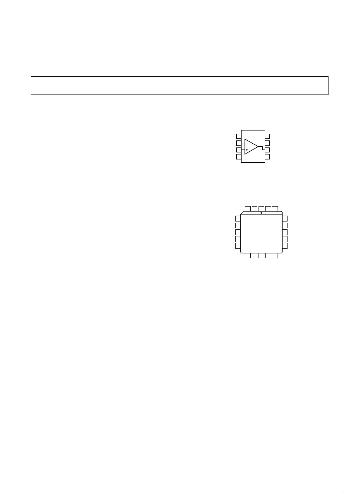
CONNECTION DIAGRAMS
Plastic (N),
Small Outline (R) and
Cerdip (Q) Packages
1
2
3
4
8
7
6
5TOP VIEW
(Not to Scale)
NC = NO CONNECT
NULL
NC
OUTPUT
+V
S
NULL
–IN
+IN
–V
S
AD848/49
20-Terminal LCC Pinout
NC = NO CONNECT
NC
NC
NC
OFFSET
NULL
NC
V+
NC
NC
NC
–IN
NC
NC
+IN
NC
NC
NC
NC
V–
1418 1617 15
19
20
3
1
2
78465
13
12
9
11
10
TOP VIEW
(Not to Scale)
AD848SE/883B
OFFSET
NULL
OUTPUT
Page 2
REV. B
–2–
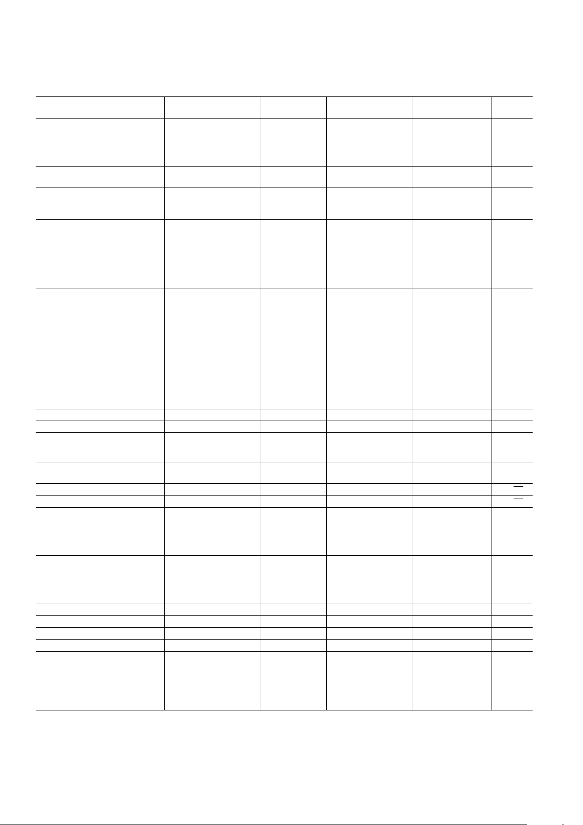
AD848/AD849–SPECIFICA TIONS
AD848J AD848A/S
Model Conditions V
S
Min Typ Max Min Typ Max Units
INPUT OFFSET VOLTAGE
1
±5 V 0.2 1 0.2 1 mV
±15 V 0.5 2.3 0.5 2.3 mV
T
MIN
to T
MAX
±5 V 1.5 2 mV
±15 V 3.0 3.5 mV
Offset Drift ± 5 V, ±15 V 7 7 µV/°C
INPUT BIAS CURRENT ± 5 V, ±15 V 3.3 6.6 3.3 6.6/5 µA
T
MIN
to T
MAX
± 5 V, ±15 V 7.2 7.5 µA
INPUT OFFSET CURRENT ± 5 V, ±15 V 50 300 50 300 nA
T
MIN
to T
MAX
± 5 V, ±15 V 400 400 nA
Offset Current Drift ± 5 V, ±15 V 0.3 0.3 nA/°C
OPEN LOOP GAIN V
O
= ±2.5 V ±5V
R
LOAD
= 500 Ω 9 13 9 13 V/mV
T
MIN
to T
MAX
7 7/5 V/mV
R
LOAD
= 150 Ω 8 8 V/mV
V
OUT
= ±10 V ±15 V
R
LOAD
= 1 kΩ 12 20 12 20 V/mV
T
MIN
to T
MAX
8 8/6 V/mV
DYNAMIC PERFORMANCE
Gain Bandwidth A
VCL
≥ 5 ±5 V 125 125 MHz
±15 V 175 175 MHz
Full Power Bandwidth
2
VO = 2 V p-p,
R
L
= 500 Ω±5 V 24 24 MHz
V
O
= 20 V p-p,
R
L
= 1 kΩ±15 V 4.7 4.7 MHz
Slew Rate ±5 V 200 200 V/µs
R
LOAD
= 1 kΩ±15 V 225 300 225 300 V/µs
Settling Time to 0.1% –2.5 V to +2.5 V ±5 V 65 65 ns
10 V Step, A
V
= –4 ±15 V 100 100 ns
Phase Margin C
LOAD
= 10 pF ±15 V
R
LOAD
= 1 kΩ 60 60 Degrees
DIFFERENTIAL GAIN f = 4.4 MHz ±15 V 0.07 0.07 %
DIFFERENTIAL PHASE f = 4.4 MHz ±15 V 0.08 0.08 Degree
COMMON-MODE REJECTION V
CM
= ±2.5 V ±5 V 92 105 92 105 dB
V
CM
= ±12 V ±15 V 92 105 92 105 dB
T
MIN
to T
MAX
88 88 dB
POWER SUPPLY REJECTION V
S
= ± 4.5 V to ±18 V 85 98 85 98 dB
T
MIN
to T
MAX
80 80 dB
INPUT VOLTAGE NOISE f = 10 kHz ±15 V 5 5 nV/√Hz
INPUT CURRENT NOISE f = 10 kHz ±15 V 1.5 1.5 pA/√Hz
INPUT COMMON-MODE
VOLTAGE RANGE ± 5 V +4.3 +4.3 V
–3.4 –3.4 V
± 15 V +14.3 +14.3 V
–13.4 –13.4 V
OUTPUT VOLTAGE SWING R
LOAD
= 500 Ω±5 V 3.0 3.6 3.0 3.6 ±V
R
LOAD
= 150 Ω±5V 2.5 3 2.5 3 ±V
R
LOAD
= 50 Ω±5 V 1.4 1.4 ±V
R
LOAD
= 1 kΩ±15 V 12 12 ±V
R
LOAD
= 500 Ω±15 V 10 10 ±V
SHORT CIRCUIT CURRENT ± 15 V 32 32 mA
INPUT RESISTANCE 70 70 kΩ
INPUT CAPACITANCE 1.5 1.5 pF
OUTPUT RESISTANCE Open Loop 15 15 Ω
POWER SUPPLY
Operating Range 64.5 618 64.5 618 V
Quiescent Current ± 5 V 4.8 6.0 4.8 6.0 mA
T
MIN
to T
MAX
7.4 7.4/8.3 mA
±15 V 5.1 6.8 5.1 6.8 mA
T
MIN
to T
MAX
8.0 8.0/9.0 mA
NOTES
1
Input offset voltage specifications are guaranteed after 5 minutes at TA = +25°C.
2
Full power bandwidth = slew rate/2 π V
PEAK
. Refer to Figure 1.
All min and max specifications are guaranteed. Specifications in boldface are tested on all production units at final electrical test. All others are guaranteed but not necessarily tested.
Specifications subject to change without notice.
(@ TA = +258C, unless otherwise noted)
Page 3
REV. B
–3–
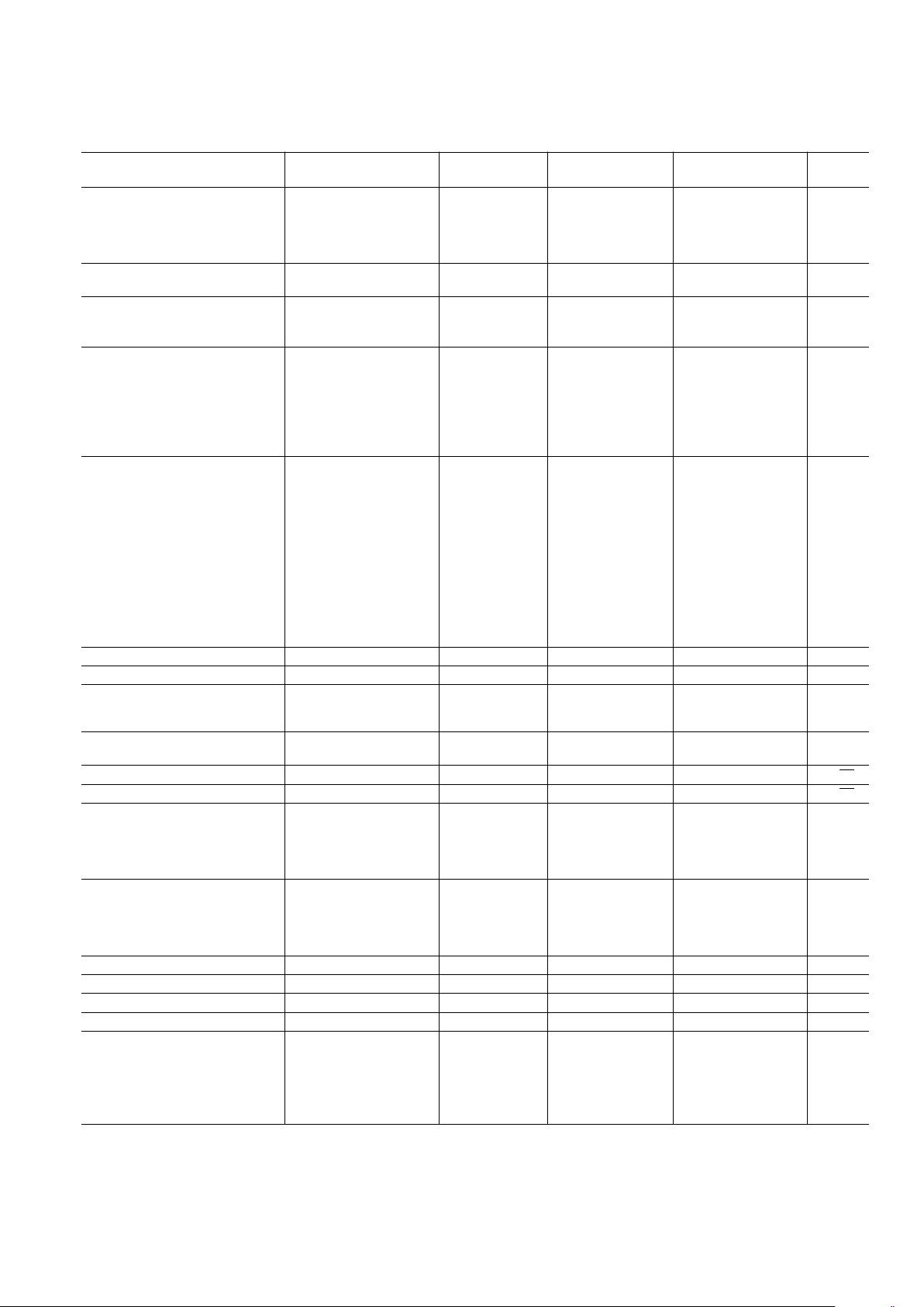
AD849J AD849A/S
Model Conditions V
S
Min Typ Max Min Typ Max Units
INPUT OFFSET VOLTAGE
1
±5 V 0.3 1 0.1 0.75 mV
±15 V 0.3 1 0.1 0.75 mV
T
MIN
to T
MAX
±5 V 1.3 1.0 mV
±15 V 1.3 1.0 mV
Offset Drift ±5 V, ±15 V 2 2 µV/°C
INPUT BIAS CURRENT ±5 V, ± 15 V 3.3 6.6 3.3 6.6/5 µA
T
MIN
to T
MAX
±5 V, ± 15 V 7.2 7.5 µA
INPUT OFFSET CURRENT ±5 V, ± 15 V 50 300 50 300 nA
T
MIN
to T
MAX
±5 V, ± 15 V 400 400 nA
Offset Current Drift ±5 V, ± 15 V 0.3 0.3 nA/°C
OPEN LOOP GAIN V
O
= ±2.5 V ±5V
R
LOAD
= 500 Ω 30 50 30 50 V/mV
T
MIN
to T
MAX
20 20/15 V/mV
R
LOAD
= 150 Ω 32 32 V/mV
V
OUT
= ±10 V ±15 V
R
LOAD
= 1 kΩ 45 85 45 85 V/mV
T
MIN
to T
MAX
30 30/25 V/mV
DYNAMIC PERFORMANCE
Gain Bandwidth A
VCL
≥ 25 ±5 V 520 520 MHz
±15 V 725 725 MHz
Full Power Bandwidth
2
VO = 2 V p-p,
R
L
= 500 Ω±5 V 20 20 MHz
V
O
= 20 V p-p,
R
L
= 1 kΩ±15 V 4.7 4.7 MHz
Slew Rate ±5 V 200 200 V/µs
R
LOAD
= 1 kΩ±15 V 225 300 225 300 V/µs
Settling Time to 0.1% –2.5 V to +2.5 V ±5 V 65 65 ns
10 V Step, A
V
= –24 ±15 V 80 80 ns
Phase Margin C
LOAD
= 10 pF ±15 V
R
LOAD
= 1 kΩ 60 60 Degrees
DIFFERENTIAL GAIN f = 4.4 MHz ±15 V 0.08 0.08 %
DIFFERENTIAL PHASE f = 4.4 MHz ±15 V 0.04 0.04 Degrees
COMMON-MODE REJECTION V
CM
= ±2.5 V ±5 V 100 115 100 115 dB
V
CM
= ±12 V ±15 V 100 115 100 115 dB
T
MIN
to T
MAX
96 96 dB
POWER SUPPLY REJECTION V
S
= ±4.5 V to ±18 V 98 120 98 120 dB
T
MIN
to T
MAX
94 94 dB
INPUT VOLTAGE NOISE f = 10 kHz ±15 V 3 3 nV/√Hz
INPUT CURRENT NOISE f = 10 kHz ±15 V 1.5 1.5 pA/√Hz
INPUT COMMON-MODE
VOLTAGE RANGE ± 5 V +4.3 +4.3 V
–3.4 –3.4 V
± 15 V +14.3 +14.3 V
–13.4 –13.4 V
OUTPUT VOLTAGE SWING R
LOAD
= 500 Ω±5 V 3.0 3.6 3.0 3.6 ±V
R
LOAD
= 150 Ω±5V 2.5 3 2.5 3 ±V
R
LOAD
= 50 Ω±5 V 1.4 1.4 ±V
R
LOAD
= 1 kΩ±15 V 12 12 ± V
R
LOAD
= 500 Ω±15 V 10 10 ±V
SHORT CIRCUIT CURRENT ±15 V 32 32 mA
INPUT RESISTANCE 25 25 kΩ
INPUT CAPACITANCE 1.5 1.5 pF
OUTPUT RESISTANCE Open Loop 15 15 Ω
POWER SUPPLY
Operating Range 64.5 618 64.5 618 V
Quiescent Current ±5 V 4.8 6.0 4.8 6.0 mA
T
MIN
to T
MAX
7.4 7.4/8.3 mA
±15 V 5.1 6.8 5.1 6.8 mA
T
MIN
to T
MAX
8.0 8.0/9.0 mA
NOTES
1
Input offset voltage specifications are guaranteed after 5 minutes at TA = +25°C.
2
Full power bandwidth = slew rate/2 π V
PEAK
. Refer to Figure 1.
All min and max specifications are guaranteed. Specifications in boldface are tested on all production units at final electrical test. All others are guaranteed but not necessarily tested.
Specifications subject to change without notice.
AD848/AD849
Page 4

AD848/AD849
REV. B
–4–
ABSOLUTE MAXIMUM RATINGS
1
Supply Voltage . . . . . . . . . . . . . . . . . . . . . . . . . . . . . . . ±18 V
Internal Power Dissipation
2
Plastic (N) . . . . . . . . . . . . . . . . . . . . . . . . . . . . . . 1.1 Watts
Small Outline (R) . . . . . . . . . . . . . . . . . . . . . . . . . 0.9 Watts
Cerdip (Q) . . . . . . . . . . . . . . . . . . . . . . . . . . . . . . 1.1 Watts
LCC (E) . . . . . . . . . . . . . . . . . . . . . . . . . . . . . . . . 0.8 Watts
Input Voltage . . . . . . . . . . . . . . . . . . . . . . . . . . . . . . . . . . ±V
S
Differential Input Voltage . . . . . . . . . . . . . . . . . . . . . . . ±6 V
Storage Temperature Range (Q) . . . . . . . . –65°C to +150°C
(N, R) . . . . . . . . . . . . . . . . . . . . . . . . . . –65°C to +125°C
Junction Temperature . . . . . . . . . . . . . . . . . . . . . . . . +175°C
Lead Temperature Range (Soldering 60 sec) . . . . . . . +300°C
NOTES
1
Stresses above those listed under “Absolute Maximum Ratings” may cause permanent damage to the device. This is a stress rating only, and functional operation of the device at these or any other conditions above those indicated in the
operational section of this specification is not implied. Exposure to absolute
maximum rating conditions for extended periods may affect device reliability.
2
LCC: θJA = 150°C/Watt
Mini-DIP Package: θJA = 110°C/Watt
Cerdip Package: θJA = 110°C/Watt
Small Outline Package: θJA = 155°C/Watt.
METALIZATION PHOTOGRAPH
Contact factory for latest dimensions. (AD848 and AD849 are identical
except for the part number in the upper right.)
Dimensions shown in inches and (mm).
ORDERING GUIDE
Gain Min Max
Bandwidth Stable Offset Voltage Temperature Package
Model MHz Gain mV Range – 8C Option
1
AD848JN 175 5 1 0 to +70 N-8
AD848JR
2
175 5 1 0 to +70 R-8
AD848JCHIPS 175 5 1 0 to +70 Die Form
AD848AQ 175 5 1 –40 to +85 Q-8
AD848SQ 175 5 1 –55 to +125 Q-8
AD848SQ/883B 175 5 1 –55 to +125 Q-8
AD848SE/883B 175 5 1 –55 to +125 E-20A
AD849JN 725 25 1 0 to +70 N-8
AD849JR
2
725 25 1 0 to +70 R-8
AD849AQ 725 25 0.75 –40 to +85 Q-8
AD849SQ 725 25 0.75 –55 to +125 Q-8
AD849SQ/883B 725 25 0.75 –55 to +125 Q-8
AD847J/A/S 50 1 1 See AD847 Data Sheet
NOTES
1
E = LCC; N = Plastic DIP; Q = Cerdip; R = Small Outline IC (SOIC).
2
Plastic SOIC (R) available in tape and reel. AD848 available in S grade chips. AD849 available in J and S grade
chips.
Page 5

AD848/AD849
REV. B
–5–
Figure 1. AD848 Inverting Amplifier Configuration
Figure 1a. AD848 Large Signal Pulse Response
Figure 1b. AD848 Small Signal Pulse Response
OFFSET NULLING
The input voltage of the AD848 and AD849 are very low for
high speed op amps, but if additional nulling is required, the
circuit shown in Figure 3 can be used.
For high performance circuits it is recommended that a resistor
(R
B
in Figures 1 and 2) be used to reduce bias current errors by
matching the impedance at each input. The offset voltage error
caused by the input currents is decreased by more than an order
of magnitude.
Figure 2. AD849 Inverting Amplifier Configuration
Figure 2a. AD849 Large Signal Pulse Response
Figure 2b. AD849 Small Signal Pulse Response
Figure 3. Offset Nulling
Page 6

Figure 4. Quiescent Current vs.
Supply Voltage (AD848 and AD849)
Figure 7. Open Loop Gain vs.
Load Resistance (AD848)
Figure 10. Quiescent Current vs.
Temperature (AD848 and AD849)
AD848/AD849–Typical Characteristics
REV. B–6–
(@ TA = +258C and VS = 615 V, unless otherwise noted)
Figure 5. Large Signal Frequency
Response (AD848 and AD849)
Figure 8. Open Loop Gain vs.
Load Resistance (AD849)
Figure 11. Short Circuit Current
Limit vs. Temperature (AD848
and AD849)
Figure 6. Output Voltage Swing vs.
Load Resistance (AD848 and AD849)
Figure 9. Output Swing and
Error vs. Settling Time (AD848)
Figure 12. Input Bias Current vs.
Temperature (AD848 and AD849)
Page 7

AD848/AD849
REV. B
–7–
Figure 13. Open Loop Gain and
Phase Margin vs. Frequency (AD848)
Figure 16. Harmonic Distortion vs.
Frequency (AD848)
Figure 19. Power Supply Rejection vs.
Frequency (AD848)
Figure 14. Open Loop Gain and
Phase Margin vs. Frequency (AD849)
Figure 17. Harmonic Distortion vs.
Frequency (AD849)
Figure 20. Power Supply Rejection vs.
Frequency (AD849)
Figure 15. Normalized Gain Bandwidth Product vs. Temperature
(AD848 and AD849)
Figure 18. Slew Rate vs. Temperature
(AD848 and AD849)
Figure 21. Common-Mode
Rejection vs. Frequency
Page 8

AD848/AD849
REV. B
–8–
C1261b–5–9/90
PRINTED IN U.S.A.
GROUNDING AND BYPASSING
In designing practical circuits with the AD848 or AD849, the
user must remember that whenever high frequencies are
involved, some special precautions are in order. Circuits must
be built with short interconnect leads. A large ground plane
should be used whenever possible to provide a low resistance,
low inductance circuit path, as well as minimizing the effects of
high frequency coupling. Sockets should be avoided because the
increased interlead capacitance can degrade bandwidth.
Feedback resistors should be of low enough value to assure that
the time constant formed with the capacitances at the amplifier
summing junction will not limit the amplifier performance.
Resistor values of less than 5 kΩ are recommended. If a larger
resistor must be used, a small (< 10 pF) feedback capacitor in
parallel with the feedback resistor, R
F
, may be used to compensate for the input capacitances and optimize the dynamic performance of the amplifier.
Power supply leads should be bypassed to ground as close as
possible to the amplifier pins. 0.1 µF ceramic disc capacitors are
recommended.
VIDEO LINE DRIVER
The AD848 functions very well as a low cost, high speed line
driver of either terminated or unterminated cables. Figure 22
shows the AD848 driving a doubly terminated cable.
The termination resistor, R
T
, (when equal to the characteristic
impedance of the cable) minimizes reflections from the far end
of the cable. While operating off ±5 V supplies, the AD848
maintains a typical slew rate of 200 V/µs, which means it can
drive a ±1 V, 24 MHz signal on the terminated cable.
A back-termination resistor (R
BT
, also equal to the characteristic
impedance of the cable) may be placed between the AD848
output and the cable in order to damp any reflected signals
caused by a mismatch between R
T
and the cable’s characteristic
impedance. This will result in a “cleaner” signal, although it
requires that the op amp supply ± 2 V to the output in order to
achieve a ±1 V swing at the line.
Figure 22. Video Line Driver
100pF
LOAD
1000pF
LOAD
Figure 23. AD848 Driving a Capacitive Load
AD848/AD849–Applications
Often termination is not used, either because signal integrity
requirements are low or because too many high frequency
signals returned to ground contaminate the ground plane.
Unterminated cables appear as capacitive loads. Since the
AD848 and AD849 are stable into any capacitive load, the op
amp will not oscillate if the cable is not terminated; however
pulse integrity will be degraded. Figure 23 shows the AD848
driving both 100 pF and 1000 pF loads.
LOW NOISE PRE-AMP
The input voltage noise spectral densities of the AD848 and the
AD849 are shown in Figure 24. The low wideband noise and
high gain bandwidths of these devices makes them well suited as
pre-amps for high frequency systems.
Figure 24. Input Voltage Noise Spectral Density
Input voltage noise will be the dominant source of noise at the
output in most applications. Other noise sources can be
minimized by keeping resistor values as small as possible.
OUTLINE DIMENSIONS
Dimensions shown in inches and (mm).
Cerdip (Q) Package
Mini-DIP (N) Package
Small Outline (R) Package
 Loading...