

Page 1
High Speed, Low Power
a
FEATURES
Superior Performance
High Unity Gain BW: 50 MHz
Low Supply Current: 5.3 mA
High Slew Rate: 300 V/ms
Excellent Video Specifications
0.04% Differential Gain (NTSC and PAL)
0.198 Differential Phase (NTSC and PAL)
Drives Any Capacitive Load
Fast Settling Time to 0.1% (10 V Step): 65 ns
Excellent DC Performance
High Open-Loop Gain 5.5 V/mV (R
Low Input Offset Voltage: 0.5 mV
Specified for 65 V and 615 V Operation
Available in a Wide Variety of Options
Plastic DIP and SOIC Packages
Cerdip Package
Die Form
MIL-STD-883B Processing
Tape & Reel (EIA-481A Standard)
Dual Version Available: AD827 (8 Lead)
Enhanced Replacement for LM6361
Replacement for HA2544, HA2520/2/5 and EL2020
APPLICATIONS
Video Instrumentation
Imaging Equipment
Copiers, Fax, Scanners, Cameras
High Speed Cable Driver
High Speed DAC and Flash ADC Buffers
PRODUCT DESCRIPTION
The AD847 represents a breakthrough in high speed amplifiers
offering superior ac & dc performance and low power, all at low
cost. The excellent dc performance is demonstrated by its ±5 V
LOAD
= 1 kV)
Monolithic Op Amp
AD847
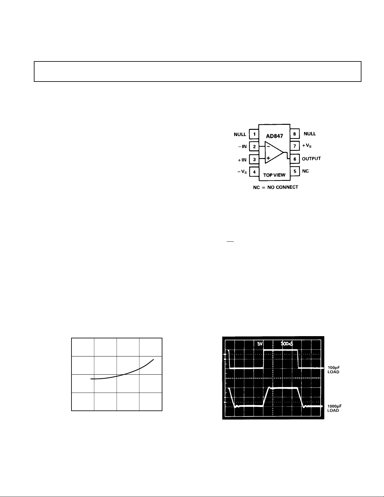
CONNECTION DIAGRAM
Plastic DIP (N),
Small Outline (R) and
Cerdip (Q) Packages
specifications which include an open-loop gain of 3500 V/V
(500 Ω load) and low input offset voltage of 0.5 mV. Commonmode rejection is a minimum of 78 dB. Output voltage swing is
±3 V into loads as low as 150 Ω. Analog Devices also offers
over 30 other high speed amplifiers from the low noise AD829
(1.7 nV/√
features 0.01% differential gain and 0.01° differential phase.
APPLICATION HIGHLIGHTS
1. As a buffer the AD847 offers a full-power bandwidth of
2. The low power and small outline package of the AD847
3. The AD847 is internally compensated for unity gain opera-
Hz) to the ultimate video amplifier, the AD811, which
12.7 MHz (5 V p-p with ±5 V supplies) making it outstanding as an input buffer for flash A/D converters.
make it very well suited for high density applications such as
multiple pole active filters.
tion and remains stable when driving any capacitive load.
6
5.5
5
4.5
QUIESCENT CURRENT – mA
4
020
Quiescent Current vs. Supply Voltage
REV. F
Information furnished by Analog Devices is believed to be accurate and
reliable. However, no responsibility is assumed by Analog Devices for its
use, nor for any infringements of patents or other rights of third parties
which may result from its use. No license is granted by implication or
otherwise under any patent or patent rights of Analog Devices.
5
SUPPLY VOLTAGE – ± Volts
10
15
AD847 Driving Capacitive Loads
One Technology Way, P.O. Box 9106, Norwood, MA 02062-9106, U.S.A.
Tel: 617/329-4700 Fax: 617/326-8703
Page 2

AD847–SPECIFICA TIONS
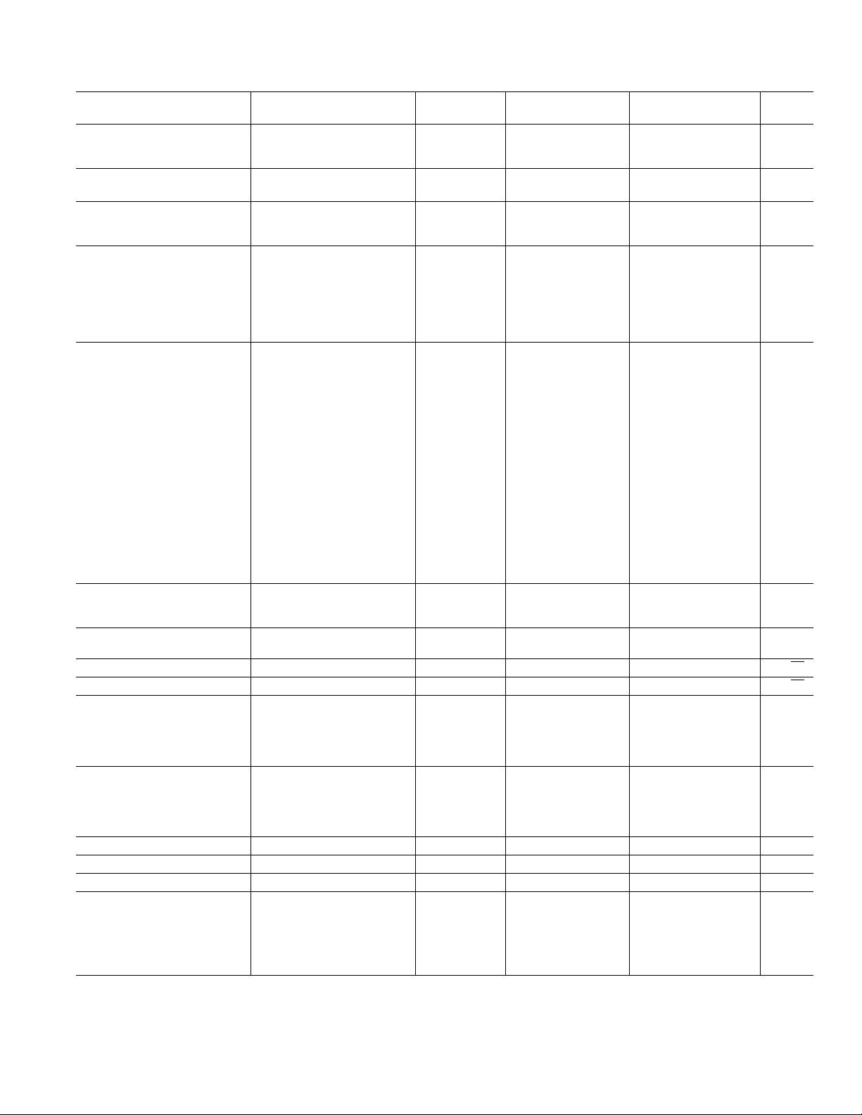
(@ TA = +258C, unless otherwise noted)
Model AD847J AD847AR
INPUT OFFSET VOLTAGE
1
Conditions V
T
to T
MIN
MAX
S
±5 V 0.5 1 0.5 1 mV
Min Typ Max Min Typ Max Units
3.5 4 mV
Offset Drift 15 15 µV/°C
INPUT BIAS CURRENT ±5 V, ± 15 V 3.3 6.6 3.3 6.6 µA
T
MIN
to T
MAX
7.2 10 µA
INPUT OFFSET CURRENT ±5 V, ± 15 V 50 300 50 300 nA
T
to T
MIN
Offset Current Drift 0.3 0.3 nA/°C
OPEN-LOOP GAIN V
V
MAX
= ±2.5 V ±5 V
OUT
R
= 500 Ω 2 3.5 2 3.5 V/mV
LOAD
T
to T
MIN
R
LOAD
= ±10 V ±15 V
OUT
R
LOAD
T
MAX
= 150 Ω 1.6 1.6 V/mV
= 1 kΩ 3 5.5 3 5.5 V/mV
to T
MIN
MAX
1 1 V/mV
1.5 1.5 V/mV
400 500 nA
DYNAMIC PERFORMANCE
Unity Gain Bandwidth ±5 V 35 35 MHz
Full Power Bandwidth
Slew Rate
3
2
V
= 5 V p-p
OUT
R
= 500 Ω, ±5 V 12.7 12.7 MHz
LOAD
V
= 20 V p-p,
OUT
R
= 1 kΩ±15 V 4.7 4.7 MHz
LOAD
R
= 1 kΩ±5 V 200 200 V/µs
LOAD
±15 V 50 50 MHz
±15 V 225 300 225 300 V/µs
Settling Time
to 0.1%, R
to 0.01%, R
Phase Margin C
Differential Gain f ≈ 4.4 MHz, R
Differential Phase f ≈ 4.4 MHz, R
= 250 Ω –2.5 V to +2.5 V ±5 V 65 65 ns
LOAD
= 250 Ω –2.5 V to +2.5 V ±5 V 140 140 ns
LOAD
10 V Step, AV = –1 ±15 V 65 65 ns
10 V Step, AV = –1 ±15 V 120 120 ns
= 10 pF ± 15 V
LOAD
R
= 1 kΩ 50 50 Degree
LOAD
= 1 kΩ±15 V 0.04 0.04 %
LOAD
= 1 kΩ±15 V 0.19 0.19 Degree
LOAD
COMMON-MODE REJECTION VCM = ±2.5 V ±5 V 78 95 78 95 dB
VCM = ±12 V ±15 V 78 95 78 95 dB
T
MIN
to T
MAX
75 75 dB
POWER SUPPLY REJECTION VS = ±5 V to ± 15 V 75 86 75 86 dB
T
MIN
to T
MAX
72 72 dB
INPUT VOLTAGE NOISE f = 10 kHz ±15 V 15 15 nV/√Hz
INPUT CURRENT NOISE f = 10 kHz ±15 V 1.5 1.5 pA/√Hz
INPUT COMMON-MODE
VOLTAGE RANGE ± 5 V +4.3 +4.3 V
–3.4 –3.4 V
±15 V +14.3 +14.3 V
–13.4 –13.4 V
OUTPUT VOLTAGE SWING R
Short-Circuit Current ± 15 V 32 32 mA
= 500 Ω±5 V 3.0 3.6 3.0 3.6 ±V
LOAD
R
= 150 Ω±5 V 2.5 3 2.5 3 ± V
LOAD
R
= 1 kΩ±15 V 12 12 ±V
LOAD
R
= 500 Ω±15 V 10 10 ±V
LOAD
INPUT RESISTANCE 300 300 kΩ
INPUT CAPACITANCE 1.5 1.5 pF
OUTPUT RESISTANCE Open Loop 15 15 Ω
POWER SUPPLY
Operating Range 64.5 618 64.5 618 V
Quiescent Current ± 5 V 4.8 6.0 4.8 6.0 mA
T
to T
MIN
MAX
T
to T
MIN
MAX
N
OTES
l
Input Offset Voltage Specifications are guaranteed after 5 minutes at TA = +25°C.
2
Full Power Bandwidth = Slew Rate/2 π V
3
Slew Rate is measured on rising edge.
All min and max specifications are guaranteed. Specifications in boldface are 100% tested at final electrical test.
Specifications subject to change without notice.
PEAK
.
±15 V 5.3 6.3 5.3 6.3 mA
7.3 7.3 mA
7.6 7.6 mA
–2–
REV. F
Page 3
AD847
Model AD847AQ AD847S
INPUT OFFSET VOLTAGE
Offset Drift 15 15 µV/°C
1
T
to T
MIN
MAX
Conditions V
S
±5 V 0.5 1 0.5 1 mV
Min Typ Max Min Typ Max Units
44mV
INPUT BIAS CURRENT ±5 V, ± 15 V 3.3 5 3.3 5 µA
T
MIN
to T
MAX
7.5 7.5 µA
INPUT OFFSET CURRENT ±5 V, ± 15 V 50 300 50 300 nA
T
MIN
to T
MAX
400 400 nA
Offset Current Drift 0.3 0.3 nA/°C
OPEN-LOOP GAIN V
= ±2.5 V ±5 V
OUT
R
= 500 Ω 2 3.5 2 3.5 V/mV
LOAD
T
to T
MIN
R
LOAD
V
= = ±10 V ±15 V
OUT
R
LOAD
T
MAX
= 150 Ω 1.6 1.6 V/mV
= 1 kΩ 3 5.5 3 5.5 V/mV
to T
MIN
MAX
11V/mV
1.5 1.5 V/mV
DYNAMIC PERFORMANCE
Unity Gain Bandwidth ±5 V 35 35 MHz
Full Power Bandwidth
Slew Rate
3
2
V
= 5 V p-p
OUT
R
= 500 Ω, ±5 V 12.7 12.7 MHz
LOAD
V
= 20 V p-p,
OUT
R
= 1 kΩ±15 V 4.7 4.7 MHz
LOAD
R
= 1 kΩ±5 V 200 200 V/µs
LOAD
±15 V 50 50 MHz
±15 V 225 300 225 300 V/µs
Settling Time
to 0.1%, R
= 250 Ω –2.5 V to +2.5 V ±5 V 65 65 ns
LOAD
10 V Step, AV = –1 ±15 V 65 65 ns
to 0.01%, R
= 250 Ω –2.5 V to +2.5 V ±5 V 140 140 ns
LOAD
10 V Step, AV = –1 ±15 V 120 120 ns
Phase Margin C
Differential Gain f ≈ 4.4 MHz, R
Differential Phase f ≈ 4.4 MHz, R
= 10 pF ± 15 V
LOAD
R
= 1 kΩ 50 50 Degree
LOAD
= 1 kΩ±15 V 0.04 0.04 %
LOAD
= 1 kΩ±15 V 0.19 0.19 Degree
LOAD
COMMON-MODE REJECTION VCM = ±2.5 V ±5 V 80 95 80 95 dB
VCM = ±12 V ±15 V 80 95 80 95 dB
T
MIN
to T
MAX
75 75 dB
POWER SUPPLY REJECTION VS = ±5 V to ±15 V 75 86 75 86 dB
T
MIN
to T
MAX
72 72 dB
INPUT VOLTAGE NOISE f = 10 kHz ±15 V 15 15 nV/√Hz
INPUT CURRENT NOISE f = 10 kHz ±15 V 1.5 1.5 pA/√Hz
INPUT COMMON-MODE
VOLTAGE RANGE ± 5 V +4.3 +4.3 V
–3.4 –3.4 V
±15 V +14.3 +14.3 V
–13.4 –13.4 V
OUTPUT VOLTAGE SWING R
Short-Circuit Current ± 15 V 32 32 mA
= 500 Ω±5 V 3.0 3.6 3.0 3.6 ±V
LOAD
R
= 150 Ω±5 V 2.5 3 2.5 3 ±V
LOAD
R
= 1 kΩ±15 V 12 12 ±V
LOAD
R
= 500 Ω±15 V 10 10 ±V
LOAD
INPUT RESISTANCE 300 300 kΩ
INPUT CAPACITANCE 1.5 1.5 pF
OUTPUT RESISTANCE Open Loop 15 15 Ω
POWER SUPPLY
Operating Range 64.5 618 64.5 618 V
Quiescent Current ± 5 V 4.8 5.7 4.8 5.7 mA
T
to T
MIN
MAX
T
to T
MIN
MAX
±15 V 5.3 6.3 5.3 6.3 mA
7.0 7.8 mA
7.6 8.4 mA
REV. F
–3–
Page 4

AD847
ABSOLUTE MAXIMUM RATINGS
Supply Voltage . . . . . . . . . . . . . . . . . . . . . . . . . . . . . . . . ±18 V
Internal Power Dissipation
2
1
Plastic (N) . . . . . . . . . . . . . . . . . . . . . . . . . . . . . . 1.2 Watts
Small Outline (R) . . . . . . . . . . . . . . . . . . . . . . . . . 0.8 Watts
Cerdip (Q) . . . . . . . . . . . . . . . . . . . . . . . . . . . . . . 1.1 Watts
Input Voltage . . . . . . . . . . . . . . . . . . . . . . . . . . . . . . . . . . .±V
S
Differential Input Voltage . . . . . . . . . . . . . . . . . . . . . . . .±6 V
Storage Temperature Range (Q) . . . . . . . . . –65°C to +150°C
(N, R) . . . . . . . . . . . . . . . . . . . . . . . . . . . –65°C to +125°C
Junction Temperature . . . . . . . . . . . . . . . . . . . . . . . . . .175°C
Lead Temperature Range (Soldering 60 sec) . . . . . . . +300°C
NOTES
1
Stresses above those listed under “Absolute Maximum Ratings” may cause
permanent damage to the device. This is a stress rating only, and functional
operation of the device at these or any other conditions above those indicated in
the operational section of this specification is not implied. Exposure to absolute
maximum rating conditions for extended periods may affect device reliability.
2
Mini-DIP Package: θJA = 100°C/Watt; θJC = 33°C/Watt
Cerdip Package: θJA = 110°C/Watt; θJC = 30°C/Watt
Small Outline Package: θJA = 155°C/Watt; θJC = 33°C/Watt
METALIZATION PHOTOGRAPH
Contact factory for latest dimensions.
Dimensions shown in inches and (mm).
ESD SUSCEPTIBILITY
ESD (electrostatic discharge) sensitive device. Electrostatic
charges as high as 4000 volts, which readily accumulate on the
human body and on test equipment, can discharge without detection. Although the AD847 features proprietary ESD protection circuitry, permanent damage may still occur on these
devices if they are subjected to high energy electrostatic discharges. Therefore, proper ESD precautions are recommended
to avoid any performance degradation or loss of functionality.
ORDERING GUIDE
Temperature Package Package
Models* Range – 8C Description Option
AD847JN 0 to +70 Plastic N-8
AD847JR 0 to +70 SOIC R-8
AD847AQ –40 to +85 Cerdip Q-8
AD847AR –40 to +85 SOIC R-8
AD847SQ –55 to +125 Cerdip Q-8
AD847SQ/883B –55 to +125 Cerdip Q-8
5962-8964701PA –55 to +125 Cerdip Q-8
*AD847 also available in J and S grade chips, and AD847JR and AD847AR are available
*in tape and reel.
–4–
REV. F
Page 5

AD847
Typical Characteristics
20
15
10
5
INPUT COMMON-MODE RANGE – ± Volts
0
020
5
SUPPLY VOLTAGE – ± Volts
(@ +258C and VS = 615 V, unless otherwise noted)
+V
IN
–V
IN
10 15
Figure 1. Input Common-Mode Range vs. Supply Voltage
30
25
20
15
±15 V SUPPLIES
20
15
+V
OUT
10
–V
OUT
5
OUTPUT VOLTAGE SWING – Volts
0
020
5
SUPPLY VOLTAGE – ± Volts
R = 500Ω
LOAD
10
15
Figure 2. Output Voltage Swing vs. Supply Voltage
6
5.5
5
10
5
OUTPUT VOLTAGE SWING – Volts p-p
0
10
100
LOAD RESISTANCE – Ω
±5V SUPPLIES
1k
10k
Figure 3. Output Voltage Swing vs. Load Resistance
5
4
V = ± 5V
S
3
INPUT BIAS CURRENT – µA
2
–60 140–40 12010080604020
–20
0
TEMPERATURE – °C
Figure 5. Input Bias Current vs. Temperature
4.5
QUIESCENT CURRENT – mA
4
020
5
SUPPLY VOLTAGE – ± Volts
10 15
Figure 4. Quiescent Current vs. Supply Voltage
100
10
1
OUTPUT IMPEDANCE – Ω
0.1
0.01
10k 100M
100k
1M 10M
FREQUENCY – Hz
Figure 6. Output Impedance vs. Frequency
REV. F
–5–
Page 6

AD847–Typical Characteristics
100
–20
100M
40
0
1k
20
100
80
60
10M1M100k10k
+100°
+80°
+60°
+40°
+20°
0
PHASE MARGIN – DEGREES
FREQUENCY – Hz
OPEN -LOOP GAIN – dB
±15V SUPPLIES
±5V SUPPLIES
1kΩ LOAD
500Ω LOAD
100
0
100M
60
20
10k
40
1k
80
10M1M100k
+SUPPLY
–SUPPLY
FREQUENCY – Hz
POWER SUPPLY REJECTION – dB
(@ +258C and VS = 615 V, unless otherwise noted)
7
6
5
4
QUIESCENT CURRENT – mA
3
–40–60
TEMPERATURE – °C
V = ± 5V
S
120100806040200–20
Figure 7. Quiescent Current vs. Temperature
52
51
50
140
35
30
25
20
SHORT CIRCUIT CURRENT LIMIT – mA
15
–40–60
AMBIENT TEMPERATURE – °C
140
120100806040200–20
Figure 8. Short-Circuit Current Limit vs. Temperature
49
UNITY – GAIN BANDWIDTH – MHz
48
–60 140
–40
Figure 9. Gain Bandwidth Product vs. Temperature
80
75
70
65
60
OPEN-LOOP GAIN – dB
55
50
10
Figure 11. Open-Loop Gain vs. Load Resistance
TEMPERATURE – °C
100
LOAD RESISTANCE – Ω
V = ±15V
S
V = ± 5V
S
100 120806040200–20
Figure 10. Open-Loop Gain and Phase Margin
vs. Frequency
1k
10k
Figure 12. Power Supply Rejection vs. Frequency
–6–
REV. F
Page 7

AD847
–70
–130
100 100k
–90
–110
1k 10k
–80
–100
–120
HARMONIC DISTORTION – dB
FREQUENCY – Hz
3V RMS
R =1kΩ
L
2ND HARMONIC
3RD HARMONIC
100
80
60
CMR – dB
40
20
0
1k
10k
V = ±1V p-p
CM
FREQUENCY – Hz
10M1M100k
100M
Figure 13. Common-Mode Rejection vs. Frequency
10
8
6
4
2
0
–2
–4
–6
OUTPUT SWING FROM 0 TO ± V
–8
–10
0
20
0.1%
1%
1% 0.1%
SETTLING TIME – ns
160
140120100806040
Figure 15. Output Swing and Error vs. Settling Time
30
25
20
R = 1kΩ
10M
L
100M
15
10
OUTPUT VOLTAGE – Volts p–p
5
0
1M
INPUT FREQUENCY – Hz
Figure 14. Large Signal Frequency Response
Figure 16. Harmonic Distortion vs. Frequency
50
40
30
20
10
INPUT VOLTAGE NOISE – nV/ Hz
0
Figure 17. Input Voltage Noise Spectral Density
REV. F
10
100
FREQUENCY – Hz
450
400
350
300
SLEW RATE – V/µs
250
200
150
–40
10M
1M100k10k1k
–60
–20
0
TEMPERATURE – °C
140
120806040 10020
Figure 18. Slew Rate vs. Temperature
–7–
Page 8

AD847
Figure 19. Inverting Amplifier Configuration
Figure 19a. Inverter Large
Signal Pulse Response
Figure 20. Noninverting Amplifier Configuration
Figure 19b. Inverter Small
Signal Pulse Response
Figure 20a. Noninverting
Large Signal Pulse Response
–8–
Figure 20b. Noninverting
Small Signal Pulse Response
REV. F
Page 9

C
F
–IN
+IN
NULL 1 NULL 8
OUTPUT
+V
S
–V
S
OFFSET NULLING
The input offset voltage of the AD847 is very low for a high
speed op amp, but if additional nulling is required, the circuit
shown in Figure 21 can be used.
Figure 21. Offset Nulling
INPUT CONSIDERATIONS
An input resistor (RIN in Figure 20) is required in circuits where
the input to the AD847 will be subjected to transient or continuous overload voltages exceeding the ±6 V maximum differential limit. This resistor provides protection for the input
transistors by limiting the maximum current that can be forced
into their bases.
For high performance circuits it is recommended that a resistor
(R
in Figures 19 and 20) be used to reduce bias current errors
B
by matching the impedance at each input. The offset voltage error will be reduced by more than an order of magnitude.
THEORY OF OPERATION
The AD847 is fabricated on Analog Devices’ proprietary
complementary bipolar (CB) process which enables the construction of pnp and npn transistors with similar f
s in the
T
600 MHz to 800 MHz region. The AD847 circuit (Figure 22)
includes an npn input stage followed by fast pnps in the folded
cascode intermediate gain stage. The CB pnps are also used in
the current amplifying output stage. The internal compensation
capacitance that makes the AD847 unity gain stable is provided
by the junction capacitances of transistors in the gain stage.
The capacitor, C
, in the output stage mitigates the effect of ca-
F
pacitive loads. At low frequencies and with low capacitive
loads, the gain from the compensation node to the output is
very close to unity. In this case C
is bootstrapped and does not
F
contribute to the compensation capacitance of the part. As the
capacitive load is increased, a pole is formed with the output
impedance of the output stage. This reduces the gain, and
therefore, C
contributes to the compensation capacitance, and the unity gain
bandwidth falls. As the load capacitance is increased, the bandwidth continues to fall, and the amplifier remains stable.
is incompletely bootstrapped. Some fraction of C
F
F
AD847
Figure 22. AD847 Simplified Schematic
GROUNDING AND BYPASSING
In designing practical circuits with the AD847, the user must
remember that whenever high frequencies are involved, some
special precautions are in order. Circuits must be built with
short interconnect leads. A large ground plane should be used
whenever possible to provide a low resistance, low inductance
circuit path, as well as minimizing the effects of high frequency
coupling. Sockets should be avoided because the increased
interlead capacitance can degrade bandwidth.
Feedback resistors should be of low enough value to assure that
the time constant formed with the capacitance at the amplifier
summing junction will not limit the amplifier performance.
Resistor values of less than 5 kΩ are recommended. If a larger
resistor must be used, a small (<10 pF) feedback capacitor in
parallel with the feedback resistor, R
sate for the input capacitances and optimize the dynamic performance of the amplifier.
Power supply leads should be bypassed to ground as close as
possible to the amplifier pins. Ceramic disc capacitors of
0.1 µF are recommended.
, may be used to compen-
F
REV. F
–9–
Page 10

AD847
VIDEO LINE DRIVER
The AD847 functions very well as a low cost, high speed line
driver for either terminated or unterminated cables. Figure 23
shows the AD847 driving a doubly terminated cable in a follower configuration.
The termination resistor, R
, (when equal to the cable’s charac-
T
teristic impedance) minimizes reflections from the far end of the
cable. While operating from ±5 V supplies, the AD847 maintains a typical slew rate of 200 V/µs, which means it can drive a
±1 V, 30 MHz signal into a terminated cable.
+V
S
75Ω
COAX
V
IN
75Ω
R
100Ω
IN
AD847
–V
S
SEE TABLE I
C
0.1 µF
0.1 µF
C
500Ω
500Ω
R
75Ω
75Ω
COAX
BT
R
75Ω
V
OUT
T
Figure 23. Video Line Driver
Table I. Video Line Driver Performance Chart
Over-
VIN*V
SUPPLYCC
–3 dB BWshoot
0 dB or ±500 mV Step ±15 20 pF 23 MHz 4%
0 dB or ±500 mV Step ±15 15 pF 21 MHz 0%
0 dB or ±500 mV Step ±15 0 pF 13 MHz 0%
0 dB or ±500 mV Step ±5 20 pF 18 MHz 2%
0 dB or ±500 mV Step ±5 15 pF 16 MHz 0%
0 dB or ±500 mV Step ±5 0 pF 11 MHz 0%
*–3 dB bandwidth numbers are for the 0 dBm signal input. Overshoot numbers
are the percent overshoot of the 1 volt step input.
A back-termination resistor (RBT, also equal to the characteristic
impedance of the cable) may be placed between the AD847 output and the cable input, in order to damp any reflected signals
caused by a mismatch between R
and the cable’s characteristic
T
impedance. This will result in a flatter frequency response, although this requires that the op amp supply ± 2 V to the output
in order to achieve a ±1 V swing at resistor R
.
T
Figure 24 shows the AD847 driving 100 pF and 1000 pF loads.
Figure 24. AD847 Driving Capacitive Loads
FLASH ADC INPUT BUFFER
The 35 MHz unity gain bandwidth of the AD847 makes it an
excellent choice for buffering the input of high speed flash A/D
converters, such as the AD9048.
Figure 25 shows the AD847 as a unity inverter for the input to
the AD9048.
0.1
–5.2V
2k
27
100
2N3906
5
0.1µF
R
R
B
AD9048
EE
+5.0V
T
D1
(MSB)
D8
(LSB)
V
CC
43Ω
V
IN
CONVERT
V
0.1µF 0.1µF
–5.2V
ANALOG
INPUT
(0V TO +2V)
TTL
CONVERT
SIGNAL
1.5kΩ
50Ω
AD589
10kΩ
0.1
AD741
1k 1k
1.5kΩ
AD847
Figure 25. Flash ADC Input Buffer
–10–
REV. F
Page 11

AD847
A High Speed, Three Op-Amp In-Amp
The circuit of Figure 26 lends itself well to CCD imaging and
other video speed applications. It uses two high speed CB process op-amps: Amplifier A3, the output amplifier, is an AD847.
+15V
10µF
COMM
10µF
–15V
1/2
AD827
–V
IN
+V
IN
3
1
A1
2
1kΩ
2kΩ
R
G
1kΩ
6
A2
5
1/2
2kΩ
5pF
7
AD827
+V
S
0.1µF
0.1µF
–V
S
2–8pF
SETTLING TIME
AC CMR ADJUST
2kΩ
2
A3
3
AD847
1.87kΩ
DC CMR
ADJUST
200Ω
The input amplifier (A1 and A2) is an AD827, which is a dual
version of the AD847. This circuit has the optional flexibility of
both dc and ac trims for common-mode rejection, plus the ability to adjust for minimum settling time.
EACH
AMPLIFIER
1µF
1µF
V
OUT
6
CIRCUIT GAIN = + 1
0.1µF
0.1µF
R
L
2kΩ
2000Ω
R
PIN 7 AD847,
PIN 8 AD827
PIN 4
AD847 & AD827
INPUT
FREQUENCY
100Hz
1kHz
10kHz
100kHz
1MHz
G
CMRR
88.3dB
87.4dB
86.2dB
67.4dB
47.1dB
BANDWIDTH, SETTLING TIME AND TOTAL HARMONIC DISTORTION VS. GAIN
THD + NOISE
GAIN R
1
2
10
100
G
OPEN
2kΩ
226Ω
20Ω
C
ADJ
(pF)
2–8
2–8
2–8
2–8
SMALL
SIGNAL
BANDWIDTH
16.1MHz
14.7MHz
4.5MHz
660kHz
SETTLING
TIME
TO 0.1%
200ns
200ns
370ns
2.5µs
BELOW INPUT
LEVEL
@ 10kHz
82dB
82dB
81dB
71dB
Figure 26. A High Speed In-Amp Circuit for Data Acquisition
REV. F
–11–
Page 12

AD847
HIGH SPEED DAC BUFFER
The wide bandwidth and fast settling time of the AD847 makes
it a very good output buffer for high speed current-output D/A
converters like the AD668. As shown in Figure 27, the op amp
establishes a summing node at ground for the DAC output. The
output voltage is determined by the amplifier’s feedback resistor
+15V
10µF
0.1µF
DIGITAL
INPUTS
10
11
12
1
2
3
4
5
6
7
8
9
MSB
REFCOM
AD668
LSB
V
REFIN1
REFIN2
I
OUT
R
LOAD
ACOM
LCOM
IBPO
V
THCOM
VTH
24
CC
23
22
21
20
19
18
17
16
15
EE
14
100pF
13
(10.24 V for a 1 kΩ resistor). Note that since the DAC generates a positive current to ground, the voltage at the amplifier
output will be negative. A 100 Ω series resistor between the
noninverting amplifier input and ground minimizes the offset
effects of op amp input bias currents.
TO ANALOG
GROUND PLANE
–
1V NOMINAL
REFERENCE INPUT
+
10k
100Ω
ANALOG GROUND PLANE
0.1µF
1kΩ
10µF
1k
AD847
–15V
+5V
ANALOG
OUTPUT
ANALOG
SUPPLY
GROUND
C1191f–10–9/92
Mini-DIP (N-8) Package
8
PIN 1
1
0.39 (9.91) MAX
0.165±0.01
(4.19±0.25)
0.125
(3.18)
MIN
0.018±0.003
(0.46±0.08)
0.10
(2.54)
BSC
0.30 (7.62)
REF
0.011±0.003
(0.28±0.08)
15
°
0
°
4
0.033
(0.84)
NOM
5
0.25
(6.35)
0.035±0.01
(0.89±0.25)
0.18±0.03
(4.57±0.76)
SEATING
PLANE
0.31
(7.87)
Figure 27. High Speed DAC Buffer
OUTLINE DIMENSIONS
Dimensions shown in inches and (mm).
Cerdip (Q-8) Package
0.005 (0.13) MIN
PIN 1
0.200
(5.08)
MAX
0.200 (5.08)
0.125 (3.18)
0.023 (0.58)
0.014 (0.36)
0.055 (1.40) MAX
8
1
0.405 (10.29) MAX
0.100
(2.54)
BSC
0.320 (8.13)
0.290 (7.37)
0.015 (0.38)
0.008 (0.20)
15°
0°
5
4
0.070 (1.78)
0.030 (0.76)
0.310 (7.87)
0.220 (5.59)
0.060 (1.52)
0.015 (0.38)
0.150
(3.81)
MIN
SEATING
PLANE
Small Outline (R-8) Package
0.150 (3.81)
0.244 (6.20)
0.228 (5.79)
0.010 (0.25)
0.004 (0.10)
0.020 (0.051) x 45
CHAMF
0.098 (0.2482)
0.075 (0.1905)
PIN 1
8
°
0
°
8
1
0.197 (5.01)
0.189 (4.80)
0.050
(1.27)
BSC
10
0
0.019 (0.48)
0.014 (0.36)
°
0.190 (4.82)
0.170 (4.32)
°
°
5
0.157 (3.99)
0.150 (3.81)
4
0.102 (2.59)
0.094 (2.39)
0.030 (0.76)
0.018 (0.46)
0.090
(2.29)
PRINTED IN U.S.A.
All brand or product names mentioned are trademarks or registered trademarks of their respective holders.
–12–
REV. F
 Loading...