

Datasheet AD843JR-16, AD843JN, AD843JCHIPS, AD843BQ, AD843BH Datasheet (Analog Devices)
...Page 1
34 MHz, CBFET
a
FEATURES
AC PERFORMANCE
Unity Gain Bandwidth: 34 MHz
Fast Settling: 135 ns to 0.01%
Slew Rate: 250 V/ms
Stable at Gains of 1 or Greater
Full Power Bandwidth: 3.9 MHz
DC PERFORMANCE
Input Offset Voltage: 1 mV max (AD843K/B}
Input Bias Current: 0.6 nA typ
Input Voltage Noise: 19 nV/√
Open Loop Gain: 30 V/mV into a 500 V Load
Output Current: 50 mA min
Supply Current: 13 mA max
Available in 8-Pin Plastic Mini-DIP & Cerdip, 16-Pin SOIC,
20-Pin LCC and 12-Pin Hermetic Metal Can Packages
Available in Tape and Reel in Accordance with
EIA-481A Standard
Chips and MIL-STD-883B Parts Also Available
APPLICATIONS
High Speed Sample-and-Hold Amplifiers
High Bandwidth Active Filters
High Speed Integrators
High Frequency Signal Conditioning
Hz
Fast Settling Op Amp
AD843
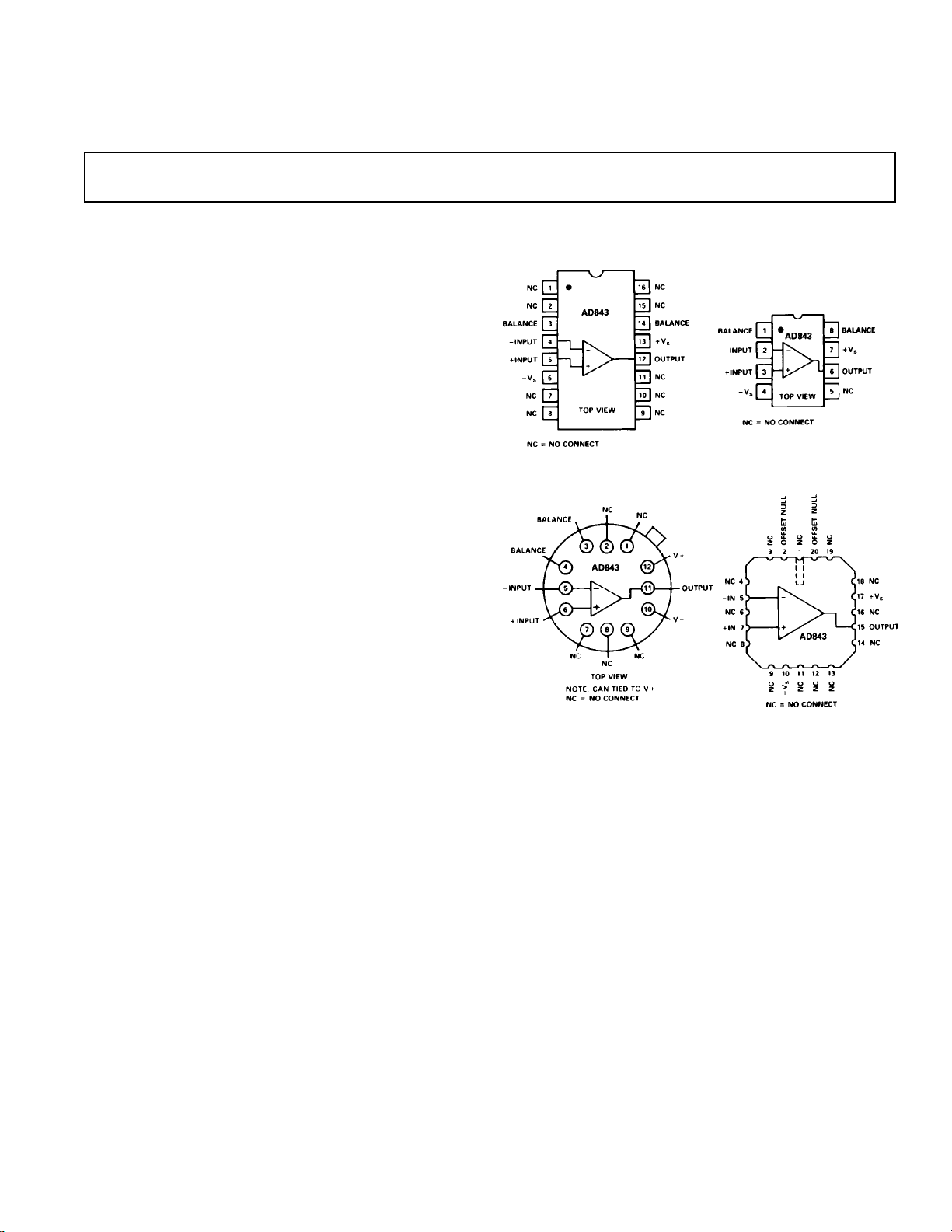
CONNECTION DIAGRAMS
16-Pin SOIC (R-16) Package Plastic (N-8) and
Cerdip (Q-8) Package
TO-8 (H-12A) Package LCC (E-20A) Package
PRODUCT DESCRIPTION
The AD843 is a fast settling, 34 MHz, CBFET input op amp.
The AD843 combines the low (0.6 nA) input bias currents
characteristic of a FET input amplifier while still providing a
34 MHz bandwidth and a 135 ns settling time (to within 0.01%
of final value for a 10 volt step). The AD843 is a member of the
Analog Devices’ family of wide bandwidth operational amplifiers. These devices are fabricated using Analog Devices’ junction
isolated complementary bipolar (CB) process. This process permits a combination of dc precision and wideband ac performance previously unobtainable in a monolithic op amp.
The 250 V/µs slew rate and 0.6 nA input bias current of the
AD843 ensure excellent performance in high speed sample-andhold applications and in high speed integrators. This amplifier is
also ideally suited for high bandwidth active filters and high frequency signal conditioning circuits.
Unlike many high frequency amplifiers, the AD843 requires no
external compensation and it remains stable over its full operating temperature range. It is available in five performance grades:
the AD843J and AD843K are rated over the commercial
temperature range of 0°C to +70°C. The AD843A and AD843B
are rated over the industrial temperature range of –40°C to +85°C.
The AD843S is rated over the military temperature range of –55°C
to +125°C and is available processed to MIL-STD-883B, Rev. C.
REV. D
Information furnished by Analog Devices is believed to be accurate and
reliable. However, no responsibility is assumed by Analog Devices for its
use, nor for any infringements of patents or other rights of third parties
which may result from its use. No license is granted by implication or
otherwise under any patent or patent rights of Analog Devices.
The AD843 is offered in either 8-pin plastic DIP or hermetic
cerdip packages, in 16-pin SOIC, 20-Pin LCC, or in a 12-pin
metal can. Chips are also available.
PRODUCT HIGHLIGHTS
1. The high slew rate, fast settling time and low input bias current of the AD843 make it the ideal amplifier for 12-bit D/A
and A/D buffers, for high speed sample-and-hold amplifiers
and for high speed integrator circuits. The AD843 can replace many FET input hybrid amplifiers such as the
LH0032, LH4104 and OPA600.
2. Fully differential inputs provide outstanding performance in
all standard high frequency op amp applications such as signal conditioning and active filters.
3. Laser wafer trimming reduces the input offset voltage to
1 mV max (AD843K and AD843B).
4. Although external offset nulling is unnecessary in many applications, offset null pins are provided.
5. The AD843 does not require external compensation at
closed loop gains of 1 or greater.
© Analog Devices, Inc., 1995
One Technology Way, P.O. Box 9106, Norwood. MA 02062-9106, U.S.A.
Tel: 617/329-4700 Fax: 617/326-8703
Page 2

AD843–SPECIFICATIONS
(@ TA = +25°C and ±15 V dc, unless otherwise noted)
AD843J/A AD843K/B AD843S
1
Model Conditions Min Typ Max Min Typ Max Min Typ Max Units
INPUT OFFSET VOLTAGE
Offset Drift 12 12 35 12 µV/°C
INPUT BIAS CURRENT Initial (TJ = +25°C) 50 40 50 pA
INPUT OFFSET CURRENT Initial (TJ = +25°C) 30 20 30 pA
INPUT CHARACTERISTICS
Input Resistance 10
1
T
MIN-TMAX
Warmed-Up
T
MIN-TMAX
Warmed-Up
T
MIN-TMAX
2
2
1.0 2.0 0.5 1.0 1.0 2.0 mV
1.7 4.0 1.2 2.0 3.0 4.5 mV
0.8 2.5 0.6 1.0 0.8 2.5 nA
60/160 23/65 2600 nA
0.25 1.0 0.2 0.4 0.25 1.0 nA
23/64 9/26 1025 nA
10
10
10
10
10
Ω
Input Capacitance 6 6 6 pF
INPUT VOLTAGE RANGE
Common Mode 610 +12, 610 +12, 610 +12, V
–13 –13 –13
COMMON-MODE REJECTION VCM = ±10 V 60 72 70 76 60 72 dB
T
MIN-TMAX
60 72 68 76 60 72 dB
INPUT VOLTAGE NOISE f = 10 kHz 19 19 19 nV/√Hz
Wideband Noise 10 Hz to 10 MHz 60 60 60 µV rms
OPEN LOOP GAIN VO = ±10 V
R
≥ 500 Ω 15 25 20 30 15 30 V/mV
LOAD
T
MIN-TMAX
10 20 10 25 10 25 V/mV
OUTPUT CHARACTERISTICS
Voltage R
Current V
Output Resistance Open Loop 12 12 12 Ω
≥ 500 Ω 610 +11.5, 610 +11.5, 610 +11.5, V
LOAD
= ±10 V 50 50 50 mA
OUT
–12.6 –12.6 –12.6
FREQUENCY RESPONSE
Unity Gain Bandwidth V
Full Power Bandwidth
3
= 90 mV p-p 34 34 34 MHz
OUT
VO = 20 V p-p
R1 ≥ 500 Ω 2.5 3.9 2.5 3.9 2.5 3.9 MHz
Rise Time A
Overshoot A
Slew Rate A
Settling Time 10 V Step
= –1 10 10 10 ns
VCL
= –1 15 15 15 %
VCL
= –1 160 250 160 250 160 250 V/µs
VCL
A
= –1
VCL
to 0.1% 95 95 95 ns
to 0.01% 135 135 135 ns
Overdrive Recovery –Overdrive 200 200 200 ns
+Overdrive 700 700 700 ns
Differential Gain f = 4.4 MHz 0.025 0.025 0.025 %
Differential Phase f = 4.4 MHz 0.025 0.025 0.025 Degree
POWER SUPPLY
Rated Performance ± 15 ±15 ±15 V
Operating Range 64.5 618 64.5 618 64.5 618 V
Quiescent Current 12 13 12 13 12 13 mA
T
Rejection Ratio ±5 V to ±18 V 65 76 70 80 65 76 dB
Rejection Ratio T
MIN-TMAX
MIN-TMAX
12.3 14 12.3 14 12.5 16 mA
62 76 68 80 62 76 dB
TEMPERATURE RANGE
Operating, Rated Performance
Commercial (0°C to +70°C) AD843J AD843K
Industrial (–40°C to +85°C) AD843A AD843B
Military (–55°C to +125°C)
4
AD843S
PACKAGE OPTIONS
Plastic (N-8) AD843JN AD843KN
Cerdip (Q-8) AD843AQ AD843BQ AD843SQ, AD843SQ/883B
Metal Can (H-12A) AD843BH AD843SH, AD843SH/883B
LCC (E-20A) AD843SE/883B
SOIC (R-16) AD843JR–16
Tape & Reel AD843JR-16–REEL
AD843JR-16–REEL7
Chips AD843JCHIPS AD843SCHIPS
–2–
REV. D
Page 3
AD843
NOTES
1
Standard Military Drawings Available: 5962-9098001M2A (SE/883B), 5962-9098001MXA (SH/883B), 5962-9098001MPA (SQ/883B).
2
Specifications are guaranteed after 5 minutes at TA = +25°C.
3
Full power bandwidth = Slew Rate/2 πV peak.
4
All “S” grade T
Specifications subject to change without notice.
Specifications in boldface are tested on all production units at final electrical test. Results from those tests are used to calculate outgoing quality levels. All min and
max specifications are guaranteed although only those shown in boldface are tested on all production units.
MIN-TMAX
specifications are tested with automatic test equipment at TA = –55°C and TA = +125°C.
ABSOLUTE MAXIMUM RATINGS
Supply Voltage . . . . . . . . . . . . . . . . . . . . . . . . . . . . . . . . .±18 V
Internal Power Dissipation
2
1
Plastic Package . . . . . . . . . . . . . . . . . . . . . . . . . . 1.50 Watts
Cerdip Package . . . . . . . . . . . . . . . . . . . . . . . . . 1.35 Watts
12-Pin Header Package . . . . . . . . . . . . . . . . . . . 1.80 Watts
16-Pin SOIC Package . . . . . . . . . . . . . . . . . . . . 1.50 Watts
20-Pin LCC Package . . . . . . . . . . . . . . . . . . . . . . 1.00 Watt
Input Voltage . . . . . . . . . . . . . . . . . . . . . . . . . . . . . . . . . . ±V
S
Output Short Circuit Duration . . . . . . . . . . . . . . . . Indefinite
Differential Input Voltage . . . . . . . . . . . . . . . . . . +V
and –V
S
S
Storage Temperature Range (N, R) . . . . . . . –65°C to +125°C
Storage Temperature Range (Q, H, E) . . . . –65°C to +150°C
Operating Temperature Range
AD843J/R . . . . . . . . . . . . . . . . . . . . . . . . . . . 0°C to +70°C
AD843A/B . . . . . . . . . . . . . . . . . . . . . . . . . –40°C to +85°C
AD843S . . . . . . . . . . . . . . . . . . . . . . . . . . –55°C to +125°C
Lead Temperature Range (Soldering 60 sec) . . . . . . . . +300°C
ESD Rating . . . . . . . . . . . . . . . . . . . . . . . . . . . . . . . . . . 500 V
NOTES
1
Stresses above those listed under “Absolute Maximum Ratings” may cause
permanent damage to the device at these or any other conditions above those
indicated in the operational sections of this specification is not implied. Exposure
to absolute maximum rating conditions for extended periods may affect device
reliability.
2
8-Pin Plastic Package: θJA = 100°C/Watt
8-Pin Cerdip Package: θJA = 110°C/Watt
12-Pin Header Package: θJA = 80°C/Watt
16-Pin SOIC Package: θJA = 100°C/Watt
20-Pin LCC Package: θJA = 150°C/Watt
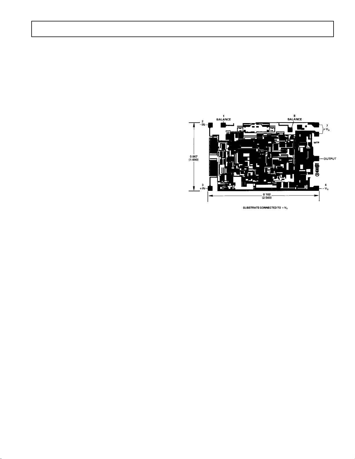
METALIZATION PHOTOGRAPH
Contact factory for latest dimensions.
Dimensions shown in inches and (mm).
REV. D
–3–
Page 4
AD843–Typical Characteristics
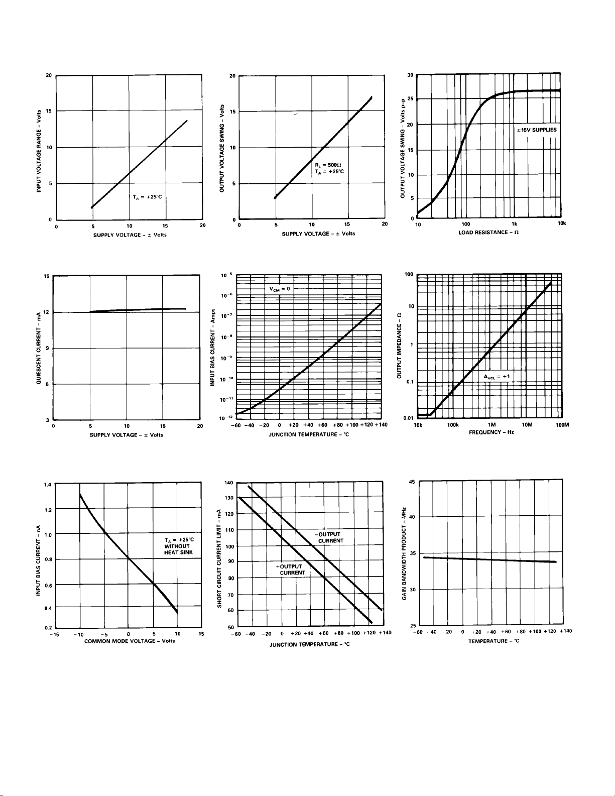
Figure 1. Input Voltage Range vs.
Supply Voltage
Figure 4. Quiescent Current vs.
Supply Voltage
Figure 2. Output Voltage Swing vs.
Supply Voltage
Figure 5. Input Bias Current vs.
Junction Temperature
Figure 3. Output Voltage Swing vs.
Load Resistance
Figure 6. Output Impedance vs.
Frequency
Figure 7. Input Bias Current vs.
Common Mode Voltage
Figure 8. Short Circuit Current
Limit vs. Junction Temperature (T
–4–
Figure 9. Gain Bandwidth Product
)
J
vs. Temperature
REV. D
Page 5

AD843
Figure 10. Open Loop Gain and Phase
Margin vs. Frequency
Figure 13. Common Mode
Rejection vs. Frequency
Figure 11. Open Loop Gain vs.
Supply Voltage
Figure 14. Large Signal Frequency
Response
Figure 12. Power Supply Rejection vs.
Frequency
Figure 15. Output Swing and Error
vs. Settling Time
Figure 16. Harmonic Distortion
vs. Frequency
REV. D
Figure 17. Input Noise Voltage
Spectral Density
–5–
Figure 18. Slew Rate vs.
Temperature
Page 6

AD843–Typical Characteristics
Figure 19. Open Loop Gain vs.
Resistive Load
Figure 20c. Inverter Small Signal
Pulse Response. C
= 0, CL = 10 pF
F
Figure 20a. Inverting Amplifier
Connection
Figure 20d. Inverter Large Signal
Pulse Response. C
= 5 pF, CL = 110 pF
F
Figure 20b. Inverter Large Signal
Pulse Response. C
= 0, CL = 10 pF
F
Figure 20e. Inverter Small Signal
Pulse Response. C
= 5 pF, CL = 110 pF
F
Figure 21a. Unity Gain Inverter
Circuit for Driving Capacitive
Loads
Figure 21b. Inserter Cap Load
Large Signal Pulse Response.
= 15 pF, CL = 410 pF
C
F
–6–
Figure 21c. Inverter Cap Load
Small Signal Pulse Response.
= 15 pF, CL = 410 pF
C
F
REV. D
Page 7

AD843
Figure 22a. Unity Gain Buffer
Amplifier
Figure 23a. Unity Gain Buffer Circuit
for Driving Capacitive Loads
Figure 22b. Buffer Large
Signal Pulse Response.
CL = 10 pF
Figure 23b. Buffer Cap Load
Large Signal Pulse Response.
= 33 pF, CL = 10 pF
C
F
Figure 22c. Buffer Small
Signal Pulse Response.
CL = 10 pF
Figure 23c. Buffer Cap Load Small
Signal Pulse Response. C
C
= 10 pF
L
= 33 pF,
F
REV. D
Figure 23d. Buffer Cap Load
Large Signal Pulse Response.
= 33 pF, CL = 110 pF
C
F
Figure 23e. Buffer Cap Load
Small Signal Pulse Response.
CF = 33 pF, CL = 110 pF
–7–
Page 8

AD843
GROUNDING AND BYPASSING
Like most high bandwidth amplifiers, the AD843 is sensitive to
capacitive loading. Although it will drive capacitive loads up to
20 pF without degradation of its rated performance, both an
increased capacitive load drive capability and a “cleaner”
(nonringing) pulse response can be obtained from the AD843
by using the circuits illustrated in Figures 20 to 23. The addition of a 5 pF feedback capacitor to the unity gain inverter connection (Figure 20a) substantially reduces the circuit’s
overshoot, even when it is driving a 110 pF load. This can be
seen by comparing the waveforms of Figures 20b through 20e.
To drive capacitive loads greater than 100 pF, the load should
be decoupled from the amplifier’s output by a 10 Ω resistor and
the feedback capacitor, C
, should be connected directly be-
F
tween the amplifier’s output and its inverting input (Figure
21a). When using a 15 pF feedback capacitor, this circuit can
drive 400 pF with less than 20% overshoot, as illustrated in Figures 21b and 21c. Increasing capacitor C
to 47 pF also in-
F
creases the capacitance drive capability to 1000 pF, at the
expense of a 10:1 reduction in bandwidth compared with the
simple unity gain inverter circuit of Figure 20a.
Unity gain voltage followers (buffers) are more sensitive to
capacitive loads than are inverting amplifiers because there is no
attenuation of the feedback signal. The AD843 can drive 10 pF
to 20 pF when connected in the basic unity gain buffer circuit
of Figure 22a.
The 1 kΩ resistor in series with the AD843’s noninverting input
serves two functions: first, together with the amplifier’s input
capacitance, it forms a low-pass filter which slows down the
actual signal seen by the AD843. This helps reduce ringing on
the amplifier’s output voltage. The resistor’s second function is
to limit the current into the amplifier when the differential input
voltage exceeds the total supply voltage.
The AD843 will deliver a much “cleaner” pulse response when
connected in the somewhat more elaborate follower circuit of
Figure 23a. Note the reduced overshoot in Figure 23b and 23c
as compared to Figures 22b and 22c.
For maximum bandwidth, in most applications, input and feedback resistors used with the AD843 should have resistance values equal to or less than 1.5 kΩ. Even with these low resistance
values, the resultant RC time constant formed between them
and stray circuit capacitances is large enough to cause peaking
in the amplifier’s response. Adding a small capacitor, C
F
, as
shown in Figures 20a to 23a will reduce this peaking and flatten
the overall frequency response. C
will normally be less than
F
10 pF in value.
The AD843 can drive resistive loads over the range of 500 Ω to
∞ with no change in dynamic response. While a 499 Ω load was
used in the circuits of Figures 20-23, the performance of these
circuits will be essentially the same even if this load is removed
or changed to some other value, such as 2 kΩ.
To obtain the “cleanest” possible transient response when driving heavy capacitive loads, be sure to connect bypass capacitors
directly between the power supply pins of the AD843 and
ground as outlined in “grounding and bypassing.”
GROUNDING AND BYPASSING
In designing practical circuits using the AD843, the user must
keep in mind that some special precautions are needed when
dealing with high frequency signals. Circuits must be wired using short interconnect leads. Ground planes should be used
whenever possible to provide both a low resistance, low inductance circuit path and to minimize the effects of high frequency
coupling. IC sockets should be avoided, since their increased
interlead capacitance can degrade the bandwidth of the device.
Power supply leads should be bypassed to ground as close as
possible to the pins of the amplifier. Again, the component leads
should be kept very short. As shown in Figure 24, a parallel
combination of a 2.2 µF tantalum and a 0.1 µF ceramic disc ca-
pacitor is recommended.
Figure 24. Recommended Power Supply Bypassing for
the AD843 (DIP Pinout)
USING A HEAT SINK
The AD843 consumes less quiescent power than most precision
high speed amplifiers and is specified to operate without using a
heat sink. However, when driving low impedance loads, the current applied to the load can be 4 to 5 times greater than the quiescent current. This will produce a noticeable temperature rise,
which will increase input bias currents. The use of a small heat
sink, such as the Mouser Electronics #33HS008 is recommended.
Offset Null Configuration (DIP Pinout)
–8–
REV. D
Page 9

AD843
SAMPLE-AND-HOLD AMPLIFIER CIRCUITS
A Fast Switching Sample & Hold Circuit
A sample-and-hold circuit possessing short acquisition time and
low aperture delay can be built using an AD843 and discrete
JFET switches. The circuit of Figure 25 employs five n-channel
JFETs (with turn-on times of 35 ns) and an AD843 op amp
(which can settle to 0.01% in 135 ns). The circuit has an aperture delay time of 50 ns and an acquisition time of 1 µs or less.
This circuit is based on a noninverting open loop architecture,
using a differential hold capacitor to reduce the effects of pedestal error. The charge that is removed from CH1 by Q2 and Q3
is offset by the charge removed from CH2 by Q4 and Q5. This
circuit can tolerate low hold capacitor values (approximately
100 pF), which improve acquisition time, due to the small gateto-drain capacitance of the discrete JFETs. Although pedestal
error will vary with input signal level, making trimming more
difficult, the circuit has the advantages of high bandwidth and
short acquisition times. In addition, it will exhibit some
nonlinearity because both amplifiers are operating with a common-mode input. Amplifier A2, however, contributes less than
0.025% linearity error, due to its 72 dB common-mode rejection ratio.
To make sure the circuit accommodates a wide ± 10 V input
range, the gates of the JFETs must be connected to a potential
near the –15 V supply. The level-shift circuitry (diode D3, PNP
transistor Q7, and NPN transistor Q6) shifts the TTL level S/H
command to provide for an adequate pinch-off voltage for the
JFET switches over the full input voltage range.
The JFETs Q2, Q3, Q4 and Q5 across the two hold capacitors
ensure signal acquisition for all conditions of V
when the circuit switches from the sample to the hold mode.
Transistor Q1 provides an extra stage of isolation between the
output of amplifier A1 and the hold capacitor CH1.
When selecting capacitors for use in a sample-and-hold circuit,
the designer should choose those types with low dielectric
absorption and low temperature coefficients. Silvered-mica
capacitors exhibit low (0 to 100 ppm/°C) temperature coefficients and will still work in temperatures exceeding 200°C. It is
also recommend that the user test the chosen capacitor to insure
that its value closely matches that printed on it since not all
capacitors are fully tested by their manufacturers for absolute
tolerance.
and V
IN
OUT
Figure 25. A Fast Switching Sample-and-Hold Amplifier
A PING-PONG S/H AMPLIFIER
For improved throughput over the circuit of Figure 25, a “pingpong” architecture may be used. A ping-pong circuit overcomes
some of the problems associated with high speed S/H amplifiers
by allowing the use of a larger hold capacitor for a given sample
rate: this will reduce the associated feedthrough, droop and pedestal errors.
Figure 26 illustrates a simple, four-chip ping-pong sample-andhold amplifier circuit. This design increases throughput by using
one channel to acquire a new sample while another channel
holds the previous sample. Instead of having to reacquire the
signal when switching from hold to sample mode, it alternately
connects the outputs from Channel 1 or from Channel 2 to the
A/D converter. In this case, the throughput is the slew rate and
settling time of the output amplifiers, A2 and A3.
REV. D
–9–
A high speed CB amplifier, A1, follows the input signal. U1, a
dual wideband “T” switch, connects the input buffer amp to
one of the two output amplifiers while selecting the complementary amplifier to drive the A/D input. For example, when
“select” is at logic high, A1 drives CH1, A2 tracks the input signal and the output of A3 is connected to the input of the A/D
converter. At the same time, A3 holds an analog value and its
output is connected to the input of the A/D converter. When the
select command goes to logic LOW, the two output amplifiers
alternate functions.
Since the input to the A/D converter is the alternated “held”
outputs from A1 and A2, the offset voltage mismatch of the two
amplifiers will show up as nonlinearity and, therefore, distortion
in the output signal. To minimize this, potentiometers can be
used to adjust the offsets of the output amplifiers until they are
Page 10

AD843
equal. Alternatively, an autocalibration circuit using two D/A
converters can be employed. This can also be used to calibrate
out the effects of offset voltage drift over temperature.
The switch choice, for U1s, is critical in this type of design. The
DG542 utilizes “T” switching techniques on each channel for
exceptionally low crosstalk and for high isolation. The part fur-
ther improves these specifications by using ground pins between
the signal pins. With an input frequency of 5 MHz, crosstalk
and isolation are –85 dB and –75 dB, respectively. A limitation
of this switch is that it operates from a maximum –5 V negative
supply, making bipolar operation more difficult. It is recommended that amplifiers A1, A2 and A3 operate from the same
–5 V supply to minimize any potential latch-up problems.
Figure 26. A Ping-Pong Sample-and-Hold Amplifier
Figure 27. Settling Time Test Circuit
–10–
REV. D
Page 11

AD843
MEASURING AD843 SETTLING TIME
Figure 28 shows the dynamic response of the AD843 while operating in the settling time test circuit of Figure 27. The input of
the settling time fixture is driven by a flat-top pulse generator.
The error signal output from A1, the AD843 under test, is amplified by op amp A2 and then clamped by two high speed
Schottky diodes.
Figure 28. Settling Characteristics: +10 V to 0 V Step.
Upper Trace: Amplified Error Voltage (0.01%/Div)
Lower Trace: Output of AD843 Under Test (5 V/Div)
The error signal is clamped to prevent it from greatly overloading the oscilloscope preamp. A Tektronix oscilloscope preamp
type 7A26 was chosen because it will recover from the approximately 0.4 volt overload, quickly enough to allow accurate measurement of the AD843’s 135 ns settling time. Amplifier A2 is a
very high speed op amp; it provides a voltage gain of 10, providing a total gain of 5 from the error signal to the oscilloscope input.
detector’s output (top trace) loses slightly over a volt of the
8 volt peak input value (bottom trace) in 75 ms, or a rate of
approximately 16 µV/µs.
Figure 30. Peak Detector Response to 125 Hz Pulse Train
A FAST PEAK DETECTOR CIRCUIT
The peak detector circuit of Figure 29, can accurately capture
the amplitude of input pulses as narrow as 200 ns and can hold
their value with a droop rate of less than 20 µV/µs. This circuit
will capture the peak value of positive polarity waveforms; to
detect negative peaks, simply reverse the polarity of the two
diodes.
The high bandwidth and 200 V/µs slew rate of amplifier A2, an
AD843, allows the detector’s output to “keep up” with its input
thus minimizing overshoot. The low (<1 nA) input current of
the AD843 ensures that the droop rate is limited only by the
reverse leakage of diode D2, which is typically <10 nA for the
type shown. The low droop rate is apparent in Figure 30. The
Figure 31. Peak Capture Time
Amplifier A1, an AD847, can drive 680 pF hold capacitor, CP,
fast enough to “catch-up” with the next peak in 100 ns and still
settle to the new value in 250 ns, as illustrated in Figure 31.
Reducing the value of capacitor C
to 100 pF will maximize the
P
speed of this circuit at the expense of increased overshoot and
droop. Since the AD847 can drive an arbitrarily large value of
capacitance, C
can be increased to reduce droop, at the expense
P
of response time.
REV. D
Figure 29. A Fast Peak Detector Circuit
–11–
Page 12

AD843
16 9
81
0.4133 (10.50)
0.3977 (10.00)
0.4193 (10.65)
0.3937 (10.00)
0.2992 (7.60)
0.2914 (7.40)
PIN 1
SEATING
PLANE
0.0118 (0.30)
0.0040 (0.10)
0.0192 (0.49)
0.0138 (0.35)
0.1043 (2.65)
0.0926 (2.35)
0.0500
(1.27)
BSC
0.0125 (0.32)
0.0091 (0.23)
0.0500 (1.27)
0.0157 (0.40)
8°
0°
0.0291 (0.74)
0.0098 (0.25)
x 45°
OUTLINE DIMENSIONS
Dimensions shown in inches and (mm).
Mini-DIP Package
(N-8)
TO-8 Package
(H-12A)
Cerdip Package
(Q-8)
C1314b–2–6/95
16-Pin SOIC Package
(R-16)
0.082 ± 0.018
(2.085 ± 0.455)
LCC Package
(E-20A)
0.350 ± 0.008 SQ
0.050
(1.27)
–12–
(8.89 ± 0.20) SQ
NO. 1 PIN
INDEX
0.040 x 45°
(1.02 x 45°)
REF 3 PLCS
0.025 ± 0.003
(0.635 ± 0.075)
0.020 x 45°
(0.51 x 45°)
REF
PRINTED IN U.S.A.
REV. D
 Loading...