

Page 1
1 nV/√Hz Low Noise
FEATURES
Low noise
1 nV/√Hz input noise
45 nV/√Hz output noise
High accuracy dc performance (AD8429BRZ)
90 dB CMRR minimum (G = 1)
50 μV maximum input offset voltage
0.02% maximum gain accuracy (G = 1)
Excellent ac specifications
80 dB CMRR to 5 kHz (G = 1)
15 MHz bandwidth (G = 1)
1.2 MHz bandwidth (G = 100)
22 V/μs slew rate
THD: −130 dBc (1 kHz, G = 1)
Versa tile
±4 V to ±18 V dual supply
Gain set with a single resistor (G = 1 to 10,000)
Temperature range for specified performance
−40°C to +125°C
Instrumentation Amplifier
AD8429
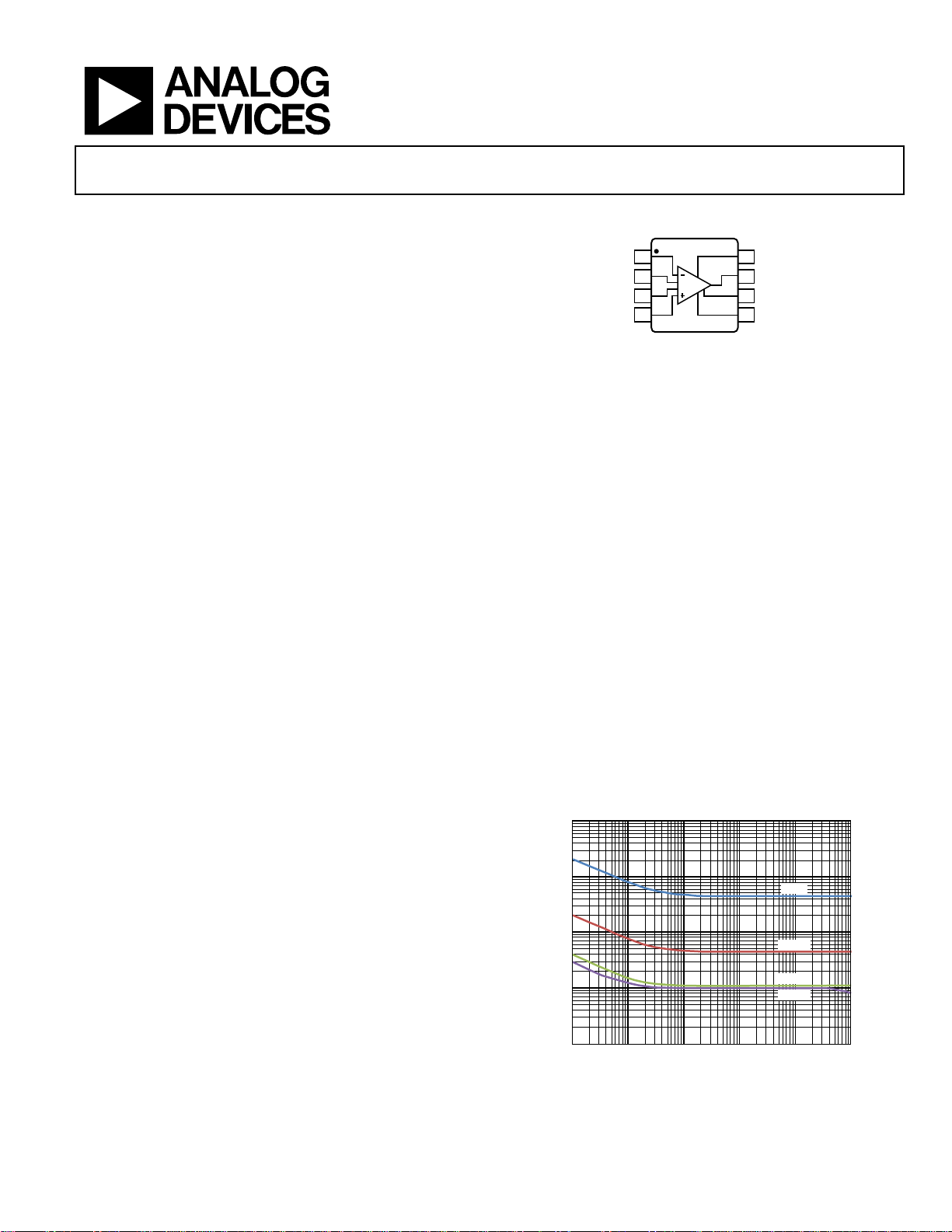
PIN CONNECTION DIAGRAM
AD8429
–IN
R
R
+IN
G
G
1
2
3
4
(Not to Scale)
TOP VIEW
Figure 1.
8
+V
S
7
V
OUT
6
REF
5
–V
S
09730-001
APPLICATIONS
Medical instrumentation
Precision data acquisition
Microphone preamplification
Vibration analysis
GENERAL DESCRIPTION
The AD8429 is an ultralow noise, instrumentation amplifier
designed for measuring extremely small signals over a wide
temperature range (−40°C to +125°C).
The AD8429 excels at measuring tiny signals. It delivers ultralow
input noise performance of 1 nV/√Hz. The high CMRR of the
AD8429 prevents unwanted signals from corrupting the acquisition. The CMRR increases as the gain increases, offering high
rejection when it is most needed. The high performance pin
configuration of the AD8429 allows it to reliably maintain high
CMRR at frequencies well beyond those of typical instrumentation
amplifiers.
The AD8429 reliably amplifies fast changing signals. Its current
feedback architecture provides high bandwidth at high gain, for
example, 1.2 MHz at G = 100. The design includes circuitry to improve settling time after large input voltage transients. The AD8429
was designed for excellent distortion performance, allowing use in
demanding applications such as vibration analysis.
Gain is set from 1 to 10,000 with a single resistor. A reference
pin allows the user to offset the output voltage. This feature can
Rev. 0
Information furnished by Analog Devices is believed to be accurate and reliable. However, no
responsibility is assumed by Anal og Devices for its use, nor for any infringements of patents or ot her
rights of third parties that may result from its use. Specifications subject to change without notice. No
license is granted by implication or otherwise under any patent or patent rights of Analog Devices.
Trademarks and registered trademarks are the property of their respective owners.
be useful to shift the output level when interfacing to a single
supply signal chain.
The AD8429 performance is specified over the extended industrial
temperature range of −40°C to +125°C. It is available in an 8-lead
plastic SOIC package.
1000
100
Hz)
10
NOISE (nV/
1
0.1
1 10 100 1k 10k 100k
Figure 2. RTI Voltage Noise Spectral Density vs. Frequency
One Technology Way, P.O. Box 9106, Norwood, MA 02062-9106, U.S.A.
Tel: 781.329.4700 www.analog.com
Fax: 781.461.3113 ©2011 Analog Devices, Inc. All rights reserved.
FREQUENCY (Hz)
G = 1
G = 10
G = 100
G = 1k
09730-002
Page 2

AD8429
TABLE OF CONTENTS
Features.............................................................................................. 1
Applications....................................................................................... 1
Pin Connection Diagram ................................................................ 1
General Description......................................................................... 1
Revision History ...............................................................................2
Specifications..................................................................................... 3
Absolute Maximum Ratings............................................................ 6
Thermal Resistance...................................................................... 6
ESD Caution.................................................................................. 6
Pin Configuration and Function Descriptions............................. 7
Typical Performance Characteristics............................................. 8
Theory of Operation ......................................................................15
REVISION HISTORY
4/11—Revision 0: Initial Version
Architecture ................................................................................ 15
Gain Selection............................................................................. 15
Reference Terminal.................................................................... 15
Input Voltage Range................................................................... 16
Layout .......................................................................................... 16
Input Bias Current Return Path ............................................... 17
Input Protection ......................................................................... 17
Radio Frequency Interference (RFI)........................................ 17
Calculating the Noise of the Input Stage................................. 18
Outline Dimensions....................................................................... 19
Ordering Guide .......................................................................... 19
Rev. 0 | Page 2 of 20
Page 3

AD8429
SPECIFICATIONS
VS = ±15 V, V
Table 1.
A Grade B Grade
Parameter Test Conditions/Comments Min Typ Max Min Typ Max Unit
COMMON-MODE REJECTION
RATIO (CMRR)
CMRR DC to 60 Hz with 1 kΩ
Source Imbalance
G = 1 80 90 dB
G = 10 100 110 dB
G = 100 120 130 dB
G = 1000 134 140 dB
CMRR at 5 kHz VCM = ±10 V
G = 1 76 80 dB
G = 10 90 90 dB
G = 100 90 90 dB
G = 1000 90 90 dB
VOLTAGE NOISE, RTI VIN+, VIN− = 0 V
Spectral Density1: 1 kHz
Input Voltage Noise, eni 1.0 1.0 nV/√Hz
Output Voltage Noise, eno 45 45 nV/√Hz
Peak to Peak: 0.1 Hz to 10 Hz
G = 1 2 2 μV p-p
G = 1000 100 100 nV p-p
CURRENT NOISE
Spectral Density: 1 kHz 1.5 1.5 pA/√Hz
Peak to Peak: 0.1 Hz to 10 Hz 100 100 pA p-p
VOLTAGE OFFSET2
Input Offset, V
Average TC 0.1 1 0.1 0.3 μV/°C
Output Offset, V
Average TC 3 10 3 10 μV/°C
Offset RTI vs. Supply (PSR) VS = ±5 V to ±15 V
G = 1 90 100 dB
G = 10 110 120 dB
G = 100 130 130 dB
G = 1000 130 130 dB
INPUT CURRENT
Input Bias Current 300 150 nA
Average TC 250 250 pA/°C
Input Offset Current 100 30 nA
Average TC 15 15 pA/°C
DYNAMIC RESPONSE
Small Signal Bandwidth: –3 dB
G = 1 15 15 MHz
G = 10 4 4 MHz
G = 100 1.2 1.2 MHz
G = 1000 0.15 0.15 MHz
= 0 V, TA = 25°C, G = 1, RL = 10 k, unless otherwise noted.
REF
VCM = ±10 V
150 50 μV
OSI
1000 500 μV
OSO
Rev. 0 | Page 3 of 20
Page 4

AD8429
A Grade B Grade
Parameter Test Conditions/Comments Min Typ Max Min Typ Max Unit
Settling Time 0.01% 10 V step
G = 1 0.75 0.75 μs
G = 10 0.65 0.65 μs
G = 100 0.85 0.85 μs
G = 1000 5 5 μs
Settling Time 0.001% 10 V step
G = 1 0.9 0.9 μs
G = 10 0.9 0.9 μs
G = 100 1.2 1.2 μs
G = 1000 7 7 μs
Slew Rate
G = 1 to 100 22 22 V/μs
THD First five harmonics, f = 1 kHz,
= 2 kΩ, V
R
L
= 10 V p-p
OUT
G = 1 −130 −130 dBc
G = 10 −116 −116 dBc
G = 100 −113 −113 dBc
G = 1000 −111 −111 dBc
THD + N f = 1 kHz, RL = 2 kΩ, V
OUT
=
10 V p-p
G = 100 0.0005 0.0005 %
GAIN3 G = 1 + (6 kΩ/RG)
Gain Range 1 10000 1 10000 V/V
Gain Error V
= ±10 V
OUT
G = 1 0.05 0.02 %
G > 1 0.3 0.15 %
Gain Nonlinearity V
= −10 V to +10 V
OUT
G = 1 to 1000 RL = 10 kΩ 2 2 ppm
Gain vs. Temperature
G = 1 2 5 2 5 ppm/°C
G > 1 −100 −100 ppm/°C
INPUT
Impedance (Pin to Ground)4 1.5||3 1.5||3 GΩ||pF
Input Operating Voltage
Range
5
V
= ±4 V to ±18 V −VS + 2.8 +VS − 2.5 −VS + 2.8 +VS − 2.5 V
S
OUTPUT
Output Swing RL = 2 kΩ −VS + 1.8 +Vs − 1.2 −VS + 1.8 +Vs − 1.2 V
Over Temperature −VS + 1.9 +Vs − 1.3 −VS + 1.9 +Vs − 1.3 V
Output Swing RL = 10 kΩ −VS + 1.7 +Vs − 1.1 −VS + 1.7 +Vs − 1.1 V
Over Temperature −VS + 1.8 +Vs − 1.2 −VS + 1.8 +Vs − 1.2 V
Short-Circuit Current 35 35 mA
REFERENCE INPUT
RIN 10 10 kΩ
IIN V
+, VIN− = 0 V 70 70 μA
IN
Voltage Range −VS +VS V
Reference Gain to Output 1 1 V/V
Reference Gain Error 0.01 0.05 0.01 0.05 %
Rev. 0 | Page 4 of 20
Page 5

AD8429
A Grade B Grade
Parameter Test Conditions/Comments Min Typ Max Min Typ Max Unit
POWER SUPPLY
Operating Range ±4 ±18 ±4 ±18 V
Quiescent Current 6.7 7 6.7 7 mA
T = 125°C 9 9 mA
TEMPERATURE RANGE
For Specified Performance −40 +125 −40 +125 °C
1
Total voltage noise = √(e
2
Total RTI VOS = (V
3
These specifications do not include the tolerance of the external gain setting resistor, RG. For G > 1, add RG errors to the specifications given in this table.
4
Differential and common-mode input impedance can be calculated from the pin impedance: Z
5
Input voltage range of the AD8429 input stage only. The input range can depend on the common-mode voltage, differential voltage, gain, and reference voltage.
See the section for more details. Input Voltage Range
OSI
) + (V
2
+ (eno/G)2 + e
ni
/G).
OSO
2
). See the Theory of Operation section for more information.
RG
DIFF
= 2(Z
); ZCM = Z
PIN
/2.
PIN
Rev. 0 | Page 5 of 20
Page 6
AD8429
ABSOLUTE MAXIMUM RATINGS
Table 2.
Parameter Rating
Supply Voltage ±18 V
Output Short-Circuit Current Duration Indefinite
Maximum Voltage at –IN, +IN1 ±VS
Differential Input Voltage
Gain ≤ 4 ±VS
4 > Gain > 50 ±50 V/gain
Gain ≥ 50 ±1 V
Maximum Voltage at REF ±VS
Storage Temperature Range −65°C to +150°C
Specified Temperature Range −40°C to +125°C
Maximum Junction Temperature 140°C
ESD
Human Body Model 3.0 kV
Charge Device Model 1.5 kV
Machine Model 0.2 kV
1
For voltages beyond these limits, use input protection resistors. See the
Theory of Operation section for more information.
1
Stresses above those listed under Absolute Maximum Ratings
may cause permanent damage to the device. This is a stress
rating only; functional operation of the device at these or any
other conditions above those indicated in the operational
section of this specification is not implied. Exposure to absolute
maximum rating conditions for extended periods may affect
device reliability.
THERMAL RESISTANCE
θJA is specified for a device in free air using a 4-layer JEDEC
printed circuit board (PCB).
Table 3.
Package θJA Unit
8-Lead SOIC 121 °C/W
ESD CAUTION
Rev. 0 | Page 6 of 20
Page 7

AD8429
PIN CONFIGURATION AND FUNCTION DESCRIPTIONS
AD8429
1
–IN
2
R
G
3
R
G
4
+IN
TOP VIEW
(Not to Scale)
Figure 3. Pin Configuration
Table 4. Pin Function Descriptions
Pin No. Mnemonic Description
1 −IN Negative Input Terminal.
2, 3 RG Gain Setting Terminals. Place resistor across the RG pins to set the gain. G = 1 + (6 kΩ/RG).
4 +IN Positive Input Terminal.
5 −VS Negative Power Supply Terminal.
6 REF Reference Voltage Terminal. Drive this terminal with a low impedance voltage source to level shift the output.
7 V
Output Terminal.
OUT
8 +VS Positive Power Supply Terminal.
8
+V
S
7
V
OUT
6
REF
5
–V
S
09730-003
Rev. 0 | Page 7 of 20
Page 8

AD8429
TYPICAL PERFORMANCE CHARACTERISTICS
T = 25°C, VS = ±15, V
15
G = 1
10
5
0
= 0, RL = 10 kΩ, unless otherwise noted.
REF
VS = ±15V
V
= ±12V
S
V
= ±5V
S
160
140
120
100
GAIN = 1000
GAIN = 100
GAIN = 10
GAIN = 1
80
–5
COMMON-MODE VOLTAGE (V)
–10
–15
–15 –10 –5 0 5 10 15
OUTPUT VOLTAGE (V)
Figure 4. Input Common-Mode Voltage vs. Output Voltage,
Dual Supply, V
15
G = 100
10
5
0
–5
COMMON-MODE VOLTAGE (V)
–10
–15
–15 –10 –5 0 5 10 15
= ±5 V, ±12 V, ±15 V (G = 1)
S
VS = ±15V
V
= ±12V
S
V
= ±5V
S
OUTPUT VOLTAGE (V)
Figure 5. Input Common-Mode Voltage vs. Output Voltage,
Dual Supply, V
0
–5
–10
–15
–20
–25
–30
–35
INPUT BIAS CURRENT (nA)
–40
–45
–50
–12.28V
–14 –12 –10 –8 –6 –4 –2 0 2 4 6 8 10 12 14
= ±5 V, ±12 V, ±15 V (G = 100)
S
COMMON-MODE VOLTAGE (V)
Figure 6. Input Bias Current vs. Common-Mode Voltage
+12.60V
60
POSITIVE PSRR (dB)
40
20
0
1 10 100 1k 10k 100k 1M
09730-010
FREQUENCY (Hz)
09730-069
Figure 7. Positive PSRR vs. Frequency
160
140
120
100
80
60
NEGATIVE PSRR (dB)
40
20
0
1 10 100 1k 10k 100k 1M
09730-011
FREQUENCY (Hz)
GAIN = 1000
GAIN = 100
GAIN = 10
GAIN = 1
09730-070
Figure 8. Negative PSRR vs. Frequency
70
GAIN = 1000
60
50
GAIN = 100
40
30
GAIN = 10
20
GAIN (dB)
10
GAIN = 1
0
–10
–20
–30
100 1k 10k 100k 1M 10M 100M
09730-068
FREQUENCY (Hz)
VS = ±15V
09730-017
Figure 9. Gain vs. Frequency
Rev. 0 | Page 8 of 20
Page 9

AD8429
160
G = 1k
140
G = 100
G = 10
120
G = 1
100
80
CMRR (dB)
60
40
20
BANDWIDTH
LIMITED
40
30
20
10
0
INPUT BIAS CURRENT (nA)
–10
IB+
IB–
I
3.0
OS
2.5
2.0
1.5
1.0
INPUT OFFSET CURRENT ( nA)
0.5
0
10 100 1k 10k 100k 1M
1
FREQUENCY (Hz)
Figure 10. CMRR vs. Frequency
140
G = 1k
120
G = 10
100
G = 1
80
60
CMRR (dB)
40
20
0
1 10 100 1k 10k 1M100k
G = 100
BANDWIDTH
FREQUENCY (Hz)
Figure 11. CMRR vs. Frequency, 1 kΩ Source Imbalance
12
10
8
6
4
2
CHANGE IN INPUT OFFSET VOLTAGE (µV)
0
0 100 200 300 400 500 600 700
WARM-UP TIME (s)
Figure 12. Change in Input Offset Voltage (V
) vs. Warm-Up Time
OSI
LIMITED
–20
–45 –15 15 45 75 105 13 5–30 0 30 60 90 120
09730-110
TEMPERATURE ( °C)
0
09730-019
Figure 13. Input Bias Current and Input Offset Current vs. Temperature
40
30
20
10
0
–10
–20
CMRR (µV/V)
–30
–40
–50
NORMALIZED AT 25°C
–60
–40 –25 –10 5 20 35
09730-111
TEMPERATURE (°C)
50 65 80 95 110 125
GAIN = 1
09730-114
Figure 14. CMRR vs. Temperature (G = 1), Normalized at 25°C
10.0
9.5
9.0
8.5
8.0
7.5
7.0
6.5
SUPPLY CURRENT (mA)
6.0
5.5
5.0
–50 –10 1301109070503010–30
09730-112
TEMPERATURE (° C)
09730-022
Figure 15. Supply Current vs. Temperature (G = 1)
Rev. 0 | Page 9 of 20
Page 10

AD8429
V
V
V
50
40
30
20
10
0
–10
–20
–30
SHORT-CIRCUIT CURRENT (mA)
–40
–50
–40 –25 –10 5 20 35 50 65 80 95 110 125
Figure 16. Short-Circuit Current vs. Temperature (G = 1)
30
25
20
15
10
SLEW RATE (V/µs)
5
0
–40 –25 –10 5 20 35 50 65 80 95 110 125
Figure 17. Slew Rate vs. Temperature, V
25
20
15
10
SLEW RATE (V/µs)
5
0
–40 –25 –10 5 20 35 50 65 80 95 110 125
Figure 18. Slew Rate vs. Temperature, V
–SR
+SR
–SR
+SR
I
SHORT+
I
SHORT–
TEMPERATURE ( °C)
TEMPERATURE ( °C)
TEMPERATURE ( °C)
= ±15 V (G = 1)
S
= ±5 V (G = 1)
S
+
S
–0.5
–1.0
–1.5
–2.0
–2.5
+2.5
+2.0
INPUT VOLTAGE (V)
+1.5
+1.0
REFERRED TO SUPPLY VOLTAGES
+0.5
–V
S
411614121086
09730-023
SUPPLY VOLTAGE (±VS)
+125°C
+85°C
+25°C
–40°C
8
09730-026
Figure 19. Input Voltage Limit vs. Supply Voltage
+
S
–0.4
–0.8
–1.2
+2.0
+1.6
INPUT VOLTAGE (V)
+1.2
+0.8
REFERRED TO SUPPLY VOLTAGES
+0.4
–V
S
411614121086
09730-024
SUPPLY VOLTAGE (±VS)
Figure 20. Output Voltage Swing vs. Supply Voltage, R
+
S
–0.4
–0.8
–1.2
+2.0
+1.6
INPUT VOLTAGE (V)
+1.2
+0.8
REFERRED TO SUPPLY VOLTAGES
+0.4
–V
S
411614121086
09730-025
SUPPLY VOLTAGE (±VS)
Figure 21. Output Voltage Swing vs. Supply Voltage, R
+125°C
+85°C
+25°C
–40°C
8
09730-027
= 10 kΩ
L
+125°C
+85°C
+25°C
–40°C
= 2 kΩ
L
8
09730-028
Rev. 0 | Page 10 of 20
Page 11

AD8429
V
15
VS = ±15V
10
5
0
–5
OUTPUT VOLTAGE SWING (V)
–10
–15
100 100k10k1k
LOAD ()
Figure 22. Output Voltage Swing vs. Load Resistance
+
S
VS = ±15V
–0.4
–0.8
–1.2
–1.6
+125°C
+85°C
+25°C
–40°C
09730-029
10
8
6
4
2
0
–2
–4
NONLINEARITY (ppm/DIV)
–6
–8
–10
–10–8–6–4–20246810
OUTPUT VO LTAGE (V )
Figure 25. Gain Nonlinearity (G = 1000), R
1000
100
GAIN = 1000
= 10 kΩ
L
G = 1
9730-084
+2.0
+1.6
+1.2
OUTPUT VOLTAGE SWING (V)
+0.8
REFERRED TO SUPPLY VOLTAGES
+0.4
–V
S
10µ 10m1m100µ
OUTPUT CURRENT (A)
Figure 23. Output Voltage Swing vs. Output Current
10
8
6
4
2
0
–2
–4
NONLINEARITY (ppm/DIV)
–6
–8
–10
–10–8–6–4–20246810
OUTPUT VOLTAGE (V)
Figure 24. Gain Nonlinearity (G = 1), R
= 10 kΩ
L
+125°C
+85°C
+25°C
–40°C
GAIN = 1
10
NOISE (nV/Hz)
1
0.1
1 10 100 1k 10k 100k
09730-030
FREQUENCY (Hz)
G = 10
G = 100
G = 1k
09730-126
Figure 26. RTI Voltage Noise Spectral Density vs. Frequency
GAIN = 1000, 100nV/DIV
GAIN = 1, 2V/DIV
1s/DIV
09730-083
09730-086
Figure 27. 0.1 Hz to 10 Hz RTI Voltage Noise (G = 1, G = 1000)
Rev. 0 | Page 11 of 20
Page 12

AD8429
16
15
14
13
12
11
10
9
8
7
NOISE (pA/ Hz)
6
5
4
3
2
1
1 10 100 1k 10k 100k
Figure 28. Current Noise Spectral Density vs. Frequency
FREQUENCY (Hz)
5V/DIV
750ns TO 0. 01%
872ns TO 0. 001%
0.002%/DIV
2µs/DIV
TIME (µs)
09730-087
09730-090
Figure 31. Large Signal Pulse Response and Settling Time (G = 1), 10 V Step,
= ±15 V
V
S
5V/DIV
50pA/DIV
1s/DIV
Figure 29. 0.1 Hz to 10 Hz Current Noise
30
= ±15V
V
S
25
20
15
10
OUTPUT VOLTAGE (V p-p)
VS = ±5V
5
0
100 1k 10k 100k 1M 10M
FREQUENCY (Hz)
Figure 30. Large Signal Frequency Response
G = 1
640ns TO 0.01%
896ns TO 0. 001%
0.002%/DIV
09730-088
TIME (µs)
2µs/DIV
09730-091
Figure 32. Large Signal Pulse Response and Settling Time (G = 10), 10 V Step,
= ±15 V
V
S
5V/DIV
840ns TO 0.01%
1152ns TO 0. 001%
0.002%/DIV
2µs/DIV
TIME (µs)
09730-089
09730-040
Figure 33. Large Signal Pulse Response and Settling Time (G = 100),
10 V Step, V
= ±15 V
S
Rev. 0 | Page 12 of 20
Page 13

AD8429
G = 100
5V/DIV
5.04µs TO 0.01%
6.96µs TO 0.001%
0.002%/DIV
10µs/DIV
TIME (µs)
09730-041
Figure 34. Large Signal Pulse Response and Settling Time (G = 1000),
10 V Step, V
G = 1
50mV/DIV
Figure 35. Small Signal Response (G = 1), R
= ±15 V
S
1µs/DIV
= 10 kΩ, CL = 100 pF
L
09730-042
G = 10
20mV/DIV
Figure 37. Small Signal Response (G = 100), R
G = 1000
20mV/DIV
Figure 38. Small Signal Response (G = 1000), R
1µs/DIV
= 10 kΩ, CL = 100 pF
L
10µs/DIV
= 10 kΩ, CL = 100 pF
L
G = 1
09730-044
09730-045
20mV/DIV
Figure 36. Small Signal Response (G = 10), R
1µs/DIV
= 10 kΩ, CL = 100 pF
L
09730-043
Rev. 0 | Page 13 of 20
NO LOAD
C
= 100pF
L
C
= 147pF
L
1µs/DIV50mV/DIV
9730-093
Figure 39. Small Signal Response with Various Capacitive Loads (G = 1),
R
= Infinity
L
Page 14

AD8429
1400
1200
1000
800
600
SETTLING TIME (ns)
400
200
0
2 4 6 8 10 12 14 16 18 20
1
0.1
0.01
0.001
SETTL ED TO 0.001%
SETTLED TO 0.01%
STEP SIZE (V)
Figure 40. Settling Time vs. Step Size (G = 1)
NO LOAD
2k LOAD
600 LOAD
G = 1, SECOND HARMONIC
V
OUT
= 10V p-p
1
NO LOA D
2k LOAD
600 LOAD
0.1
0.01
0.001
AMPLITUDE (Percentag e of Fu ndamental)
0.0001
10 100 1k 10k 100k
09730-092
G = 1000, SECO ND HARMONIC
FREQUENCY (Hz)
V
OUT
= 10V p-p
09730-098
Figure 43. Second Harmonic Distortion vs. Frequency (G = 1000)
1
0.1
0.01
NO LOAD
2k LOAD
600 LOAD
G = 1000, THIRD HARMONIC
V
OUT
= 10V p-p
0.0001
AMPLITUDE (Percentag e of Fu ndamenta l)
0.00001
10 100 1k 10k 100k
FREQUENCY (Hz)
Figure 41. Second Harmonic Distortion vs. Frequency (G = 1)
1
NO LOAD
2k LOAD
600 LOAD
0.1
0.01
0.001
0.0001
AMPLITUDE (Percentag e of Fu ndamental )
0.00001
10 100 1k 10k 100k
FREQUENCY (Hz)
G = 1, THIRD HARMONIC
Figure 42. Third Harmonic Distortion vs. Frequency (G = 1)
V
OUT
= 10V p-p
0.001
AMPLIT UDE (Percent age of Fundamen tal)
0.0001
10 100 1k 10k 100k
09730-096
FREQUENCY (Hz)
09730-099
Figure 44. Third Harmonic Distortion vs. Frequency (G = 1000)
1
V
= 10V p-p
OUT
R
2k
L
0.1
0.01
THD (%)
0.001
GAIN = 1000
GAIN = 10
0.0001
GAIN = 1
0.00001
10 100 1k 10k 100k
09730-097
FREQUENCY (Hz)
GAIN = 100
09730-100
Figure 45. THD vs. Frequency
Rev. 0 | Page 14 of 20
Page 15

AD8429
THEORY OF OPERATION
V
B
S
S
+V
R
G
–V
COMPENSATION
+V
S
–IN
–V
S
II
I
B
A1 A2
C1 C2
NODE 1
R1
3k
+V
RG–
–V
Figure 46. Simplified Schematic
ARCHITECTURE
The AD8429 is based on the classic 3-op-amp topology. This
topology has two stages: a preamplifier to provide differential
amplification followed by a difference amplifier that removes
the common-mode voltage and provides additional amplification. Figure 46 shows a simplified schematic of the AD8429.
The first stage works as follows. To keep its two inputs matched,
Amplifier A1 must keep the collector of Q1 at a constant voltage.
It does this by forcing RG− to be a precise diode drop from –IN.
Similarly, A2 forces RG+ to be a constant diode drop from +IN.
Therefore, a replica of the differential input voltage is placed
across the gain setting resistor, R
. The current that flows through
G
this resistance must also flow through the R1 and R2 resistors,
creating a gained differential signal between the A2 and A1
outputs.
The second stage is a G = 1 difference amplifier, composed of
Amplifier A3 and the R3 through R6 resistors. This stage removes
the common-mode signal from the amplified differential signal.
The transfer function of the AD8429 is
V
= G × (V
OUT
IN+
− V
IN−
) + V
REF
where:
G
k6
1+=
R
G
GAIN SELECTION
Placing a resistor across the R
AD8429, which can be calculated by referring to Table 5 or by
using the following gain equation:
k6
R
G
1
−=G
terminals sets the gain of the
G
I
B
COMPENSATION
R4
5k
NODE 2
R5
+V
R2
3k
S
S
Q2Q1
RG+
S
5k
+IN
–V
S
R6
5k
R3
5k
A3
+V
S
V
OUT
+V
S
–V
S
REF
–V
S
09730-058
Table 5. Gains Achieved Using 1% Resistors
1% Standard Table Value of RG Calculated Gain
6.04 kΩ 1.993
1.5 kΩ 5.000
665 Ω 10.02
316 Ω 19.99
121 Ω 50.59
60.4 Ω 100.3
30.1 Ω 200.3
12.1 Ω 496.9
6.04 Ω 994.4
3.01 Ω 1994
The AD8429 defaults to G = 1 when no gain resistor is used.
Add the tolerance and gain drift of the R
resistor to the
G
specifications of the AD8429 to determine the total gain accuracy of the system. When the gain resistor is not used, gain
error and gain drift are minimal.
RG Power Dissipation
The AD8429 duplicates the differential voltage across its inputs
onto the R
resistor. Choose an RG resistor size sufficient to
G
handle the expected power dissipation.
REFERENCE TERMINAL
The output voltage of the AD8429 is developed with respect to
the potential on the reference terminal. This is useful when the
output signal must be offset to a precise midsupply level. For
example, a voltage source can be tied to the REF pin to level
shift the output, allowing the AD8429 to drive a single-supply
ADC. The REF pin is protected with ESD diodes and should
not exceed either +V
or −VS by more than 0.3 V.
S
Rev. 0 | Page 15 of 20
Page 16

AD8429
For best performance, maintain a source impedance to the REF
terminal that is well below 1 Ω. As shown in Figure 46, the
reference terminal, REF, is at one end of a 5 k resistor.
Additional impedance at the REF terminal adds to this 5 k
resistor and results in amplification of the signal connected to
the positive input. The amplification from the additional R
can be calculated as follows:
2(5 k + R
)/(10 k + R
REF
REF
)
Only the positive signal path is amplified; the negative path
is unaffected. This uneven amplification degrades CMRR.
INCORRECT
AD8429
REF
V
Figure 47. Driving the Reference Pin
V
CORRECT
AD8429
REF
+
OP1177
–
INPUT VOLTAGE RANGE
Figure 4 and Figure 5 show the allowable common-mode input
voltage ranges for various output voltages and supply voltages.
The 3-op-amp architecture of the AD8429 applies gain in the
first stage before removing common-mode voltage with the
difference amplifier stage. Internal nodes between the first and
second stages (Node 1 and Node 2 in Figure 46) experience a
combination of a gained signal, a common-mode signal, and a
diode drop. This combined signal can be limited by the voltage
supplies even when the individual input and output signals are
not limited.
LAYOUT
To ensure optimum performance of the AD8429 at the PCB
level, care must be taken in the design of the board layout. The
pins of the AD8429 are arranged in a logical manner to aid in
this task.
1
–IN
2
R
G
3
R
G
4
+IN
AD8429
TOP VIEW
(Not to Scale)
Figure 48. Pinout Diagram
Common-Mode Rejection Ratio over Frequency
Poor layout can cause some of the common-mode signals to be
converted to differential signals before reaching the in-amp.
Such conversions occur when one input path has a frequency
response that is different from the other. To maintain high
CMRR over frequency, closely match the input source
impedance and capacitance of each path. Place additional
8
+V
S
7
V
OUT
6
REF
5
–V
S
09730-060
REF
09730-059
Rev. 0 | Page 16 of 20
source resistance in the input path (for example, for input
protection) close to the in-amp inputs, which minimizes their
interaction with parasitic capacitance from the PCB traces.
Parasitic capacitance at the gain setting pins can also affect CMRR
over frequency. If the board design has a component at the gain
setting pins (for example, a switch or jumper), choose a component
such that the parasitic capacitance is as small as possible.
Power Supplies and Grounding
Use a stable dc voltage to power the instrumentation amplifier.
Noise on the supply pins can adversely affect performance. See
the PSRR performance curves in Figure 9 and Figure 10 for more
information.
Place a 0.1 µF capacitor as close as possible to each supply pin.
Because the length of the bypass capacitor leads is critical at
high frequency, surface-mount capacitors are recommended. A
parasitic inductance in the bypass ground trace works against
the low impedance created by the bypass capacitor. As shown in
Figure 49, a 10 µF capacitor can be used farther away from the
device. For larger value capacitors, intended to be effective at
lower frequencies, the current return path distance is less critical.
In most cases, this capacitor can be shared by other precision
integrated circuits.
+V
S
REF
10µF
LOAD
V
OUT
09730-061
0.1µF
+IN
R
G
AD8429
–IN
0.1µF 10µF
–V
S
Figure 49. Supply Decoupling, REF, and Output Referred to Local Ground
A ground plane layer is helpful to reduce parasitic inductances.
This minimizes voltage drops with changes in current. The area
of the current path is directly proportional to the magnitude of
parasitic inductances and, therefore, the impedance of the path
at high frequency. Large changes in currents in an inductive
decoupling path or ground return create unwanted effects, due
to the coupling of such changes into the amplifier inputs.
Because load currents flow from the supplies, the load should
be connected at the same physical location as the bypass capacitor grounds.
Reference Pin
The output voltage of the AD8429 is developed with respect to
the potential on the reference terminal. Ensure that REF is tied
to the appropriate local ground.
Page 17

AD8429
V
V
INPUT BIAS CURRENT RETURN PATH
The input bias current of the AD8429 must have a return path to
ground. When using a floating source without a current return
path, such as a thermocouple, create a current return path, as
shown in Figure 50.
INCORRECT
+V
S
AD8429
REF
–V
S
TRANSFORMER
+V
S
AD8429
REF
–V
S
THERMOCOUPL E
+V
S
C
AD8429
C
CAPACITIVEL Y COUPLED
REF
–V
S
f
=
HIGH- PASS
2RC
CAPACITIVEL Y COUPLED
Figure 50. Creating an Input Bias Current Return Path
10M
1
CORRECT
TRANSFORMER
THERMOCOUPL E
C
R
C
R
+V
S
AD8429
–V
S
+V
S
AD8429
–V
S
+V
S
AD8429
–V
S
REF
REF
REF
INPUT PROTECTION
Do not allow the inputs of the AD8429 to exceed the ratings
stated in the Absolute Maximum Ratings section of this data
sheet. If this cannot be done, protection circuitry can be added
in front of the AD8429 to limit the current into the inputs to a
maximum current, I
Input Voltages Beyond the Rails
If voltages beyond the rails are expected, use an external resistor
in series with each input to limit current during overload conditions. The limiting resistor at the input can be computed from
R
PROTECT
≥
.
MAX
VV
MAX
SUPPLY
|| −
IN
I
Noise sensitive applications may require a lower protection resistance. Low leakage diode clamps, such as the BAV199, can be used
at the inputs to shunt current away from the AD8429 inputs,
thereby allowing smaller protection resistor values. To ensure
current flows primarily through the external protection diodes,
place a small value resistor, such as a 33 , between the diodes and
the AD8429.
+
+V
R
PROTECT
+
V
V
I
IN+
–
R
PROTECT
+
IN–
–
SIMPLE METHOD LOW NOISE METHOD
S
AD8429
–V
S
+
V
IN+
–
+
V
IN–
–
R
PROTECT
R
PROTECT
S
33
I
–V
S
+V
S
33
–V
S
Figure 51. Protection for Voltages Beyond the Rails
Large Differential Input Voltage at High Gain
If large differential voltages at high gain are expected, use an
external resistor in series with each input to limit current during
overload conditions. The limiting resistor at each input can be
computed by using the following equation:
MAX
−≥V1
⎞
⎟
R
G
⎟
⎠
⎛
V
1
DIFF
R −
PROTECT
⎜
⎜
I
2
⎝
Noise sensitive applications may require a lower protection resistance. Low leakage diode clamps, such as the BAV199, can be used
across the inputs to shunt current away from the AD8429 inputs
and, therefore, allow smaller protection resistor values.
V
+
DIFF
–
R
PROTECT
I
R
PROTECT
R
PROTECT
I
+
DIFF
–
R
PROTECT
09730-062
SIMPLE METHOD L OW NOISE METHOD
AD8429
Figure 52. Protection for Large Differential Voltages
I
MAX
The maximum current into the AD8429 inputs, I
on time and temperature. At room temperature, the device can
withstand a current of 10 mA for at least one day. This time is
cumulative over the life of the device.
RADIO FREQUENCY INTERFERENCE (RFI)
RF rectification is often a problem when amplifiers are used in
applications that have strong RF signals. The disturbance can
appear as a small dc offset voltage. High frequency signals can
be filtered with a low-pass RC network placed at the input of
the instrumentation amplifier, as shown in Figure 53.
+V
S
AD8429
–V
S
AD8429
, depends
MAX
09730-066
09730-067
Rev. 0 | Page 17 of 20
Page 18

AD8429
V
R
()(
()(
(
(
C
C
1nF
R
4.02k
4.02k
C
D
R
10nF
R
C
C
1nF
Figure 53. RFI Suppression
0.1µF
+IN
G
–IN
0.1µF
+
S
AD8429
–V
S
REF
10µF
10µF
V
OUT
09730-063
The filter limits the input signal bandwidth, according to the
following relationship:
uencyFilterFreq
uencyFilterFreq
where C
C
≥ 10 CC.
D
affects the difference signal, and CC affects the common-mode
D
DIFF
CM
=
=
signal. Choose values of R and C
between R × C
at the positive input and R × CC at the negative
C
1
D
1
RC
π2
C
that minimize RFI. A mismatch
C
)2(π2
CCR
+
C
input degrades the CMRR of the AD8429. By using a value of
that is one magnitude larger than CC, the effect of the
C
D
mismatch is reduced, and performance is improved.
Resistors add noise; therefore, the choice of resistor and capacitor
values depends on the desired tradeoff between noise, input
impedance at high frequencies, and RFI immunity. The resistors
used for the RFI filter can be the same as those used for input
protection.
CALCULATING THE NOISE OF THE INPUT STAGE
SENSO
R
R1
AD8429
G
at the amplifier input. To calculate the noise referred to the
amplifier output (RTO), simply multiply the RTI noise by the
gain of the instrumentation amplifier.
Source Resistance Noise
Any sensor connected to the AD8429 has some output resistance.
There may also be resistance placed in series with inputs for protection from either overvoltage or radio frequency interference.
This combined resistance is labeled R1 and R2 in Figure 54. Any
resistor, no matter how well made, has an intrinsic level of noise.
This noise is proportional to the square root of the resistor value.
At room temperature, the value is approximately equal to
4 nV/√Hz × √(resistor value in k).
For example, assuming that the combined sensor and protection resistance on the positive input is 4 k, and on the negative
input is 1 k, the total noise from the input resistance is
22
)
=+=×+× 16641444
8.9 nV/√Hz
Voltage Noise of the Instrumentation Amplifier
The voltage noise of the instrumentation amplifier is calculated
using three parameters: the device input noise, output noise,
and the R
resistor noise. It is calculated as follows:
G
Total Voltage Noise =
/ ResistorRofNoiseNoiseInputGNoiseOutput
)( )
++
G
For example, for a gain of 100, the gain resistor is 60.4 . Therefore, the voltage noise of the in-amp is
()
22
0604.041100/45 ×++
2
)
= 1.5 nV/√Hz
Current Noise of the Instrumentation Amplifier
Current noise is calculated by multiplying the source resistance
by the current noise.
For example, if the R1 source resistance in Figure 54 is 4 k,
and the R2 source resistance is 1 k, the total effect from the
current noise is calculated as follows:
()()
22
)
5.115.14 ×+× = 6.2 nV/√Hz
222
R2
Figure 54. Source Resistance from Sensor and Protection Resistors
09730-064
The total noise of the amplifier front end depends on much
more than the 1 nV/√Hz specification of this data sheet. There
are three main contributors: the source resistance, the voltage
noise of the instrumentation amplifier, and the current noise of
the instrumentation amplifier.
In the following calculations, noise is referred to the input
(RTI). In other words, everything is calculated as if it appeared
Rev. 0 | Page 18 of 20
Total Noise Density Calculation
To determine the total noise of the in-amp, referred to input,
combine the source resistance noise, voltage noise, and current
noise contribution by the sum of squares method.
For example, if the R1 source resistance in Figure 54 is 4 k, the
R2 source resistance is 1 k, and the gain of the in-amps is 100,
the total noise, referred to input, is
222
2.65.19.8 ++ = 11.0 nV/√Hz
Page 19

AD8429
OUTLINE DIMENSIONS
5.00 (0.1968)
4.80 (0.1890)
4.00 (0.1574)
3.80 (0.1497)
0.25 (0.0098)
0.10 (0.0040)
COPLANARITY
0.10
CONTROLLING DIMENSIONS ARE IN MILLIMETERS; INCH DIMENSIONS
(IN PARENTHESES) ARE ROUNDED-OFF MILLIMETER EQUIVALENTS FOR
REFERENCE ONLY AND ARE NOT APPROPRIATE FOR USE IN DESIGN.
85
1
1.27 (0.0500)
SEATING
PLANE
COMPLIANT TO JEDEC STANDARDS MS-012-AA
BSC
6.20 (0.2441)
5.80 (0.2284)
4
1.75 (0.0688)
1.35 (0.0532)
0.51 (0.0201)
0.31 (0.0122)
8°
0°
0.25 (0.0098)
0.17 (0.0067)
0.50 (0.0196)
0.25 (0.0099)
1.27 (0.0500)
0.40 (0.0157)
45°
012407-A
Figure 55. 8-Lead Standard Small Outline Package [SOIC_N]
Narrow Body
(R-8)
Dimensions shown in millimeters and (inches)
ORDERING GUIDE
Model1 Temperature Range Package Description Package Option
AD8429ARZ −40°C to +125°C 8-Lead SOIC_N R-8
AD8429ARZ-R7 −40°C to +125°C 8-Lead SOIC_N, 7” Tape and Reel R-8
AD8429BRZ −40°C to +125°C 8-Lead SOIC_N R-8
AD8429BRZ-R7 −40°C to +125°C 8-Lead SOIC_N, 7” Tape and Reel R-8
1
Z = RoHS Compliant Part.
Rev. 0 | Page 19 of 20
Page 20

AD8429
NOTES
©2011 Analog Devices, Inc. All rights reserved. Trademarks and
registered trademarks are the property of their respective owners.
D09730-0-4/11(0)
Rev. 0 | Page 20 of 20
 Loading...