

Page 1
Wideband, Unity-Gain Stable,
a
FEATURES
AC PERFORMANCE
Unity-Gain Bandwidth: 40 MHz
Fast Settling: 110 ns to 0.01%
Slew Rate: 300 V/ms
Full Power Bandwidth: 4.7 MHz for 20 V p-p into a
500 V Load
DC PERFORMANCE
Input Offset Voltage: 1 mV max
Input Voltage Noise: 13 nV/√
Open-Loop Gain: 45 V/mV into a 1 kV Load
Output Current: 50 mA min
Supply Current: 12 mA max
APPLICATIONS
High Speed Signal Conditioning
Video and Pulse Amplifiers
Data Acquisition Systems
Line Drivers
Active Filters
Available in 14-Pin Plastic DIP Hermetic Cerdip, 12-Pin
TO-8 Metal Can and 20-Pin LCC Packages
Chips and MIL-STD-883B Parts Available
Hz typ
Fast Settling Op Amp
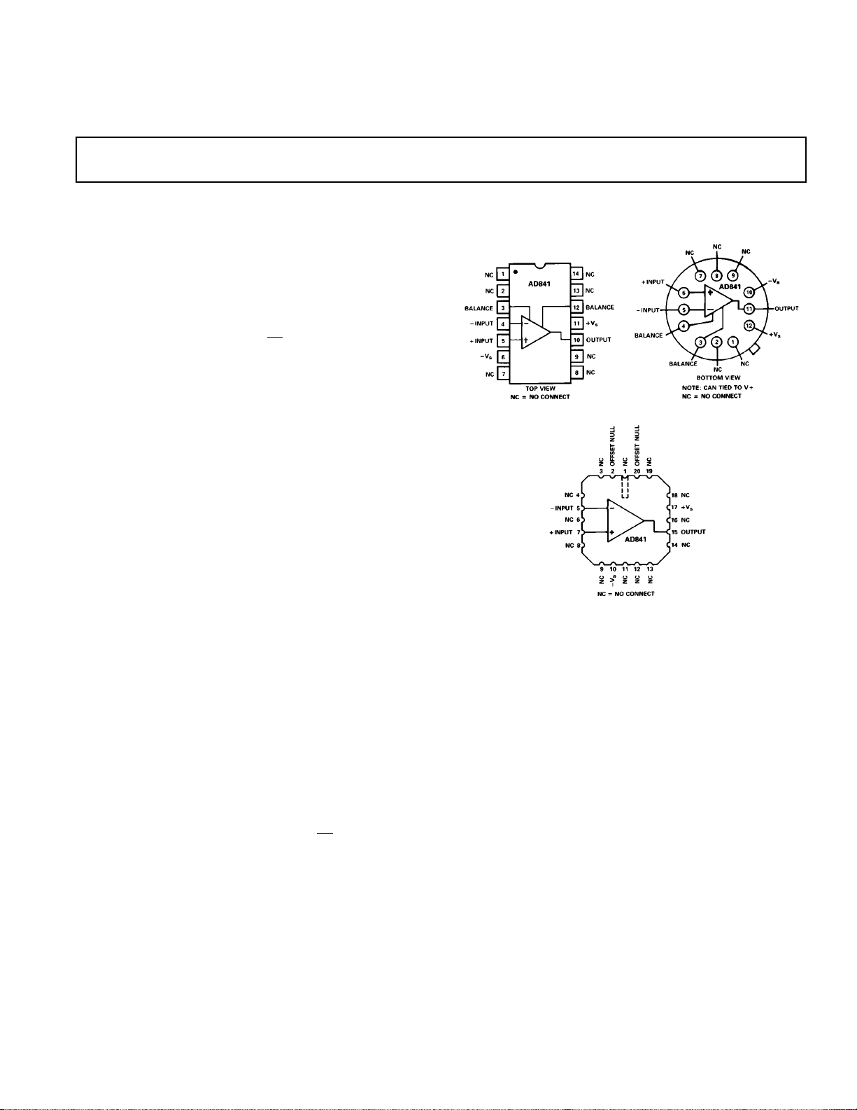
CONNECTION DIAGRAMS
Plastic DIP (N) Package
and
Cerdip (Q) Package
LCC (E) Package
AD841
TO-8 (H) Package
PRODUCT DESCRIPTION
The AD841 is a member of the Analog Devices family of wide
bandwidth operational amplifiers. This high speed/high precision
family includes, among others, the AD840, which is stable at a
gain of 10 or greater, and the AD842, which is stable at a gain of
two or greater and has 100 mA minimum output current drive.
These devices are fabricated using Analog Devices’ junction isolated complementary bipolar (CB) process. This process permits
a combination of dc precision and wideband ac performance
previously unobtainable in a monolithic op amp. In addition to
its 40 MHz unity-gain bandwidth product, the AD841 offers extremely fast settling characteristics, typically settling to within
0.01% of final value in 110 ns for a 10 volt step.
Unlike many high frequency amplifiers, the AD841 requires no
external compensation. It remains stable over its full operating
temperature range. It also offers a low quiescent current of
12 mA maximum, a minimum output current drive capability of
50 mA, a low input voltage noise of 13 nV/√
offset voltage of 1 mV maximum.
The 300 V/µs slew rate of the AD841, along with its 40 MHz
gain bandwidth, ensures excellent performance in video and
pulse amplifier applications. This amplifier is well suited for use
in high frequency signal conditioning circuits and wide bandwidth active filters. The extremely rapid settling time of the
REV. B
Information furnished by Analog Devices is believed to be accurate and
reliable. However, no responsibility is assumed by Analog Devices for its
use, nor for any infringements of patents or other rights of third parties
which may result from its use. No license is granted by implication or
otherwise under any patent or patent rights of Analog Devices.
Hz and low input
AD841 makes it the preferred choice for data acquisition
applications which require 12-bit accuracy. The AD841 is
also appropriate for other applications such as high speed
DAC and ADC buffer amplifiers and other wide bandwidth
circuitry.
APPLICATION HIGHLIGHTS
1. The high slew rate and fast settling time of the AD841
make it ideal for DAC and ADC buffers, and all types
of video instrumentation circuitry.
2. The AD841 is a precision amplifier. It offers accuracy to
0.01% or better and wide bandwidth performance previously available only in hybrids.
3. The AD841’s thermally balanced layout and the speed
of the CB process allow the AD841 to settle to 0.01% in
110 ns without the long “tails” that occur with other
fast op amps.
4. Laser wafer trimming reduces the input offset voltage to
1 mV max on the K grade, thus eliminating the need for
external offset nulling in many applications. Offset null
pins are provided for additional versatility.
5. The AD841 is an enhanced replacement for the
HA2541.
One Technology Way, P.O. Box 9106, Norwood, MA 02062-9106, U.S.A.
Tel: 617/329-4700 Fax: 617/326-8703
Page 2

AD841–SPECIFICATIONS
Model AD841J AD841K AD841S
(@ +258C and 615 V dc, unless otherwise noted)
1
Conditions Min Typ Max Min Typ Max Min Typ Max Units
INPUT OFFSET VOLTAGE
2
T
MIN–TMAX
0.8 2.0 0.5 1.0 0.5 2.0 mV
5.0 3.3 5.5 mV
Offset Drift 35 35 35 µV/°C
INPUT BIAS CURRENT 3.5 8 3.5 5 3.5 8 µA
T
MIN–TMAX
10 612µA
Input Offset Current 0.1 0.4 0.1 0.2 0.1 0.4 µA
T
MIN–TMAX
0.5 0.3 0.6 µA
INPUT CHARACTERISTICS Differential Mode
Input Resistance 200 200 200 kΩ
Input Capacitance 2 2 2 pF
INPUT VOLTAGE RANGE
Common Mode 610 12 610 12 610 12 V
Common-Mode Rejection V
= ±10 V 86 100 103 109 86 110 dB
CM
T
MIN–TMAX
80 100 80 dB
INPUT VOLTAGE NOISE f = 1 kHz 15 15 15 nV/√
Wideband Noise 10 Hz to 10 MHz 47 47 47 µV rms
OPEN-LOOP GAIN V
= ±10 V
O
≥ 500 Ω 25 45 25 45 25 45 V/mV
R
LOAD
T
MIN–TMAX
12 20 12 V/mV
OUTPUT CHARACTERISTICS
Voltage R
Current V
≥ 500 Ω
LOAD
T
MIN–TMAX
= ±10 V 50 50 50 mA
OUT
±10 ±10 ±10 V
OUTPUT RESISTANCE Open Loop 5 5 5 Ω
FREQUENCY RESPONSE
Unity Gain Bandwidth V
Full Power Bandwidth
Rise Time
Overshoot
Slew Rate
4
4
4
3
Settling Time – 10 V Step A
= 90 mV p-p 40 40 40 MHz
OUT
VO = 20 V p-p
≥ 500 Ω 3.1 4.7 3.1 4.7 3.1 4.7 MHz
R
LOAD
AV = –1 10 10 10 ns
AV = –1 10 10 10 %
AV = –1 200 300 200 300 200 300 V/µs
= –1
V
to 0.1% 90 00 90 ns
to 0.01% 110 110 110 ns
OVERDRIVE RECOVERY –Overdrive 200 200 200 ns
+Overdrive 700 700 700 ns
DIFFERENTIAL GAIN f = 4.4 MHz 0.03 0.03 0.03 %
Differential Phase f = 4.4 MHz 0.022 0.022 0.022 Degree
POWER SUPPLY
Rated Performance ±15 ±15 ±15 V
Operating Range ±5 ±18 ±5 ±18 ±5 ±18 V
Quiescent Current 11 12 11 12 11 12 mA
14 14 16 mA
Power Supply Rejection Ratio V
TEMPERATURE RANGE
Rated Performance
5
T
MIN–TMAX
= ±5 V to ±18 V 86 100 90 100 86 100 dB
S
T
MIN–TMAX
80 86 80 dB
0 +75 0 +75 –55 +125 °C
PACKAGE OPTIONS
LCC (E-20A) AD841SE, AD841SE/883B
Cerdip (Q-14) AD841JQ AD841KQ AD841SQ, AD841SQ/883B
Plastic (N-14) AD841JN AD841KN
TO-8 (H-12) AD841JH AD841KH AD841SH, AD841SH/883B
Chips AD841J CHIPS AD841S CHIPS
NOTES
1
Standard Military Drawing Available: 5962-89641012A – (SE/883B); 5962-8964101CA – (SQ/883B).
2
Input offset voltage specifications are guaranteed after 5 minutes at TA = +25°C.
3
Full power bandwidth = Slew Rate/2 π V
3
Refer to Figure 19.
4
“S” grade T
All min and max specifications are guaranteed. Specifications shown in boldface are tested on all production units.
Specifications subject to change without notice.
MIN–TMAX
specifications are tested with automatic test equipment at TA = –55°C and TA = +125°C.
PEAK
.
–2–
REV. B
Hz
Page 3
AD841
ABSOLUTE MAXIMUM RATINGS
Supply Voltage . . . . . . . . . . . . . . . . . . . . . . . . . . . . . . . . ±18 V
Internal Power Dissipation
2
1
TO-8 (H) . . . . . . . . . . . . . . . . . . . . . . . . . . . . . . . . . . 1.4 W
Plastic (N) . . . . . . . . . . . . . . . . . . . . . . . . . . . . . . . . . 1.5 W
Cerdip (Q) . . . . . . . . . . . . . . . . . . . . . . . . . . . . . . . . . 1.3 W
Input Voltage . . . . . . . . . . . . . . . . . . . . . . . . . . . . . . . . . . . ±Vs
Differential Input Voltage . . . . . . . . . . . . . . . . . . . . . . . . ±6 V
Storage Temperature Range
Q, H, E . . . . . . . . . . . . . . . . . . . . . . . . . . –65°C to +150°C
N . . . . . . . . . . . . . . . . . . . . . . . . . . . . . . . .–65°C to +125°C
Junction Temperature . . . . . . . . . . . . . . . . . . . . . . . . . +175°C
Lead Temperature Range (Soldering 60 sec) . . . . . . . . +300°C
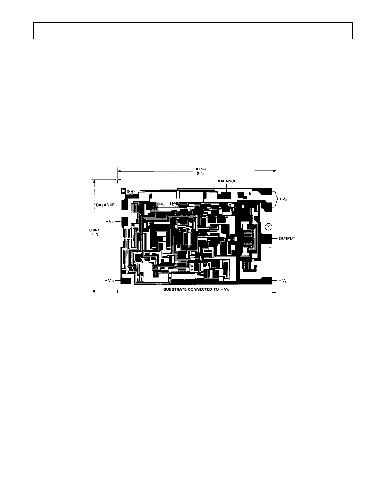
METALIZATION PHOTOGRAPH
Contact factory for latest dimensions.
Dimensions shown in inches and (mm).
NOTES
1
Stresses above those listed under “Absolute Maximum Ratings” may cause
permanent damage to the device. This is a stress rating only, and functional
operation of the device at these or any other conditions above those indicated in
the operational section of this specification is not implied. Exposure to absolute
maximum rating conditions for extended periods may affect device reliability.
2
Maximum internal power dissipation is specified so that TJ does not exceed
+175°C at an ambient temperature of +25°C.
Thermal Characteristics:
Cerdip Package 35°C/W 110°C/W 38°C/W Recommended Heat Sink:
TO-8 Package 30°C/W 100°C/W 37°C/W Aavid Engineering© #602B
Plastic Package 30°C/W 100°C/W
LCC Package 35°C/W 150°C/W
θ
JC
θ
JA
θ
SA
REV. B
–3–
Page 4

AD841–Typical Characteristics
(at +258C and VS = 615 V, unless otherwise noted)
Figure 1. Input Common-Mode
Range vs. Supply Voltage
Figure 4. Quiescent Current vs.
Supply Voltage
Figure 2. Output Voltage Swing
vs. Supply Voltage
Figure 5. Input Bias Current vs.
Temperature
Figure 3. Output Voltage Swing
vs. Load Resistance
Figure 6. Output Impedance vs.
Frequency
Figure 7. Quiescent Current vs.
Temperature
Figure 8. Short-Circuit Current
Limit vs. Temperature
Figure 9. Gain Bandwidth Product
vs. Temperature
REV. B–4–
Page 5

AD841
Figure 10. Open-Loop Gain and
Phase Margin vs. Frequency
Figure 13. Common-Mode
Rejection vs. Frequency
Figure 11. Open-Loop Gain vs.
Supply Voltage
Figure 14. Large Signal Frequency
Response
Figure 12. Power Supply Rejection
vs. Frequency
Figure 15. Output Swing and
Error vs. Settling Time
Figure 16. Harmonic Distortion vs.
Frequency
REV. B
Figure 17. Slew Rate vs.
Temperature
–5–
Figure 18. Input Voltage Noise
Spectral Density
Page 6

AD841
Figure 19a. Inverting Amplifier
Configuration (DIP Pinout)
Figure 20a. Unity-Gain Buffer Amplifier
Configuration (DIP Pinout)
OFFSET NULLING
The input offset voltage of the AD841 is very low for a high
speed op amp, but if additional nulling is required, the circuit
shown in Figure 21 can be used.
Figure 19b. Inverter Large Signal
Pulse Response
Figure 19c. Inverter Small Signal
Pulse Response
Figure 20b. Buffer Large Signal
Pulse Response
INPUT CONSIDERATIONS
An input resistor (RIN in Figure 20) is recommended in circuits
where the input to the AD841 will be subjected to transient or
continuous overload voltages exceeding the ± 6 V maximum differential limit. This resistor provides protection for the input
transistors by limiting the maximum current that can be forced
into the input.
For high performance circuits it is recommended that a resistor
(R
in Figures 19 and 20) be used to reduce bias current errors
B
by matching the impedance at each input. The output voltage
error caused by the offset current is more than an order of magnitude less than the error present if the bias current error is not
removed.
Figure 20c. Buffer Small Signal
Pulse Response
Figure 21. Offset Nulling (DIP Pinout)
AD841 SETTLING TIME
Figures 22 and 24 show the settling performance of the AD841
in the test circuit shown in Figure 23.
Settling time is defined as:
The interval of time from the application of an ideal step
function input until the closed-loop amplifier output has
entered and remains within a specified error band.
This definition encompasses the major components which comprise settling time. They include (1) propagation delay through
the amplifier; (2) slewing time to approach the final output
value; (3) the time of recovery from the overload associated with
slewing and (4) linear settling to within the specified error band.
–6–
REV. B
Page 7

Applying the AD841
Figure 22. AD841 0.01% Settling Time
Expressed in these terms, the measurement of settling time is obviously a challenge and needs to be done accurately to assure the
user that the amplifier is worth consideration for the application.
Figure 23. Settling Time Test Circuit
Measurement of the AD841’s 0.01% settling in 110 ns was accomplished by amplifying the error signal from a false summing
junction with a very high speed proprietary hybrid error amplifier specially designed to enable testing of small settling errors.
The device under test was driving a 500 Ω load. The input to
the error amp is clamped in order to avoid possible problems associated with the overdrive recovery of the oscilloscope input
amplifier. The error amp gains the error from the false summing
junction by 10, and it contains a gain vernier to fine trim the
gain.
Figure 24 shows the “long term” stability of the settling characteristics of the AD841 output after a 10 V step. There is no evidence of settling tails after the initial transient recovery time.
The use of a junction isolated process, together with careful layout, avoids these problems by minimizing the effects of transistor isolation capacitance discharge and thermally induced shifts
in circuit operating points. These problems do not occur even
under high output current conditions.
Figure 24. AD841 Settling Demonstrating No Settling
Tails
GROUNDING AND BYPASSING
In designing practical circuits with the AD841, the user must
remember that whenever high frequencies are involved, some
special precautions are in order. Circuits must be built with
short interconnect leads. Large ground planes should be used
whenever possible to provide a low resistance, low inductance
circuit path, as well as minimizing the effects of high frequency
coupling. Sockets should be avoided because the increased
interlead capacitance can degrade bandwidth.
Feedback resistors should be of low enough value to assure that
the time constant formed with the circuit capacitances will not
limit the amplifier performance. Resistor values of less than
5 kΩ are recommended. If a larger resistor must be used, a
small (<10 pF) feedback capacitor in parallel with the feedback
resistor, R
tances and optimize the dynamic performance of the amplifier
in the particular application.
Power supply leads should be bypassed to ground as close as
possible to the amplifier pins. A 2.2 µF capacitor in parallel
with a 0.1 µF ceramic disk capacitor is recommended.
CAPACITIVE LOAD DRIVING ABILITY
Like all wideband amplifiers, the AD841 is sensitive to capacitive loading. The AD841 is designed to drive capacitive loads of
up to 20 pF without degradation of its rated performance. Capacitive loads of greater than 20 pF will decrease the dynamic
performance of the part although instability should not occur
unless the load exceeds 100 pF (for a unity-gain follower). A
resistor in series with the output can be used to decouple larger
capacitive loads.
Figure 25 shows a typical configuration for driving a large capacitive load. The 51 Ω output resistor effectively isolates the
high frequency feedback from the load and stabilizes the circuit.
Low frequency feedback is returned to the amplifier summing
junction via the low pass filter formed by the 51 Ω resistor and
the load capacitance, C
, may be used to compensate for these stray capaci-
F
.
L
REV. B
–7–
Page 8

AD841
Figure 25. Circuit for Driving a Large Capacitive Load
USING A HEAT SINK
The AD841 draws less quiescent power than most precision
high speed amplifiers and is specified for operation without a
heat sink. However, when driving low impedance loads, the current to the load can be 4 to 5 times the quiescent current. This
will create a noticeable temperature rise. Improved performance
can be achieved by using a small heat sink such as the Aavid
Engineering #602B.
TERMINATED LINE DRIVER
The AD841 functions very well as a high speed line driver of either terminated or unterminated cables. Figure 26 shows the
AD841 driving a doubly terminated cable in a follower configuration. The AD841 maintains a typical slew rate of 300 V/µs,
which means it can drive a ±10 V, 4.7 MHz signal or a ±3 V,
15.9 MHz signal.
The termination resistor, R
, (when equal to the characteristic
T
impedance of the cable) minimizes reflections from the far end
of the cable. A back-termination resistor (R
, also equal to the
BT
characteristic impedance of the cable) may be placed between
the AD841 output and the cable in order to damp any stray signals caused by a mismatch between R
and the cable’s charac-
T
teristic impedance. This will result in a “cleaner” signal, but
since 1/2 the output voltage will be dropped across R
, the op
BT
amp must supply double the output signal required if there is no
back termination. Therefore the full power bandwidth is cut in
half.
If termination is not used, cables appear as capacitive loads. If
this capacitive load is large, it should be decoupled from the
AD841 by a resistor in series with the output (see above:
Driving a Capacitive Load).
Figure 27. Overdrive Recovery
Figure 28. Overdrive Recovery Test Circuit
OUTLINE DIMENSIONS
Dimensions shown in inches and (mm).
14-Pin Cerdip (Q) Package14-Pin Plastic (N) Package
12-Lead Metal Can Package
(TO-8 Style)
20-Terminal Leadless
Ceramic Chip Carrier
C1242–15–11/88
E-20A
Figure 26. Line Driver Configuration
OVERDRIVE RECOVERY
Figure 27 shows the overdrive recovery capability of the AD841.
Typical recovery time is 200 ns from negative overdrive and
700 ns from positive overdrive.
–8–
PRINTED IN U.S.A.
REV. B
 Loading...