

Page 1
REV. 0
Information furnished by Analog Devices is believed to be accurate and
reliable. However, no responsibility is assumed by Analog Devices for its
use, nor for any infringements of patents or other rights of third parties
which may result from its use. No license is granted by implication or
otherwise under any patent or patent rights of Analog Devices.
a
8-Bit, 4-Channel Data
Acquisition System
AD8401
One Technology Way, P.O. Box 9106, Norwood, MA 02062-9106, U.S.A.
Tel: 617/329-4700 Fax: 617/326-8703
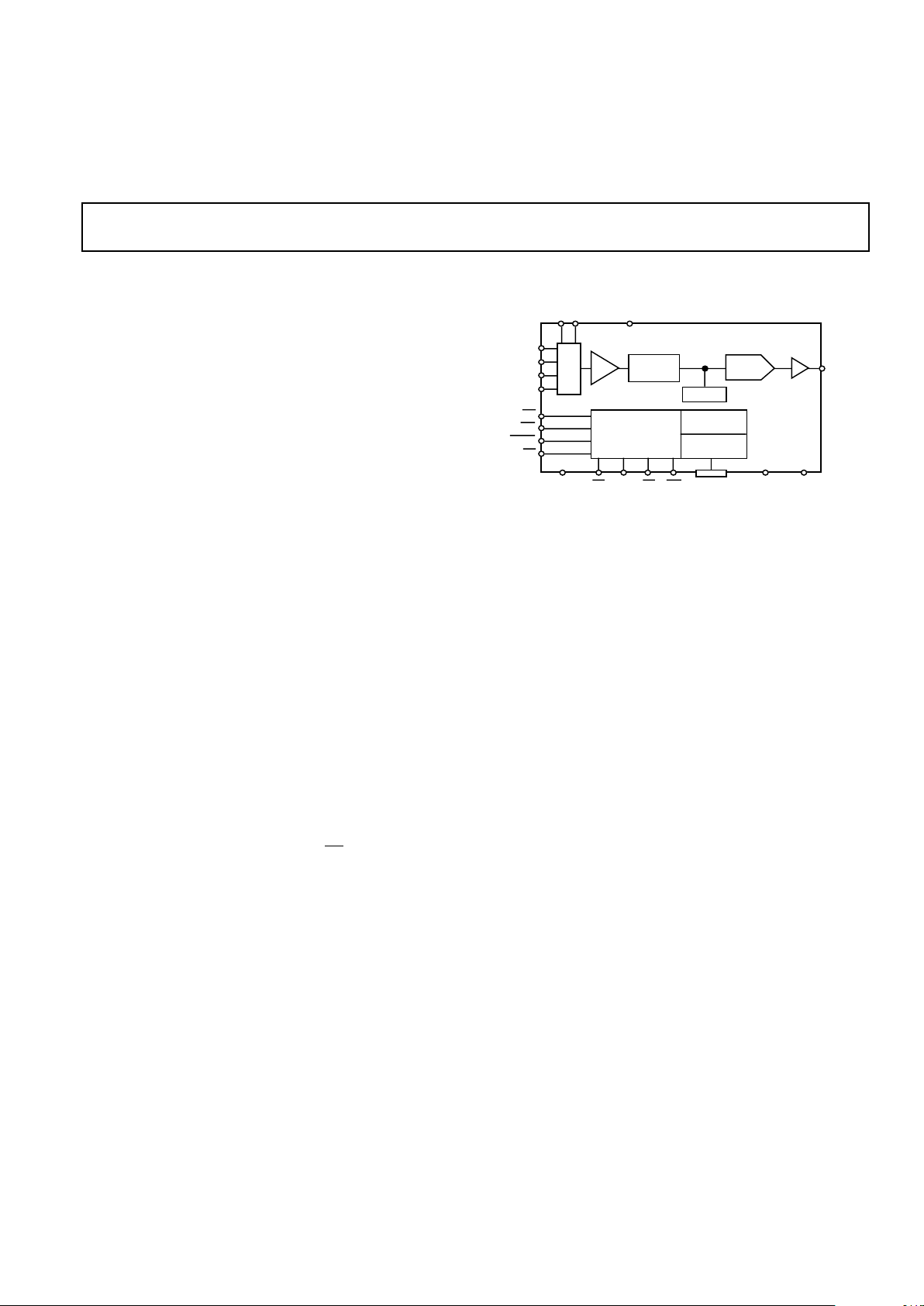
FUNCTIONAL BLOCK DIAGRAM
V
OUT
DGND
AG
DACAGADC
DATA I/O
(8 BITS)
M
U
X
T/H
8-BIT ADC
1.25 REF
8-BIT
DAC
RS
INT
BUSY
ST
DAC REG
ADC REG
CONTROL LOGIC
A0 A1
VDD (+5.0V)
RD WRCLK CS
AD8401
V
A
IN
V
B
IN
V
C
IN
V
D
IN
FEATURES
2 ms ADC with T/H
4-Channel MUX
AD899 Compatible
+5 Volt Operation
On-Chip Reference
4 ms Voltage Output DAC
Fast Bus Access Time—75 ns
APPLICATIONS
Servo Controls
Digitally Controlled Calibration
Process Control Equipment
GENERAL DESCRIPTION
The AD8401 is a complete data acquisition and control system
containing ADC, DAC, 4-channel MUX, and internal voltage
reference. Built using CBCMOS, this monolithic circuit offers
the user a complete system with very high package density and
reliability.
The converter is a successive approximation ADC with T/H,
and is capable of operating with conversion times as short as
2 µs. Analog input bandwidth is 200 kHz, and DAC output volt-
age settling time is less than 4 µs, making the AD8401 capable
of controlling servo loops with speed and precision.
The 8-bit data interface provides both read and write operation
for parallel bus interfaces to microcontrollers and DSP processors. An external 5 MHz clock sets the 2 µs conversion rate.
Slower clocks reduce the conversion time and the internal power
dissipation. The standard control lines: Reset, Busy, Interrupt,
Read and Write complete the handshaking signals for microprocessor communication. A start trigger
ST input allows pre-
cise sampling intervals in synchronous sampling applications.
The input multiplexer addressing is designed for direct interface
to the AD899 hard-disk drive, read-channel device with no extra
hardware or special software. Analog input range levels are likewise compatible with the AD899.
The AD8401 is designed to operate from a single +5 volt supply, which will give an ADC input range of 0 V to 3.0 V, and
DAC output range of 0 V to 2.5 V.
The AD8401 is offered in the SOIC-28 surface mount package,
and is guaranteed to operate over the extended industrial temperature range of –40°C to +85°C.
Page 2
Parameter Symbol Conditions Min Typ Max Units
STATIC PERFORMANCE
Resolution N 8 Bits
Total Unadjusted Error TUE ±3 LSB
Relative Accuracy INL –1 +1 LSB
Differential Nonlinearity DNL –1 +1 LSB
Offset Error V
OSE
TA = +25°C –4 +4 LSB
T
A
= Full Temp Range –6 +6 LSB
Full-Scale Error A
E
TA = +25°C –4 +4 LSB
T
A
= Full Temp Range –6 +6 LSB
∆Full-Scale/∆V
DD
TA = +25°C 1 LSB
DYNAMIC PERFORMANCE
Signal-to-Noise Ratio SNR 44 dB
Total Harmonic Distortion THD 48 dB
Intermodulation Distortion IMD 60 dB
Frequency Response 0 to 200 kHz 0.1 dB
Track/Hold Acquisition Time t
AQ
200 ns
ANALOG INPUTS (Applies to Inputs A, B. C, D)
Unipolar Input Range V
IN
03V
Input Current I
IN
–500 +500 µA
Input Capacitance C
IN
10 pF
LOGIC INPUTS
Clock Input Current Low I
CKL
VIN = 0 V 1.6 mA
Clock Input Current High I
CKH
VIN = V
DD
40 µA
Input Leakage Current I
L
CS, RD, RS, ST 10 µA
LOGIC OUTPUTS (Applies to Outputs DB0–DB7,
INT, BUSY)
Logic Output Low Voltage V
OL
IOL = 1.6 mA 0.4 V
Logic Output High Voltage V
OH
IOH = 200 µA 4.0 V
Output Leakage Current I
OZ
CS = 1 (Except INT & BUSY)10µA
Output Capacitance C
OZ
CS = 1 (Except INT & BUSY)10pF
CONVERSION TIME t
C
External Clock 2 µs
Specifications subject to change without notice.
REV. 0
–2–
AD8401–SPECIFICA TIONS
ADC ELECTRICAL CHARACTERISTICS
A1 A0 Input Selected
00V
IN
A
01V
IN
B
10V
IN
C
11V
IN
D
Table I. Multiplexer Address Input Decode
(@ VDD = +5.0 V 6 5%, AG
DAC
= AG
ADC
= 0.0 V; f
CLK
= 5 MHz; –408C ≤ TA ≤ +858C,
unless otherwise noted)
Page 3

DAC ELECTRICAL CHARACTERISTICS
Parameter Symbol Conditions Min Typ Max Units
STATIC PERFORMANCE
Resolution N 8 Bits
Total Unadjusted Error TUE ±2 LSB
Relative Accuracy INL –1 +1 LSB
Differential Nonlinearity DNL –1 +1 LSB
Offset Error V
OSE
TA = +25°C –2 +2 LSB
T
A
= Full Temp Range –2.5 +2.5 LSB
Full-Scale Error A
E
TA = +25°C –3 +3 LSB
T
A
= Full Temp Range –4 +4 LSB
∆Full-Scale/∆V
DD
TA = +25°C –0.5 +0.5 LSB
Load Regulation at Full-Scale –0.2 +0.2 LSB
DYNAMIC PERFORMANCE
Signal-to-Noise Ratio SNR 44 dB
Total Harmonic Distortion THD 48 dB
ANALOG OUTPUT
Output Voltage Range OVR 0 +2.5 V
LOGIC INPUTS (Applies to DB0–DB7, CS, WR, RD, RS)
Logic Input Low Voltage V
IL
0.8 V
Logic Input High Voltage V
IH
2.4 V
Input Leakage Current I
L
–10 10 µA
Input Capacitance C
IL
10 pF
AC CHARACTERISTICS
Voltage Output Settling Time t
S
To ±1/2 LSB of Final Value 2 4 µs
Positive Full-Scale Change t
POS
10% to 90% 1 2 µs
Negative Full-Scale Change t
NEG
90% to 10% 2 4 µs
DAC Glitch Impulse 15 nV s
Digital Feedthrough 1 nV s
VIN to V
OUT
Isolation f = 50 kHz 60 dB
POWER REQUIREMENTS
Positive Supply Current I
DD
No Load 13 mA
Specifications subject to change without notice.
(@ VDD = +5.0 V 6 5%, AG
DAC
= AG
ADC
= 0.0 V; RL = 2 kV, CL = 100 pF
to AG
DAC
; –408C ≤ TA ≤ +858C, unless otherwise noted)
AD8401
–3–
REV. 0
Page 4
AD8401
–4–
REV. 0
WARNING!
ESD SENSITIVE DEVICE
CAUTION
ESD (electrostatic discharge) sensitive device. Electrostatic charges as high as 4000 V readily
accumulate on the human body and test equipment and can discharge without detection.
Although the AD8401 features proprietary ESD protection circuitry, permanent damage may
occur on devices subjected to high energy electrostatic discharges. Therefore, proper ESD
precautions are recommended to avoid performance degradation or loss of functionality.
TIMING ELECTRICAL SPECIFICATIONS
(@ VDD = +5.0 V 6 5%, AG
DAC
= AG
ADC
= 0.0 V; f
CLK
= 5 MHz; –408C ≤ TA ≤ +858C,
unless otherwise noted)
Parameters
1, 2, 3
Symbol Condition Min Typ Max Units
DAC TIMING (See Figure 8 Timing Diagram)
WR Pulse Width t
1
50 ns
CS to WR Setup Time t
2
0ns
CS to WR Hold Time t
3
0ns
Data Setup Time t
4
60 ns
Data Hold Time t
5
0ns
ADC TIMING (See Figures 6 and 7 Timing Diagrams)
ST Pulse Width t
6
40 ns
ST to BUSY Delay t
7
110 ns
BUSY to INT Delay t
8
30 ns
BUSY to CS Delay t
9
0ns
CS to RD Setup Time t
10
0ns
RD Pulse Width
4
t
11
75 ns
CS to RD Hold Time t
12
0ns
Data Access after
RD t
13
CL = 20 pF 10 75 ns
Data Access after
RD t
13
CL = 100 pF 10 135 ns
Bus Relinquish after
RD t
14
10 70 ns
RD to INT Delay t
15
85 ns
RD to BUSY Delay t
16
110 ns
Data Valid after
BUSY t
17
CL = 20 pF 90 ns
Data Valid after BUSY t
17
CL = 100 pF 135 ns
NOTES
1
All input control signals are specified with tR = tF = 5 ns (10% to 90% of +5 V) and timed from a voltage level of 1.6 V.
2
t13 and t17 are measured with the load circuits of Figure 1 and defined as the time required for an output to cross either 0.8 V or 2.4 V.
3
t14 is defined as the time required for the data line to change 0.5 V when loaded with the circuit of Figure 2.
4
t15 is determined by t13.
ABSOLUTE MAXIMUM RATINGS*
Supply Voltage (VDD) . . . . . . . . . . . . . . . . . . . . . . . . . . . +8 V
Input Voltages . . . . . . . . . . . . . . . . . . . –0.3 V to V
DD
+ 0.3 V
Output Short-Circuit Duration . . . . . . . . . . . . . . . . Indefinite
Package Power Dissipation . . . . . . . . . . . . . . (T
J
max–TA)/θ
JA
Thermal Resistance θ
JA
28-Lead SOIC (R) . . . . . . . . . . . . . . . . . . . . . . . . . 53°C/W
Storage Temperature Range . . . . . . . . . . . . –65°C to +150°C
Operating Temperature Range . . . . . . . . . . . . –40°C to +85°C
Junction Temperature Range (T
J
max) . . . . –65°C to +150°C
Lead Temperature Range (Soldering, 60 sec) . . . . . . +300°C
*Stresses above those listed under “Absolute Maximum Ratings” may cause
permanent damage to the device. This is a stress rating only and functional
operation of the device at these or any other conditions above those indicated in the
operational sections of this specification is not implied. Exposure to absolute
maximum rating conditions for extended periods may affect device reliability.
ORDERING GUIDE
Temperature Package Package
Model* Range Description Option
AD8401AR –40°C to +85°C 28-Lead SOIC SOL-28
AD8401Chips +25°C Die
*The AD8401 contains 1257 transistors.
Figure 1. Load Circuits for Data Access Time Test
a. V
OH
to High Z
a. High Z to V
OH
b. High Z to V
OL
DGND
CL
3kΩ
DBN
DBN
CL
3kΩ
+5V
DGND
DGND
10pF
3kΩ
DBN
DBN
10pF
3kΩ
+5V
DGND
b. VOL to High Z
Figure 2. Load Circuits for Bus Relinquish Time Test
Page 5

AD8401
–5–
REV. 0
PIN DESCRIPTIONS
Pin# Name Description
1V
DD
Positive Supply. Nominal value +5 volts. This pad requires 2 bonds for die assembly.
The substrate is common with V
DD
.
2AG
DAC
Analog Ground for the DAC. There is a separate analog ground for the ADC.
3V
OUT
Voltage Output from the DAC.
4 NC No Connect.
5 A1 Address Input that controls multiplexer. See Table I for address decode.
6 RESET (
RS) Active Low Digital Input that clears the DAC register to zero, setting the DAC to mini-
mum scale. It also asynchronously clears the
INT line of the ADC.
7–12, 14, 15 DB7 to DB0 Digital I/O Lines. DB7 (7) is the Most Significant Bit (MSB), for both the ADC and
the DAC, and DB0 (15) is the Least Significant Bit (LSB).
13 DGND Digital Ground.
16
WR Rising Edge Triggered Write Input. Used to load data into the DAC register.
17
CS Chip Select. Active Low Input
18
RD Active Low Read Input. When this input is active, ADC data can be read from the
part.
RD going low starts the ADC conversion.
19
ST Falling Edge Triggered Start Input. Used for applications requiring precise sample tim-
ing. The falling edge of
ST starts the conversion and sets the BUSY low. The ST is not
gated by
CS.
20
BUSY ADC Active Low, Status Output. When the ADC is performing a conversion, the
BUSY output is low.
21
INT Active Low Output. The Interrupt output notifies the system that the ADC has com-
pleted its conversion.
INT goes high on the rising edge of CS or RD. It will also be
forced high when RESET is asserted.
22 CLK External Clock Input Pin. Accepts a TTL or 5 V CMOS input logic levels.
23 AG
ADC
Analog ADC Ground
27–24 V
IN
A, B, C, D Four Analog Inputs
28 A0 Address input that controls multiplexer. See Table I for address decode.
PIN CONFIGURATION
Top View
(Not to Scale)
1
2
3
7
8
9
10
11
12
4
5
6
13
14
28
27
26
22
21
20
19
18
17
25
24
23
16
15
AD8401AR
V
DD
AG
DAC
V
OUT
NC
A1
DB7
DB6
DB5
DB4
DB3
DB2
DGND
DB1
A0
VINA
VINB
VINC
VIND
AG
ADC
CLK
DB0
BUSY
INT
ST
RD
CS
WR
RS
NC = NO CONNECT
DICE CHARACTERISTICS
1
23
5
6
7
8
9
10
11 12 13 14 15 16 17
18
19
20
21
22
23
24
25
2627
Die Size 91 X 121 mil = 11,011 sq mil
28
Page 6

AD8401
–6–
REV. 0
OPERATION
The AD8401 is a complete data acquisition and control system.
It contains the DAC, a four channel input multiplexer, a track/
hold, an ADC, as well as an internal bandgap reference. It interfaces to the microcontroller via an 8-bit digital I/O port.
D/A CONVERTER SECTION
The DAC is an 8-bit voltage mode DAC with an output that
swings from AG
DAC
to the 1.25 volt bandgap voltage. It uses an
R-2R ladder fed by PNP current sources which allow the output
to swing to ground so that the DAC operates in a unipolar mode.
AMPLIFIER SECTION
The DAC’s output is buffered by an internal high speed op
amp. The op amps output range is set at 0 V to 2.5 V. The op
amp has a 500 ns typical settling time to 0.2% for positive
slewing signals. There are differences in settling time for negative slewing signals. Signals going to zero volts will settle slightly
slower to ground than is seen in the positive direction.
20Ω
20Ω
V
OUT
V
DD
AG
DAC
n-CH
Figure 3. Equivalent Amplifier Output Stage
Current sinking capability is also limited near zero volts in single
supply operation. Figure 3 provides an equivalent amplifier output stage schematic.
INTERNAL REFERENCE
An on-chip bandgap is provided as a voltage reference to both
the DAC and the ADC. This reference is internal to the
AD8401 and is not accessible to the user. It is laser trimmed for
both absolute accuracy and temperature coefficients. The reference is internally buffered by a separate control amplifier for both
the DAC and ADC to improve isolation between the converters.
DIGITAL I/O
The 8-bit parallel data I/O port on the AD8401 provides access
to both the DAC and the ADC. This port is TTL/CMOS compatible with three-state outputs that are ESD protected.
The data format is binary. This data coding applies to both the
DAC and the ADC. See the applications information section.
ADC SECTION
A fast successive approximation ADC is used to attain a conversion time of 2 microseconds. Start of conversion is initiated by
CS and RD. Following a Start command the BUSY signal will
become active and another Start command should not be given
until the conversion is complete.
The RESET (
RS) input does not affect A/D conversion, but the
INT (Interrupt or conversion complete) which normally goes
active low at the end of a conversion will be forced high by
RESET asynchronously.
Figure 4 shows the wave forms for a conversion cycle. The track
and hold begins holding the input voltage V
IN
approximately
50 ns after the falling edge of the Start command. The MSB decision is made approximately 50 ns after the second falling edge
of the CLK. If t
X
is greater than 50 ns, then the falling edge of
the CLK will be seen as the first falling clock edge. If t
X
is less
than 50 ns, the first MSB conversion will not occur until one
clock cycle later. The following bits will each be converted in a
similar manner 50 ns after each CLK edge until all eight bits
have been converted. After the end of conversion the contents of
the ADC SAR register are transferred to the output data latch,
the track and hold is returned to the track mode,
INT goes low
and the SAR is reset.
V
IN
CLK
BUSY
CS , RD
OR ST
100ns
TYP
50ns TYP
MSB DECISION
DB7
LSB DECISION
DB0
t
x
50ns TYP
Figure 4. Operating Waveforms Using the External Clock
ANALOG INPUT
The analog inputs of the AD8401 are fed into resistor voltage
divider networks with a typical value of 8.5 kΩ. The amplifiers
driving these inputs must have an output resistance low enough
to drive these nodes without losing accuracy. Taps from the
voltage dividers are connected to the track and hold amplifier by
the multiplexer switches.
T/H
VIND
V
IN
A
5kΩ
MUX
AGADC
5kΩ
3.57kΩ
3.57kΩ
Figure 5. Equivalent Analog Input Circuit
TRACK-AND-HOLD AMPLIFIER
Following the resistive divider at the input of the AD8401 is a
track-and-hold amplifier that captures input signals accurately
up to the 200 kHz Nyquist frequency of the ADC. To attain this
performance the T/H amplifier must have a much greater bandwidth than the signal of interest. Because of this the user must
be careful to band limit the input signal to avoid aliasing high
frequency components and noise into the passband.
The track-and-hold amplifier is internally controlled by the Start
command and is not directly available to the user. After the
Start command signal the track-and-hold is placed into the hold
mode; it returns to the track mode after the conversion is
complete.
Page 7

AD8401
–7–
REV. 0
BUSY
t
10
INT
t
16
t
15
CS
t
14
t
8
t
17
RD
DATA NEW DATA
HIGH Z
OLD DATA
t
12
t
11
t
9
t
13
Figure 7. Mode 2, ADC Interface Timing
Mode 2 Interface
This interface mode can be used with microprocessors that can
be put into a WAIT state for at least 2 microseconds. The
ST
pin must be tied to logic high for proper operation. The microprocessor begins a conversion by executing a READ instruction
that asserts the
CS and RD pins at the AD8401’s decoded ad-
dress. The AD8401
BUSY output then goes low, forcing the
microprocessor’s READY (or WAIT) line into a WAIT state.
The analog input signal is captured by the T/H on the falling
edge of
RD. When the conversion is complete (8 clocks later),
the
BUSY line returns high, and then the µP completes its
READ of the new data now on the digital output port of the
AD8401. Note that while conversion is in progress the ADC
places the results from the last conversion (Old Data) on the
data bus. The Figure 7 timing diagram details the applicable
timing specification requirements.
DIGITAL INTERFACE: DAC TIMING AND CONTROL
Table II shows the truth table for DAC operation. The internal
8-bit DAC register contents are loaded from the data bus when
both
WR and CS are asserted. The DAC register determines the
D/A converter analog-output voltage. The
WR input is a positive edge triggered input that loads the bus data into the DAC
register subject to the data setup and data hold timing requirements. When
CS and WR are low, the DAC register contents
will not change with changing data bus values. Figure 8 provides
the detail timing diagram for write cycle operation.
Table II. DAC Register Logic
CS WR RS DAC Function
H H H No Effect
L L H No Effect
L ` H DAC Register Updated
` L H DAC Register Updated
X X L DAC Register Loaded with all Zeros
t
2
CS
t
5
WR
DATA VALID DATA
t
3
t
1
t
4
Figure 8. Write Cycle Timing
CLOCK
The AD8401 uses an external clock that is TTL or 5 V CMOS
compatible. The external clock speed is 5 MHz and the duty
cycle may vary from 30% to 70%. The external clock can be
continuously operated between conversions.
DIGITAL INTERFACE: ADC TIMING AND CONTROL
Two basic ADC operating modes are available with the
AD8401. The first mode uses the Start (
ST) pin to trigger a
synchronized A/D conversion. As soon as the
ST pin is asserted,
the T/H switches from tracking to the hold mode capturing the
present analog input-voltage sample. With the T/H holding the
analog sample the successive-approximation analog-to-digital
conversion is completed on that sample value. At the end of
conversion the T/H returns to the tracking mode. This mode of
conversion is ideal for digital signal processing applications
where precise interval sampling is necessary to minimize errors
due to sampling uncertainty or jitter. A precise clock source can
be used to drive the
ST input.
The second mode of conversion is started by the
RD and CS in-
puts going low, after which the
BUSY line puts the microprocessor into a WAIT state until end of conversion. Mode 2 is
asserted by connecting the
ST pin to logic high. The major advantage of this interface is that a single Read Instruction will
start and complete a new analog-to-digital conversion without
the need for carefully tailored software delays that often are not
portable when software routines are taken to a different processor running at a different clock speed.
BUSY
ST
t
6
t
7
t
CONVERT
t
8
INT
t
9
t
15
t
12
CS
t
14
t
11
t
10
t
13
RD
DATA
DATA VALIDHIGH Z
Figure 6. Mode 1, ADC Interface Timing
Mode 1 Interface
As shown in Figure 6, the falling edge of the ST pulse initiates a
conversion and puts the T/H amplifier into the hold mode. The
BUSY signal goes low during the whole A/D conversion time
and returns high signaling end of conversion. The
INT line can
be used to interrupt the microprocessor. When the microprocessor performs a READ to access the AD8401 data, the rising
edges of
CS or RD will reset the INT output to high after the t
15
timing specification. INT can also be used to externally trigger a
pulse that activates the
CS and RD and places the new data into
a buffer or First In First Out FIFO memory. The microprocessor can then load a series of readings from this buffer memory at
a convenient time. Care must be taken not to have the
ST input
high when
RD is brought low; otherwise, the AD8401 will not
operate properly. Also triggering the
ST line a second time be-
fore conversion is complete will cause erroneous readings.
Page 8

AD8401
–8–
REV. 0
An active low pulse, at any time, on the RESET pin asynchronously forces all DAC register bits to zero. The DAC output
voltage becomes zero volts and stays at that value until a new
data word is loaded into the DAC register with a new
WR command. The equivalent input logic for the DAC register loading
is shown in Figure 9.
RESET
CS
WR
DAC REGISTER
D0 D7
INPUT DATA
TO DAC LADDER
Figure 9. Equivalent DAC Register Control Logic
TYPICAL PERFORMANCE CHARACTERISTICS
1.0
–0.1
256
–0.5
0
0
0.5
19212864
DIGITAL INPUT CODE – DECIMAL
VDD = +5V
T
A
= +25°C
LINEARITY ERROR – LSB
Figure 10. ADC Linearity Error vs. Digital Code
1.0
–0.1
256
–0.5
0
0
0.5
19212864
DIGITAL INPUT CODE – DECIMAL
VDD = +5V
T
A
= +25°C
LINEARITY ERROR – LSB
Figure 11. DAC Linearity Error vs. Digital Code
120
0
4.5
30
10
–3.5
20
–4.5
60
40
50
70
80
90
110
100
3.52.51.50.5–0.5–1.5–2.5
FULL SCALE ERROR – LSB
UNITS
SS = 300 UNITS TA = +25°C
Figure 12. ADC Full-Scale Error Histogram
2.5
–3.0
–1.5
–2.5
–2.0
0
–1.0
–0.5
0.5
1.0
1.5
2.0
100–25–50 7550250
TEMPERATURE – °C
ADC FULL-SCALE ERROR – LSB
VDD = +5V
Figure 13. ADC Full-Scale Error vs. Temperature
Page 9

AD8401
–9–
REV. 0
TA = +25°C
SS = 300 UNITS
–3–4 43210–1–2
FULL SCALE ERROR – LSB
0
240
60
20
40
120
80
100
140
160
180
220
200
UNITS
Figure 14. DAC Full-Scale Error Histogram
3.0
–2.5
–1.0
–2.0
–1.5
0.5
–0.5
0
1.0
1.5
2.0
2.5
DAC FULL SCALE ERROR – LSB
100–25–50 7550250
TEMPERATURE – °C
VDD = +5V
x +3σ
x – 3σ
x
Figure 15. DAC Full-Scale Error vs. Temperature
5001000 400300200
BURN-IN TIME @ 150°C – HOURS
4
–5
–3
–4
–2
–1
0
1
2
3
DAC FULL SCALE OUT CHANGE – LSB
VDD = +5V
SS = 135 UNITS
x – 3σ
x
x +3σ
Figure 16. DAC Full-Scale Out Change vs Time
Accelerated by Burn-In
VDD = +5V
T
A
= +25°C
RL TO V
DD
RL TO GND
100 10k1k 100k10
LOAD RESISTANCE – Ω
2.5
1.0
0
0.5
1.5
2.0
OUTPUT VOLTAGE – Volts
Figure 17. DAC Output Swing vs. Load Resistance
10
90
100
0%
1V
5V
1µS5V
3
2
1
0
5V
0
5V
0
5V
0
V
OUT
DATA
WR
TIME – 1µs/DIV
Figure 18. DAC Output Slew Rate Positive Transition
10
90
100
0%
1V
5V
1µS5V
3
2
1
0
5V
0
0
5V
0
V
OUT
DATA
WR
TIME – 1µs/DIV
Figure 19. DAC Output Slew Rate Negative Transition
Page 10

AD8401
–10–
REV. 0
100–25–50 7550250
TEMPERATURE – °C
10.0
6.0
7.0
6.5
8.0
7.5
8.5
9.0
9.5
SUPPLY CURRENT – mA
VIN = +2.4V
VDD = +5.25V
VDD = +4.75V
Figure 21. Supply Current vs. Temperature
10
90
100
0%
500mV
20µS
TIME – 20µs /DIV
VDD = +5V
TA = +25°C
CL = 1000pF
V
OUT
– 0.5V /DIV
Figure 20. DAC Output Swing with Capacitive Load
1k 10k 1M100k
FREQUENCY – Hz
20
0
40
60
POWER SUPPLY REJECTION – dB
TA = +25°C
OUTPUT = FULL SCALE
V
DD
= 5V ± 200mV
Figure 22. Power Supply Rejection Ratio vs. Frequency
Page 11

AD8401
–11–
REV. 0
Table III. DAC Unipolar Code
Nominal
Analog
DAC Register Contents General Transfer
Decimal Binary Equation Output V
OUT
255 1111 1111
2.500×
255
256
2.490 V
129 1000 0001
2.500×
129
256
1.260 V
128 1000 0000
2.500×
128
256
1.250 V
127 0111 1111
2.500×
127
256
1.240 V
1 0000 0001
2.500×
1
256
0.010 V
0 0000 0000
2.500×
0
256
0.000 V
APPLICATIONS INFORMATION
The software programming needs to format data as defined by
the transfer equations and Code Tables that follow.
DAC Transfer Equation
V
OUT
=2.500 ×
D
256
=2.500 ×
255
256
for a 2.50 V full scale
where D is the decimal value 0 through 255 of the 8-bit data
word.
The nominal output voltages listed in the Code Table are subject to the static performance specifications. The INL, ZeroScale and Full-Scale errors describe the total specified variation
that will be encountered from part to part. One LSB of error for
the 2.5 V FS range is 9.766 millivolts (= 2.50/256).
Although separate AGNDs exist for both the DAC and ADC to
minimize crosstalk, writing data to the DAC while the ADC is
performing a conversion may result in an incorrect conversion
from the ADC due to signal interaction between the DAC and
ADC. Therefore, to ensure correct operation of the ADC, the
DAC register should not be updated while the ADC is converting.
The AD8401 is configured for an input range of +3.0 volts Full
Scale. The nominal transfer characteristic for this range is plotted in Figure 23. The output coding is natural binary with one
LSB equal to 11.72 millivolts. Note that the first code transition
between 0 LSB and 1 LSB occurs at 5.8 mV, one half of the
11.72 mV LSB step size. The last code transition occurs at Full
Scale minus 1.5 LSBs, which is a 2.982 V input.
The AD8401 is easily interfaced to most microprocessors by using either address bits or address decode to select the appropriate multiplexer channel. Figure 24 shows how easily the AD8401
interfaces to the AD899. No additional hardware is required.
OUTPUT
CODE
FULL SCALE
TRANSITION
123 FS
FS – 1LSB
V
IN
INPUT VOLTAGE – LSBs
1LSB = FS
256
11111111
11111110
11111101
00000011
00000010
00000001
00000000
Figure 23. ADC 0 V to +3 V Input Transfer Characteristic
Page 12

AD8401
–12–
REV. 0
C1857–18–10/93
PRINTED IN U.S.A.
28-Lead Wide-Body SO
(SOL-28)
SEATING
PLANE
0.0118 (0.30)
0.0040 (0.10)
0.0192 (0.49)
0.0138 (0.35)
0.1043 (2.65)
0.0926 (2.35)
0.0500
(1.27)
BSC
0.0125 (0.32)
0.0091 (0.23)
0.0500 (1.27)
0.0157 (0.40)
8°
0°
0.0291 (0.74)
0.0098 (0.25)
x 45°
0.7125 (18.10)
0.6969 (17.70)
0.4193 (10.65)
0.3937 (10.00)
0.2992 (7.60)
0.2914 (7.40)
PIN 1
28 15
141
OUTLINE DIMENSIONS
Dimensions shown in inches and (mm).
VDD (+5.0V)
1.25V REF
8-BIT DAC
V
OUT
CONTROL LOGIC
DAC REG
ADC REG
8-BIT ADC
ADDRESS BUS
T/H
AD899
A
B
C
D
A1 A0
AG
ADC
AG
DAC
DATA I/O
(8 BITS)
A0
A1
VINA
VINB
VINC
VIND
DGND
RESET
INT
BUSY
ST
CLOCK
WR
CS
RD
AD8401
Figure 24. AD8401 Interface to the AD899 Read-Channel Hard Disk Drive Circuit
 Loading...