

Page 1
Low Power, High Output Current,
V
Dual-Port ADSL/ADSL2+ Line Driver
FEATURES
2 differential DSL channels comprised of current feedback,
high output current amplifiers
Integrated feedback and gain resistors
Integrated biasing network
Ideal for use as ADSL/ADSL2+ dual-channel Central Office
(CO) line drivers
Low power consumption
Dual-supply operation from ±6 V to ±12 V
Single-supply operation from 12 V to 24 V
10.8 mA quiescent supply current in full power mode
1.4 mA quiescent supply current in shutdown mode
Less than 700 mW internal power dissipation while driving
20.4 dBm line power, 1:1 transformer
High output voltage and current drive
43.4 V p-p differential output voltage
Low distortion
−66 dBc typical MTPR @ 20.4 dBm, 26 kHz to 2.2 MHz
High speed: 170 V/μs differential slew rate
APPLICATIONS
ADSL/ADSL2+ CO line drivers
GENERAL DESCRIPTION
The AD8396 is comprised of four high output current, low
power consumption operational amplifiers. It is particularly
well suited for the CO driver interface in digital subscriber line
systems, such as ADSL and ADSL2+. The driver can deliver
20.4 dBm to a line while compensating for losses due to hybrid
insertion and back-termination resistors.
The low power consumption, high output current, high output
voltage swing, and robust thermal packaging enable the AD8396 to
be used as the CO line driver in ADSL and other xDSL systems.
The AD8396 is available in a 4 mm × 4 mm 16-lead LFCSP.
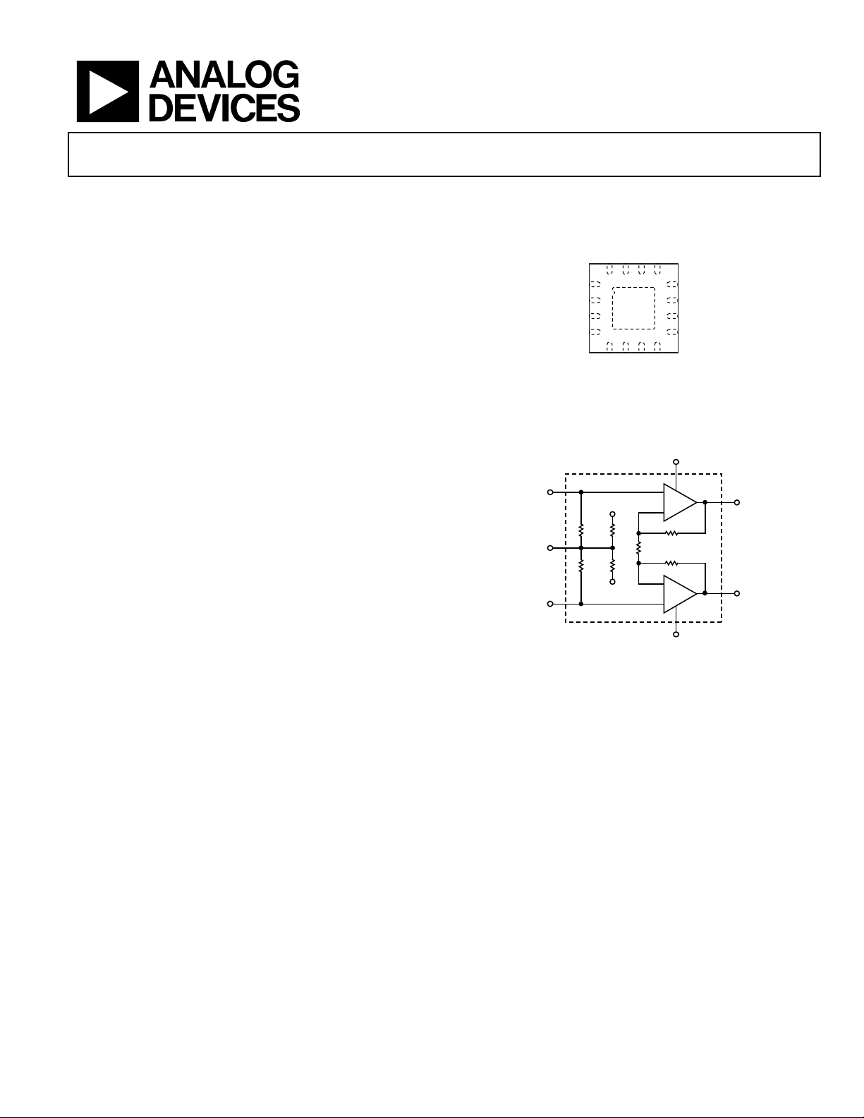
AD8396
PIN CONFIGURATION
VCOM-A
PD_A
VCC
51
41
TOP
VIEW
7
6
B
PD_B
VCOM-
Figure 1.
VOPA
31
8
VEE
CC
AV = 13
VEE
12
VONA
11
DGND
10
VOPB
9
VONB
07022-001
VOPA
VONA
07022-002
61
1
INPA
2
INNA
DGND
INPB
AD8396
3
4
5
INNB
INPA
VCOM-A
INNA
Figure 2. Channel A Internal Schematics
VCC
4k
4k
VEE
Rev. C
Information furnished by Analog Devices is believed to be accurate and reliable. However, no
responsibility is assumed by Analog Devices for its use, nor for any infringements of patents or other
rights of third parties that may result from its use. Specifications subject to change without notice. No
license is granted by implication or otherwise under any patent or patent rights of Analog Devices.
Trademarks and registered trademarks are the property of their respective owners.
One Technology Way, P.O. Box 9106, Norwood, MA 02062-9106, U.S.A.
Tel: 781.329.4700 www.analog.com
Fax: 781.461.3113 ©2007–2009 Analog Devices, Inc. All rights reserved.
Page 2

AD8396
TABLE OF CONTENTS
Features .............................................................................................. 1
Applications ....................................................................................... 1
General Description ......................................................................... 1
Pin Configuration ............................................................................. 1
Revision History ............................................................................... 2
Specifications ..................................................................................... 3
Absolute Maximum Ratings ............................................................ 4
Thermal Resistance ...................................................................... 4
Maximum Power Dissipation ..................................................... 4
ESD Caution .................................................................................. 4
Pin Configuration and Function Descriptions ............................. 5
REVISION HISTORY
8/09—Revision C: Initial Version
Typical Performance Characteristics ..............................................6
Theory of Operation .........................................................................8
Applications Information .................................................................9
Supplies, Grounding, and Layout ................................................9
Power Management ......................................................................9
Typical ADSL/ADSL2+ Application ...........................................9
Multitone Power Ratio (MTPR) ..................................................9
Lightning and AC Power Fault ................................................. 10
Outline Dimensions ....................................................................... 11
Ordering Guide .......................................................................... 11
Rev. C | Page 2 of 12
Page 3

AD8396
SPECIFICATIONS
(VCC − VEE) = 24 V, RL = 100 Ω, G
Table 1.
Parameter Min Typ Max Unit Test Conditions/Comments
DYNAMIC PERFORMANCE
−3 dB Small-Signal Bandwidth 8 MHz V
−3 dB Large-Signal Bandwidth 8 MHz V
Slew Rate 170 V/μs V
Differential Gain 12.8 13 13.2 V/V
NOISE/DISTORTION PERFORMANCE
Second Harmonic Distortion −90 dBc fC = 2 MHz, V
Third Harmonic Distortion −62 dBc fC = 2 MHz, V
Multitone Input Power Ratio (MTPR) −66 dBc
Differential Output Noise 140 nV/√Hz f = 10 kHz
INPUT CHARACTERISTICS
RTO Offset Voltage −15 −0.7 +15 mV Single-ended
−15 +0.3 +15 mV Differential
RTO Offset Voltage @ PD = (1) −30 +0.1 +30 mV Differential
Input Bias Current −5 −1.5 +5 μA
Input Resistance 8 kΩ Differential
Input Capacitance 1 pF Differential
OUTPUT CHARACTERISTICS
Differential Output Voltage Swing 42.6 43.4 44 V p-p ΔV
Single-Ended Output Voltage Swing 21.3 21.7 22 V p-p ΔV
Output Leakage Current −100 +100 μA PD = (1)
POWER SUPPLY
Operating Range, Dual Supply ±6 ±12 V
Operating Range, Single Supply 12 24 V
Total Quiescent Current
PD = (0) 9.0 10.8 13.0 mA
PD = (1) Shutdown State 0 1.4 3.0 mA
Common-Mode Voltage −10 +0.2 +10 mV VCM
PD = (0) Threshold 0.8 V (0) = 0 V
PD = (1) Threshold 1.6 V (1) = 5 V
PD = (0) Input Current −100 −47 +100 μA (0) = 0 V
PD = (1) Input Current −100 +1 +100 μA (1) = 5 V
+Power Supply Rejection Ratio −80 −60 dB ΔV
−Power Supply Rejection Ratio −80 −60 dB ΔV
= 13 (fixed), PD = (0), T = 25°C, typical DSL application circuit, unless otherwise noted.
DIFF
= 0.1 V p-p, differential
OUT
= 2 V p-p, differential
OUT
= 4 V p-p, differential
OUT
= 2 V p-p, differential
OUT
= 2 V p-p, differential
OUT
26 kHz to 2.2 MHz, Z
= 100 Ω, differential
LINE
load
, RL = 100 Ω
OUT
, RL = 50 Ω
OUT
/ΔVCC, ΔVCC = ±1 V, differential
OS, DM (RTI)
/ΔVEE, ΔVEE = ±1 V, differential
OS, DM (RTI)
Rev. C | Page 3 of 12
Page 4
AD8396
ABSOLUTE MAXIMUM RATINGS
Table 2.
Parameter Rating
Supply Voltage, VCC − VEE 26.4 V
Power Dissipation See Figure 3
Storage Temperature Range −65°C to +150°C
Operating Temperature Range −40°C to +85°C
Lead Temperature (Soldering, 10 sec) 300°C
Junction Temperature 150°C
Stresses above those listed under Absolute Maximum Ratings
may cause permanent damage to the device. This is a stress
rating only; functional operation of the device at these or any
other conditions above those indicated in the operational
section of this specification is not implied. Exposure to absolute
maximum rating conditions for extended periods may affect
device reliability.
THERMAL RESISTANCE
θJA is specified in still air with exposed pad soldered to 4-layer
JEDEC test board. θ
is specified at the exposed pad.
JC
Table 3.
Package Type θJA θ
Unit
JC
16-Lead LFCSP 56 9.1 °C/W
MAXIMUM POWER DISSIPATION
The maximum safe power dissipation for the AD8396 is limited
by its junction temperature on the die.
The maximum safe junction temperature of plastic encapsulated
devices, as determined by the glass transition temperature of the
plastic, is 150°C. Exceeding this limit can temporarily cause a shift
in the parametric performance due to a change in the stresses
exerted on the die by the package. Exceeding this limit for an
extended period can result in device failure.
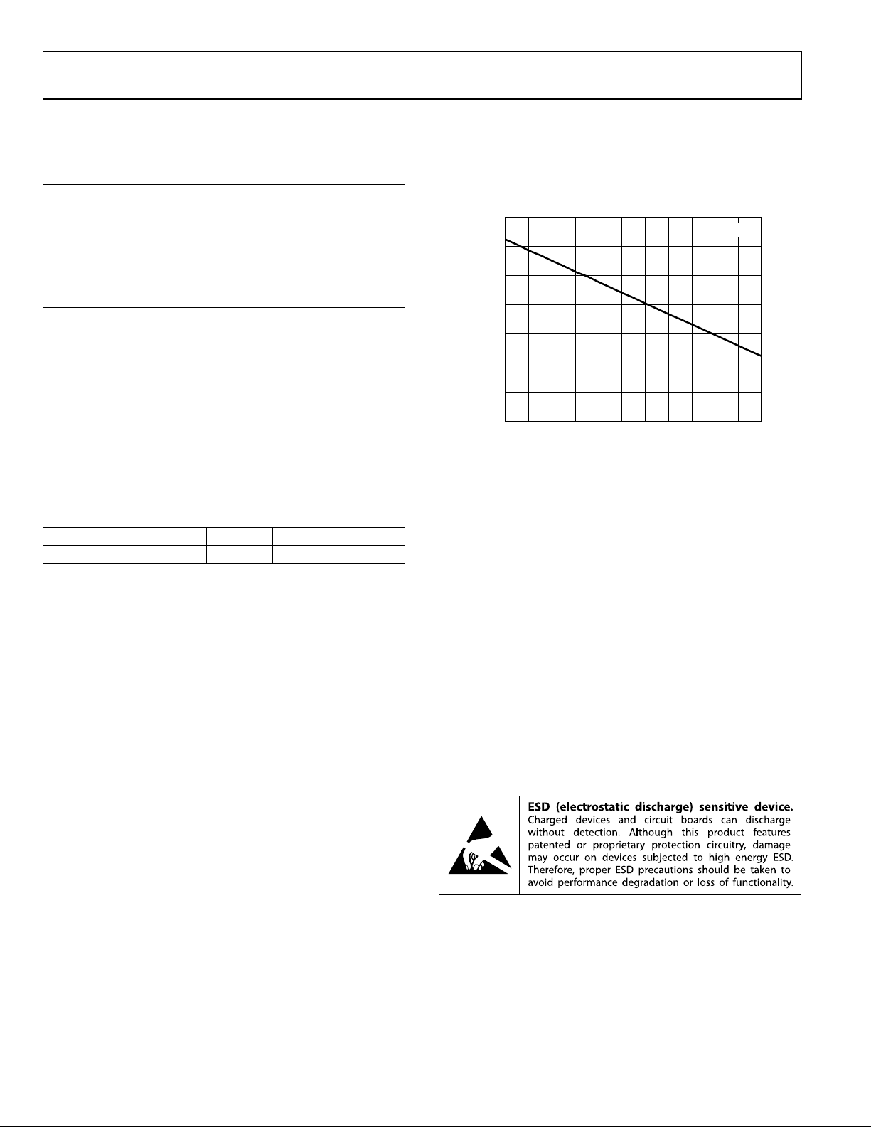
Figure 3 shows the maximum power dissipation in the package
vs. the ambient temperature for the 16-lead LFCSP on a JEDEC
standard 4-layer board. θ
3.5
3.0
2.5
2.0
1.5
1.0
MAXIMUM POW ER DISSIPAT ION (W)
0.5
0
–25 85
–15–5 5 15253545556575
Figure 3. Maximum Power Dissipation vs.
Ambient Temperature for a 4-Layer Board
values are approximations.
JA
AMBIENT TEMPERATURE (°C)
TJ = 150°C
07022-003
The power dissipated in the package (PD) is the sum of the
quiescent power dissipation and the power dissipated in the
package due to the load drive for all outputs. The quiescent
power is the voltage between the supply pins (V
quiescent current (I
to midsupply, the total drive power is V
). Assuming that the load RL is referenced
S
/2 × I
S
is dissipated in the package and part in the load (V
RMS output voltages should be considered. If R
V
, as in single-supply operation, the total power is VS × I
EE
In single supply with R
to VEE, worst case is V
L
Airflow increases heat dissipation, effectively reducing θ
) times the
S
, part of which
OUT
× I
OUT
OUT
is referenced to
L
= VS/2.
OUT
JA
OUT
. In
).
.
addition, more copper in direct contact with the package leads
from PCB traces, through-holes, ground, and power planes
reduces θ
.
JA
ESD CAUTION
Rev. C | Page 4 of 12
Page 5

AD8396
T
A
T
PIN CONFIGURATION AND FUNCTION DESCRIPTIONS
D_A
VCOM-A
P
VCC
61
VOPA
31
51
41
1
INPA
2
INNA
DGND
INPB
NOTE
HE EXPOSED PAD I S NOT CONNECT ED INTERNALLY.
FOR INCREASED RE LIABILITY OF THE SOLDE R JOINTS
ND MAXIMUM THERM AL CAPABILITY IT IS RECOMMENDED
HAT THE PAD BE SOLDERED TO T HE GROUND PLANE .
AD8396
5
INNB
TOP
VIEW
6
VCOM-B
7
PD_B
3
4
VONA
12
DGND
11
10
VOPB
9
VONB
8
VEE
4
07022-00
Figure 4. Pin Configuration
Table 4. Pin Function Descriptions
Pin No. Mnemonic Description
1 INPA Port A Input P
2 INNA Port A Input N
3, 11 DGND Ground
4 INPB Port B Input P
5 INNB Port B Input N
6 VCOM-B Port B Bias
7 PD_B Port B Shutdown
8 VEE Negative Power Supply
9 VONB Port B Output N
10 VOPB Port B Output P
12 VONA Port A Output N
13 VOPA Port A Output P
14 VCC Positive Power Supply
15 PD_A Port A Shutdown
16 VCOM-A Port A Bias
Exposed Pad No Connection
Rev. C | Page 5 of 12
Page 6
AD8396
–
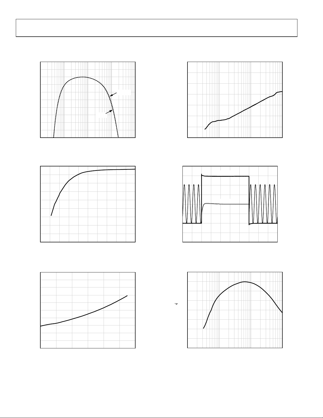
TYPICAL PERFORMANCE CHARACTERISTICS
2
1
0
–1
–2
–3
–4
–5
NORMALIZE D GAIN (dB)
–6
–7
–8
01
0.1 1 10
FREQUENCY (MHz)
2V p-p
0.1V p-p
07022-005
00
Figure 5. Differential Gain vs. Frequency, RL = 100 Ω
45
40
35
30
25
20
15
OUTPUT SWING (V p-p)
10
5
0
10 20 30 40 50 60 70 80 90
01
LOAD ()
07022-006
00
Figure 6. DC Differential Output Swing vs. Load
1000
900
800
700
600
500
400
300
200
INTERNAL PO WER CONSUMPT ION (mW)
100
0
10 22
12 14 16 18 20
OUTPUT PO WER (dBm)
07022-007
Figure 7. Internal Power Consumption vs. Output Power,
Typical ADSL/ADSL2+ Application Circuit, 100 Ω Resistive Load Only
30
–40
–50
–60
–70
CROSSTALK (d B)
–80
–90
–100
0.01 10
0.1 1
FREQUENCY (MHz)
07022-008
Figure 8. Crosstalk vs. Frequency, Typical ADSL/ADSL2+ Application Circuit,
= 2 V p-p, RL = 100 Ω
V
OUT
6
5
4
3
(V)
2
PD
V
1
0
–1
–2
02
24681012141618
PD PULSE
OUTPUT
TIME (s)
2.0
1.5
1.0
0.5
(V)
0
OUT
V
–0.5
–1.0
–1.5
–2.0
0
07022-009
Figure 9. Power-Down/Power-Up Transition
160
140
120
100
80
60
NOISE (nV/ Hz)
40
20
0
0.01 10
0.1 1
FREQUENCY (MHz)
07022-010
Figure 10. Differential Output Noise vs. Frequency,
Typical ADSL/ADSL2+ Application Circuit
Rev. C | Page 6 of 12
Page 7
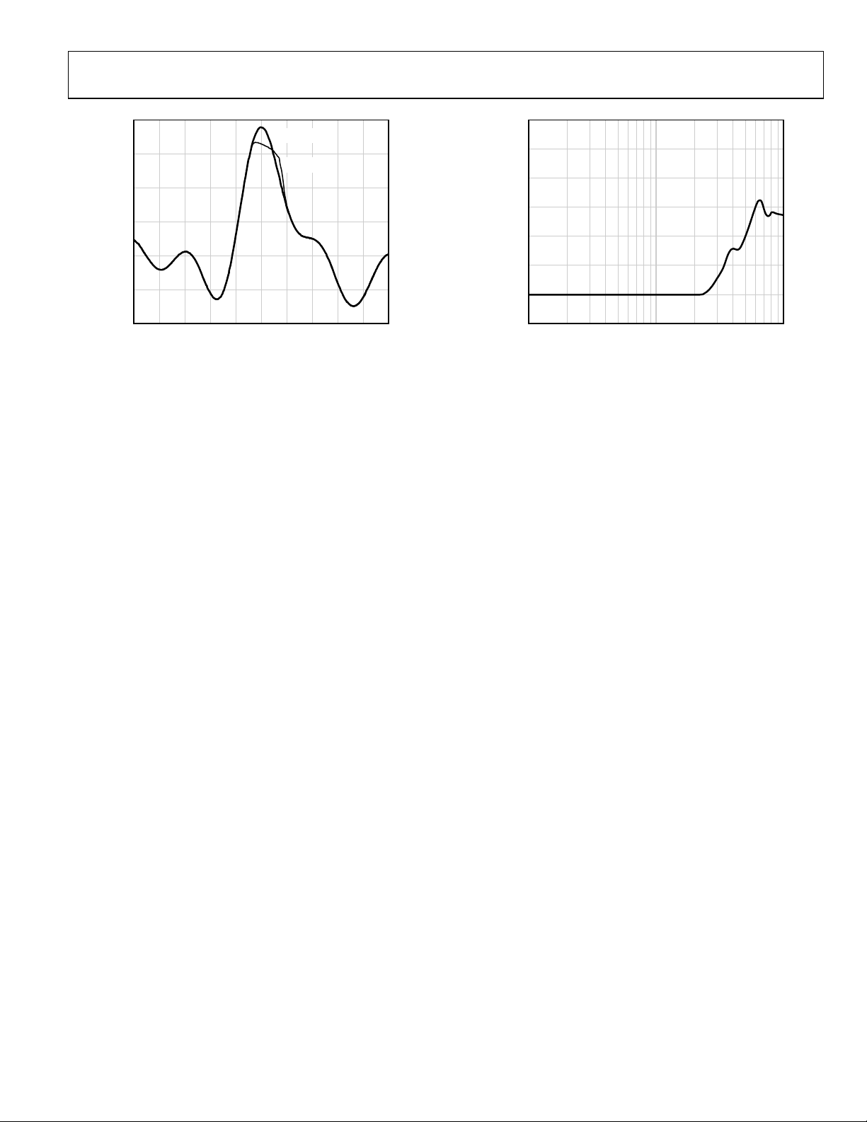
AD8396
–
20
15
10
5
AMPLITUDE ( V)
0
–5
–10
02.0
0.2 0.4 0.6 0.8 1.0 1.2 1.4 1.6 1.8
VS = ±12V
VS = ±10V
TIME (s)
Figure 11. Output Overdrive Recovery, Typical ADSL/ADSL2+
Application Circuit, V
OUT
= 3.3 V
, CF = 5.47, RL = 100 Ω
RMS
40
–50
–60
–70
–80
FEEDTHROUG H (dB)
–90
–100
07022-011
–110
0.1 10
1
FREQUENCY (MHz)
07022-012
Figure 12. Feedthrough vs. Frequency,
Typical ADSL/ADSL2+ Application Circuit,
= 2 V p-p, RL = 100 Ω
V
OUT
Rev. C | Page 7 of 12
Page 8
AD8396
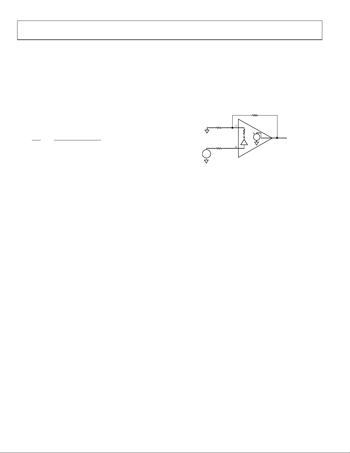
THEORY OF OPERATION
The AD8396 is a current feedback amplifier with high output
current capability. With a current feedback amplifier, the
current into the inverting input is the feedback signal, and the
open-loop behavior is that of a transimpedance, dV
/dIIN or TZ.
O
The open-loop transimpedance is analogous to the open-loop
voltage gain of a voltage feedback amplifier. Figure 13 shows a
simplified model of a current feedback amplifier. Because R
proportional to 1/g
where g
is the transconductance of the input stage. Basic
m
, the equivalent voltage gain is TZ × gm,
m
IN
analysis of the follower with the gain circuit yields
(S)
V
O
G
V
×=
IN
T
Z
Z
IN
)((S)
RRGT
+×+
F
where:
G = 1 + R
R
IN
F/RG
= 1/gm ≈ 50 Ω
is
Because G × R
has relatively constant bandwidth vs. gain. The 3 dB point is set
when |T
Z
In a nonideal amplifier, there are additional poles that contribute
excess phase, and there is a value for R
is unstable. Tolerance for peaking and desired flatness determines
the optimum R
<< RF for low gains, a current feedback amplifier
IN
| = RF.
below which the amplifier
F
in each application.
F
R
F
R
G
R
IN
T
Z
I
R
N
V
IN
Figure 13. Simplified Block Diagram
IN
V
OUT
7022-013
Rev. C | Page 8 of 12
Page 9
AD8396
APPLICATIONS INFORMATION
SUPPLIES, GROUNDING, AND LAYOUT
The AD8396 can be powered from either single or dual supplies,
with the total supply voltage ranging from 12 V to 24 V. For
optimum performance, use well-regulated low ripple supplies.
As with all high speed amplifiers, pay close attention to supply
decoupling, grounding, and overall board layout. Provide low
frequency supply decoupling with 10 μF tantalum capacitors
from each supply to ground. In addition, decouple all supply
pins with 0.1 μF quality ceramic chip capacitors placed as close
as possible to the driver. Use an internal low impedance ground
plane to provide a common ground point for all driver and
decoupling capacitor ground requirements. Whenever possible,
use separate ground planes for analog and digital circuitry.
Follow high speed layout techniques to minimize parasitic
capacitance.
Keep input and output traces as short as possible and as far
apart from each other as practical to minimize crosstalk. Keep
all differential signal traces as symmetrical as possible.
POWER MANAGEMENT
A digitally programmable logic pin switches each port of the
AD8396 between active bias and shutdown states. The PD_A
pin controls Port A and the PD_B pin controls Port B. These
pins can be controlled directly with either 3.3 V or 5 V CMOS
logic with the DGND pins as a reference. If left unconnected,
the PD pins float high, placing the amplifier in the shutdown
state. See the Specifications section for the quiescent current for
each of the available bias states.
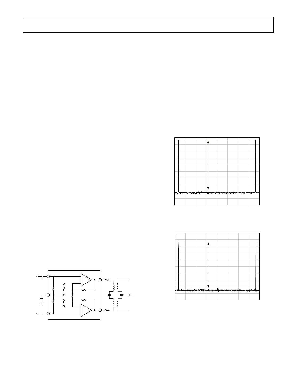
TYPICAL ADSL/ADSL2+ APPLICATION
In a typical ADSL/ADSL2+ application, a differential line driver
takes the signal from the analog front end (AFE) and drives it
onto the twisted pair telephone line. Referring to the typical
circuit representation in Figure 14, the differential input appears
and V
at V
IN+
transformer coupled to the telephone line at TIP and RING.
The common-mode operating point, generally midway between
the supplies, is set internally and is available at VCOM.
V
IN+
VCOM
0.1µF
V
IN–
from the AFE, while the differential output is
IN−
4k
4k
VCC
VEE
+
–
–
+
R
m
1:N
R
m
Figure 14. Typical ADSL/ADSL2+ Application Circuit
TIP
RING
R
OUT
07022-014
MULTITONE POWER RATIO (MTPR)
The DMT signal used in ADSL/ADSL2+ systems carries data in
discrete tones or bins, which appear in the frequency domain in
evenly spaced 4.3125 kHz intervals. In applications using this type
of waveform, MTPR is a commonly used measure of linearity.
Generally, designers are concerned with two types of MTPR:
in-band and out-of-band. In-band MTPR is defined as the
measured difference from the peak of one tone that is loaded
with data to the peak of an adjacent tone that is intentionally
left empty. Out-of-band MTPR is more loosely defined as the
spurious emissions that occur in the receive band located between
25.875 kHz and the first downstream tone at 138 kHz. Figure 15
and Figure 16 show the AD8396 in-band MTPR for a 5.5 crest
factor waveform for empty bins in the ADSL and extended
ADSL2+ bandwidths.
0
–10
–20
–30
–40
–50
–60
MAGNITUDE (d Bm)
–70
–80
–90
–100
642.131 651.619
644.503 646.875 649.247
Figure 15. In-Band MTPR at 646.875 kHz
0
–10
–20
–30
–40
–50
–60
MAGNITUDE (d Bm)
–70
–80
–90
–100
1.9618 1.9712
1.9641 1.9665 1.9689
Figure 16. In-Band MTPR at 1.9665 MHz
–73dBc
FREQUENCY (kHz)
–68dBc
FREQUENCY (MHz )
07022-015
07022-016
Rev. C | Page 9 of 12
Page 10

AD8396
LIGHTNING AND AC POWER FAULT
When the AD8396 is an ADSL/ADSL2+ line driver, it is
transformer coupled to the twisted pair telephone line. In this
environment, the AD8396 is subject to large line transients,
resulting from events, such as lightning strikes or downed
power lines. Additional circuitry is required to protect the
AD8396 from damage due to these events.
Rev. C | Page 10 of 12
Page 11

AD8396
OUTLINE DIMENSIONS
PIN 1
INDICATOR
0.80
0.75
0.70
SEATING
PLANE
4.10
4.00 SQ
3.90
0.65
BSC
0.50
0.40
0.30
0.05 MAX
0.02 NOM
0.20 REF
0.35
0.30
0.25
13
12
9
8
BOTTOM VIEWTOP VIEW
COPLANARITY
0.08
N
1
P
I
D
C
I
A
N
I
16
1
EXPOSED
PAD
FOR PROPER CONNECTION OF
THE EXPOSED PAD, REFER TO
THE PIN CONFIGURATION AND
FUNCTION DESCRIPTIONS
SECTION OF THIS DATA SHEET.
2.60
2.50 SQ
2.40
4
5
R
O
T
COMPLIANTTOJEDEC STANDARDS MO-220-WGGC.
042709-A
Figure 17. 16-Lead Lead Frame Chip Scale Package [LFCSP_WQ]
4 mm × 4 mm, Very Very Thin Quad
(CP-16-26)
Dimensions shown in millimeters
ORDERING GUIDE
Model Temperature Range Package Description Package Option
AD8396ACPZ-R2
AD8396ACPZ-RL
AD8396ACPZ-R7
1
Z = RoHS Compliant Part.
1
−40°C to +85°C 16-Lead Lead Frame Chip Scale Package (LFCSP_WQ) CP-16-26
1
−40°C to +85°C 16-Lead Lead Frame Chip Scale Package (LFCSP_WQ) CP-16-26
1
−40°C to +85°C 16-Lead Lead Frame Chip Scale Package (LFCSP_WQ) CP-16-26
Rev. C | Page 11 of 12
Page 12

AD8396
NOTES
©2007–2009 Analog Devices, Inc. All rights reserved. Trademarks and
registered trademarks are the property of their respective owners.
D07022-0-8/09(C)
Rev. C | Page 12 of 12
 Loading...