

Page 1
a
Fast, High Voltage Drive, 6-Channel Output
TM
DecDriver
Decimating LCD Panel Driver
AD8381
FEATURES
High Voltage Drive:
Rated Settling Time to within 1.3 V of Supply Rails
Output Overload Protection
High Update Rates:
Fast, 100 Ms/s 10-Bit Input Word Rate
Low Power Dissipation: 570 mW
Includes STBY Function
Voltage Controlled Video Reference (Brightness) and
Full-Scale (Contrast) Output Levels
3.3 V or 5 V Logic and 9 V–18 V Analog Supplies
High Accuracy:
Laser Trimming Eliminates External Calibration
Flexible Logic:
INV Reverses Polarity of Video Signal
STSQ/XFR for Parallel AD8381 Operation in
12-Channel Systems
Drives Capacitive Loads:
27 ns Settling Time to 1% into 150 pF Load
Slew Rate 265 V/s with 150 pF Load
Available in 48-Lead LQFP
APPLICATIONS
LCD Analog Column Driver
PRODUCT DESCRIPTION
The AD8381 provides a fast, 10-bit latched decimating digital
input, which drives six high voltage outputs. Ten-bit input
words are sequentially loaded into six separate high-speed, bipolar
DACs. Flexible digital input format allows several AD8381s to be
used in parallel for higher resolution displays. STSQ synchronizes
sequential input loading, XFR controls synchronous output
updating and R/L controls the direction of loading as either
Left to Right or Right to Left. Six channels of high voltage
output drivers drive to within 1.3 V of the rail in rated settling
time. The output signal can be adjusted for brightness, signal
inversion and contrast for maximum flexibility.
The AD8381 is fabricated on ADI’s proprietary, fast bipolar
24 V process, providing fast input logic, bipolar DACs with
trimmed accuracy and fast settling, high voltage precision drive
amplifiers on the same chip.
The AD8381 dissipates 570 mW nominal static power. STBY
pin reduces power to a minimum, with fast recovery.
The AD8381 is offered in a 48-lead 7 × 7 × 1.4 mm LQFP
package and operates over the commercial temperature range of
0°C to 85°C.
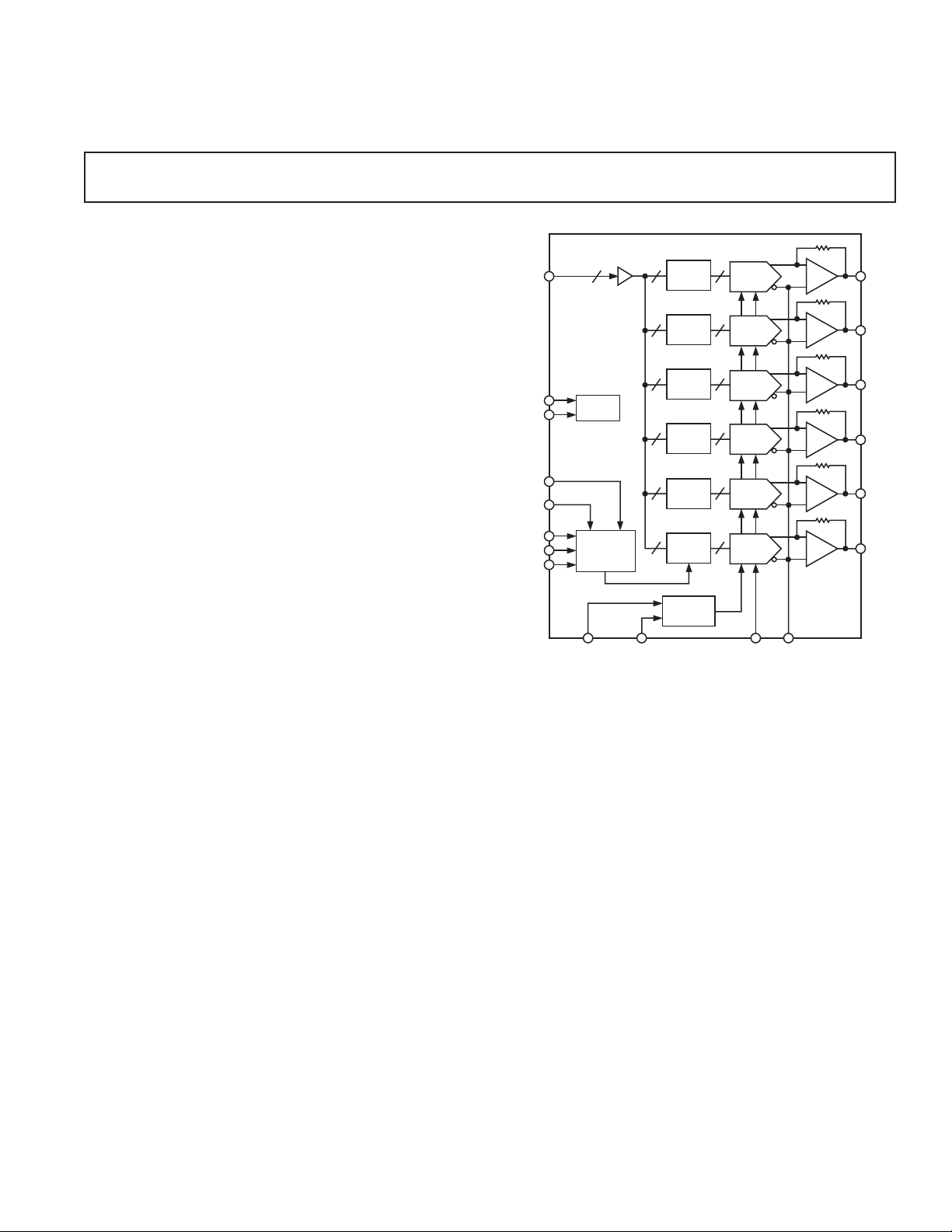
DB (0:9)
STBY
BYP
E/O
L/R
CLK
STSQ
XFR
FUNCTIONAL BLOCK DIAGRAM
10
AD8381
BIAS
SEQUENCE
CONTROL
VREFHI VREFLO INV VMID
10
10
10
10
10
10
CONTROL
2-STAGE
LATCH
2-STAGE
LATCH
2-STAGE
LATCH
2-STAGE
LATCH
2-STAGE
LATCH
2-STAGE
LATCH
SCALING
10
DAC
10
DAC
10
DAC
10
DAC
10
DAC
10
DAC
VID0
VID1
VID2
VID3
VID4
VID5
DecDriver is a trademark of Analog Devices, Inc.
REV. 0
Information furnished by Analog Devices is believed to be accurate and
reliable. However, no responsibility is assumed by Analog Devices for its
use, nor for any infringements of patents or other rights of third parties that
may result from its use. No license is granted by implication or otherwise
under any patent or patent rights of Analog Devices.
One Technology Way, P.O. Box 9106, Norwood, MA 02062-9106, U.S.A.
Tel: 781/329-4700www.analog.com
Fax: 781/326-8703 © Analog Devices, Inc., 2002
Page 2
(@ 25ⴗC, AVCC = 15.5 V, DVCC = 3.3 V, VREFLO = VMID = 7 V, VREFHI = 9.5 V,
T
AD8381–SPECIFICATIONS
= 0ⴗC, T
MIN
Model Conditions Min Typ Max Unit
VIDEO DC PERFORMANCE
1
T
to T
MIN
MAX
VDE DAC Code 450 to 800 –7.5 +1.0 +7.5 mV
VCME DAC Code 450 to 800 –3.5 +0.5 +3.5 mV
REFERENCE INPUTS (VREFHI–VREFLO) = 2.5 V
VMID Range
2
VMID Bias Current 35 77 µA
VREFHI VREFLO AVCC V
VREFLO VMID – 0.5 VREFHI V
VREFHI Input Resistance to VREFLO 20 kΩ
VREFLO Bias Current 0.01 0.07 µA
VREFHI Input Current 125 165 µA
VFS Range
3
RESOLUTION
Coding Binary 10 Bits
DIGITAL INPUT CHARACTERISTICS CLK Rise and Fall Time = 5 ns
Input Data Update Rate NRZ 100 Ms/s
CLK to Data Setup Time: t
CLK to STSQ Setup Time: t
CLK to XFR Setup Time: t
CLK to Data Hold Time: t
CLK to STSQ Hold Time: t
CLK to XFR Hold Time: t
C
IN
I
IH
I
IL
V
IH
V
IL
V
TH
1
3
5
2
4
6
Threshold Voltage 1.4 V
VIDEO OUTPUT CHARACTERISTICS
Output Voltage Swing AVCC – VOH, VOL – AGND 1 1.3 V
CLK to VID Delay4: t
7
50% of VIDx 13.5 15.5 17.5 ns
INV to VID Delay 50% of VIDx 12 14 16 ns
Output Current 30 75 mA
Output Resistance 29 Ω
VIDEO OUTPUT DYNAMIC PERFORMANCE T
MIN
to T
, VO = 5 V Step, CL = 150 pF
MAX
Data Switching Slew Rate 265 V/µs
Invert Switching Slew Rate 410 V/µs
Data Switching Settling Time to 1% 27 32 ns
Data Switching Settling Time to 0.25% 50 75 ns
Invert Switching Settling Time to 1% 33 40 ns
Invert Switching Settling Time to 0.25% 55 100 ns
CLK and Data Feedthrough
All-Hostile Crosstalk
5
6
Amplitude 50 mV p-p
Glitch Duration 45 ns
POWER SUPPLY
Supply Rejection (VDE) AVCCx = +15.5 V ± 1 V 0.6 mV/V
DVCC, Operating Range 3 5.5 V
DVCC, Quiescent Current 18 25 mA
AVCC, Operating Range 918V
Total AVCC Quiescent Current 33 40 mA
STBY AVCC Current STBY = H 1.8 3 mA
STBY DVCC Current STBY = H 0.03 0.1 mA
OPERATING TEMPERATURE RANGE 0 85 °C
NOTES
1
VDE = Differential Error Voltage. VCME = Common-Mode Error Voltage. See the Functional Description section.
2
See Figure 6 in the Functional Description section.
3
VFS = 2 × (VREFHI–VREFLO). See Functional Description section.
4
Measured from 50% of falling CLK edge to 50% of output change. Measurement is made for both states of INV.
5
Measured on one output as CLK is driven and STSQ and XFR are held LOW.
6
Measured on one output as the other five are changing from 000
Specifications subject to change without notice.
HEX
to 3FF
= 85ⴗC, unless otherwise noted.)
MAX
for both states of INV.
HEX
6.25 9.25 V
0 5.75 V
0ns
0ns
0ns
5ns
5ns
5ns
3pF
0.6 0.7 µA
0.05 0.16 µA
2.0 V
0.08 V
5 mV p-p
–2–
REV. 0
Page 3
AD8381
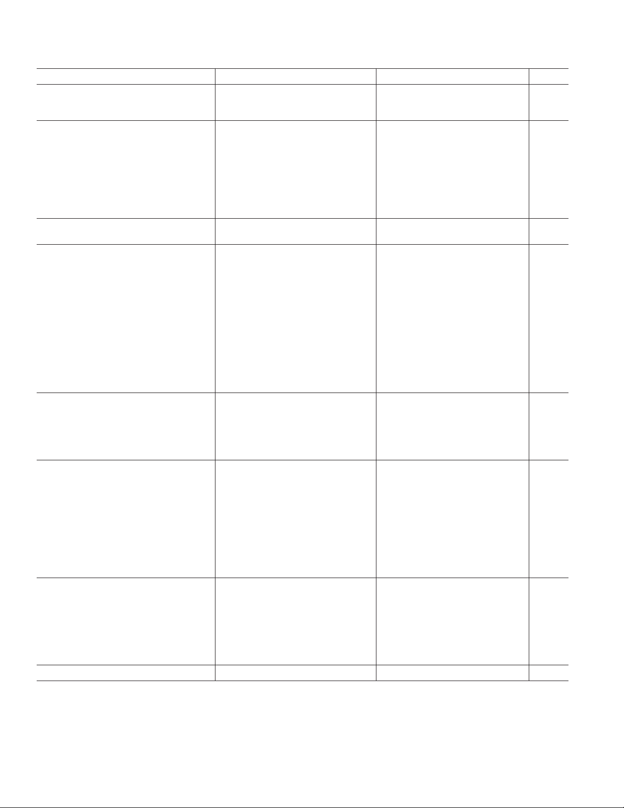
TIMING CHARACTERISTICS
Parameter Conditions Min Typ Max Unit
CLK to Data Setup Time CLK Rise and Fall Time = 5 ns 0 ns
t
1
t2CLK to Data Hold Time CLK Rise and Fall Time = 5 ns 5 ns
CLK to STSQ Setup Time CLK Rise and Fall Time = 5 ns 0 ns
t
3
CLK to STSQ Hold Time CLK Rise and Fall Time = 5 ns 5 ns
t
4
t5CLK to XFR Setup Time CLK Rise and Fall Time = 5 ns 0 ns
CLK to XFR Hold Time CLK Rise and Fall Time = 5 ns 5 ns
t
6
t7CLK to VID Delay 13.5 15.5 17.5 ns
DB (0:9)
CLK
STSQ, XFR
DB (0:9)
CLK
STSQ
XFR
–1 0
t3,t
t
1
t
2
t4,t
5
6
Figure 1. Timing Requirement E/O = HIGH
–1
t
1
t
3
t
5
t
6
t
2
t
4
0
Figure 2. Timing Requirements E/O = LOW
REV. 0
CLK
XFR
VIDx
t
7
Figure 3. Output Timing
–3–
Page 4
AD8381
ABSOLUTE MAXIMUM RATINGS
1
Supply Voltages
AVCCx – AGND . . . . . . . . . . . . . . . . . . . . . . . . . . . . . 19 V
DVCC – DGND . . . . . . . . . . . . . . . . . . . . . . . . . . . . . . 5.5 V
Input Voltages
Maximum Digital Input Voltages . . . . . . . . DVCC + 0.5 V
Minimum Digital Input Voltages . . . . . . . . DGND – 0.5 V
Maximum Analog Input Voltages . . . . . . . . . AVCC + 0.5 V
Minimum Analog Input Voltages . . . . . . . . AGND – 0.5 V
Internal Power Dissipation
2
LQFP Package @ 25°C Ambient . . . . . . . . . . . . . . . . 2.7 W
Output Short Circuit Duration . . . . . . . . . . . . . . . . . . Infinite
Operating Temperature Range . . . . . . . . . . . . . . 0°C to 85°C
Storage Temperature Range . . . . . . . . . . . . –65°C to +125°C
Lead Temperature Range (Soldering 10 sec) . . . . . . . . 300°C
NOTES
1
Stresses above those listed under the Absolute Maximum Ratings may cause
permanent damage to the device. This is a stress rating only; functional operation
of the device at these or any other conditions above those indicated in the
operational section of this specification is not implied. Exposure to the absolute
maximum ratings for extended periods may reduce device reliability.
2
48-lead LQFP Package:
θJA = 45°C/W (Still Air, 4-Layer PCB)
θJC = 19°C/W
Overload Protection
The AD8381 employs a two-stage overload protection circuit
that consists of an output current limiter and a thermal shutdown.
The maximum current at any one output of the AD8381 is
internally limited to 100 mA average. In the event of a momentary short-circuit between a video output and a power supply rail
(VCC or AGND), the output current limit is sufficiently low to
provide temporary protection.
The thermal shutdown “debiases” the output amplifier when the
junction temperature reaches the internally set trip point. In the
event of an extended short-circuit between a video output and a
power supply rail, the output amplifier current continues to
switch between 0 mA and 100 mA typ with a period determined by
the thermal time constant and the hysteresis of the thermal trip
point. The thermal shutdown provides long term protection by
limiting the average junction temperature to a safe level.
Recovery from a momentary short-circuit is fast, approximately
100 ns. Recovery from a thermal shutdown is slow and is
dependent on the ambient temperature.
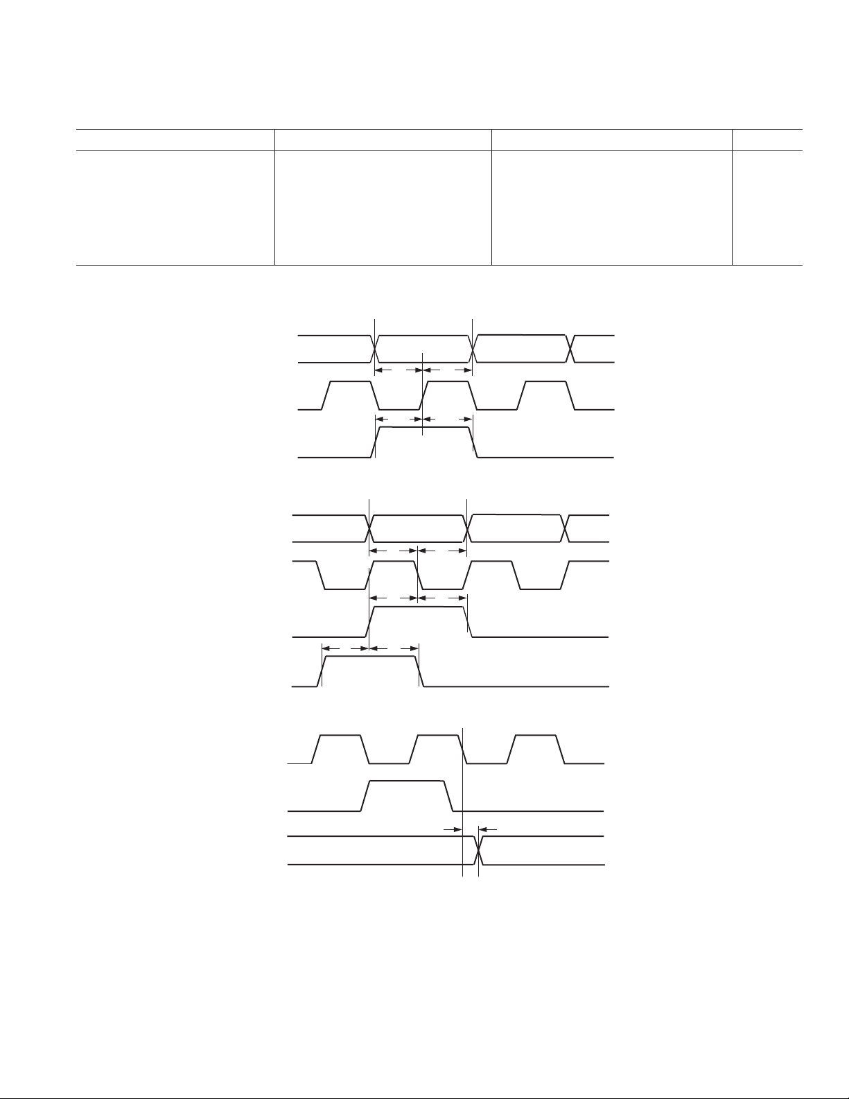
MAXIMUM POWER DISSIPATION
The maximum power that can be safely dissipated by the AD8381
is limited by its junction temperature. The maximum safe junction temperature for plastic encapsulated devices is determined
by the glass transition temperature of the plastic, approximately
150°C. Exceeding this limit temporarily may cause a shift in the
parametric performance due to a change in the stresses exerted
on the die by the package. Exceeding a junction temperature of
175°C for an extended period can result in device failure.
To ensure proper operation within the specified operating temperature range, it is necessary to limit the maximum power
dissipation as follows:
P
DMAX
= (T
JMAX
– TA)/θ
JA
where
T
= 150°C.
JMAX
3.5
3.0
2.5
2.0
1.5
1.0
MAXIMUM POWER DISSIPATION – W
0.5
0
10 20 30 40 50 60 70 80 90
AMBIENT TEMPERATURE – ⴗC
Figure 4. Maximum Power Dissipation vs. Temperature
ORDERING GUIDE
Temperature Package Package
Model Range Description Option
AD8381AST 0°C to 85°C 48-Lead LQFP ST-48
AD8381AST-REEL
Reel
CAUTION
ESD (electrostatic discharge) sensitive device. Electrostatic charges as high as 4000 V readily
accumulate on the human body and test equipment and can discharge without detection. Although
the AD8381 features proprietary ESD protection circuitry, permanent damage may occur on
devices subjected to high-energy electrostatic discharges. Therefore, proper ESD precautions are
recommended to avoid performance degradation or loss of functionality.
–4–
WARNING!
ESD SENSITIVE DEVICE
REV. 0
Page 5
AD8381
PIN FUNCTION DESCRIPTIONS
Pin No. Mnemonic Function Description
1, 12, 19, 23, NC No Connect
24, 43–45
2–11 DB (0:9) Data Input 10-Bit Data Input MSB = DB (9).
13 E/O Even/Odd Select The active CLK edge is the rising edge when this input is held HIGH
and it is the falling edge when this input is held LOW.
Data is loaded sequentially on the rising edges of CLK when this input
is HIGH and loaded on the falling edges when this input is LOW.
14 R/L Right/Left Select A new data loading sequence begins on the left, with Channel 0, when this
input is LOW, and on the right, with Channel 5 when this input is HIGH.
15 INV Invert When this pin is HIGH, the analog output voltages are above VMID.
When LOW, the analog output voltages are below VMID.
16 DGND Digital Supply Return This pin is normally connected to the analog ground plane.
17 DVCC Digital Power Supply Digital Power Supply.
18, 27, 31, AVCCx Analog Power Supplies Analog Power Supplies.
35, 42
20 STBY Standby When HIGH, the internal circuits are “debiased” and the power
dissipation drops to a minimum.
21 BYP Bypass A 0.1 µF capacitor connected between this pin and AGND ensures
optimum settling time.
22, 25, 29, AGNDx Analog Supply Returns These pins are normally connected to the analog ground plane.
33, 37, 41
26, 28, 30, VID5, VID4, VID3, Analog Outputs These pins are directly connected to the analog inputs of the LCD panel.
32, 34, 36 VID2, VID1, VID0
38 VMID Midpoint Reference The voltage applied between this pin and AGND sets the midpoint
reference of the analog outputs. This pin is normally connected to VCOM.
39 VREFLO Full-Scale Reference The voltage applied between Pins 39 and 40 sets the full-scale output voltage.
40 VREFHI Full-Scale Reference The voltage applied between Pins 39 and 40 sets the full-scale output voltage.
46 STSQ Start Sequence A new data loading sequence begins on the rising edge of CLK when
this input was HIGH on the preceding rising edge of CLK and the E/O
input is held HIGH.
A new data loading sequence begins on the falling edge of CLK when
this input was HIGH on the preceding falling edge of CLK and the E/O
input is held LOW.
47 XFR Data Transfer Data is transferred to the outputs on the immediately following falling
edge of CLK when this input is HIGH on the rising edge of CLK.
48 CLK Clock Clock Input.
REV. 0
48
1
NC
2
DB0
3
DB1
4
DB2
5
DB3
6
DB4
7
DB5
8
DB6
9
DB7
10
DB8
11
DB9
12
NC
13 14
NC = NO CONNECT
PIN CONFIGURATION
VMID
VREFLO
VREFHI
AGNDDAC
AV CC DAC
NC
NC
NC
STSQ
XFR
CLK
47 46
45 44 39 38 3743 42 41 40
PIN 1
IDENTIFIER
AD8381
TOP VIEW
(Not to Scale)
E/O
R/L
15 16 17 18
INV
DVC C
DGND
19 20
NC
AV CCBIAS
21 22
STBY
BYP
AGNDBIAS
23 24
NC
–5–
AGND0
NC
36
VID0
35
AV CC0, 1
34
VID1
33
AGND1, 2
32
VID2
31
AV CC2, 3
30
VID3
29
AGND3, 4
28
VID4
27
AV CC4, 5
26
VID5
25
AGND5
Page 6

AD8381
–Typical Performance Characteristics
12V
VMID = 7V
VFS = 5V
VIDx
2V
C
L
150pF
20ns/DIV
TPC 1. Invert Switching 10 V Step Response (Rise) at C
7V
VMID = 7V
VFS = 5V
VIDx
2V
C
L
150pF
12V
VMID = 7V
VFS = 5V
VIDx
2V
L
TPC 4. Invert Switching 10 V Step Response (Fall) at C
7V
VMID = 7V
VFS = 5V
VIDx
2V
C
L
150pF
20ns/DIV
C
L
150pF
L
10ns/DIV
TPC 2. Data Switching 5 V Step Response (Rise) at CL,
INV = L
12V
VMID = 7V
VFS = 5V
VIDx
7V
C
L
150pF
20ns/DIV
TPC 3. Data Switching 5 V Step Response (Rise) at CL,
INV = H
10ns/DIV
TPC 5. Data Switching 5 V Step Response (Fall) at CL,
INV = L
12V
VMID = 7V
VFS = 5V
VIDx
7V
C
L
150pF
20ns/DIV
TPC 6. Data Switching 5 V Step Response (Fall) at CL,
INV = H
–6–
REV. 0
Page 7

AD8381
20ns/DIV
+10mV
VMID = 7V
–10mV
DB (0:9)
0.25%
7V
0.00%
–0.25%
–0.50%
–0.75%
–1.00%
t = 0
VMID = 7V
VFS = 5V
VIDx
C
L
150pF
10ns/DIV
TPC 7. Output Settling Time (Rising Edge) at CL,
5 V STEP, INV = LOW
0.00%
12V
–0.25%
–0.50%
–0.75%
–1.00%
t = 0
VMID = 7V
VFS = 5V
VIDx
C
L
150pF
10ns/DIV
1.00%
0.75%
0.50%
0.25%
2V
0.00%
–0.25%
–0.50%
–0.75%
–1.00%
t = 0
VMID = 7V
VFS = 5V
VIDx
C
L
150pF
10ns/DIV
TPC 10. Output Settling Time (Falling Edge) at CL,
5 V STEP, INV = LOW
VMID = 7V
1.00%
0.75%
0.50%
0.25%
0.00%
–0.25%
–0.50%
–0.75%
7V
t = 0
VFS = 5V
VIDx
C
L
150pF
10ns/DIV
TPC 8. Output Settling Time (Rising Edge) at CL, 5 V Step,
INV = HIGH
+30mV
+20mV
+10mV
VMID = 7V
–10mV
–20mV
TPC 9. All-Hostile Crosstalk at C
VID5
VID0 – VID4
5V
20ns/DIV
L
TPC 11. Output Settling Time (Falling Edge) at CL,
5 V Step, INV = HIGH
TPC 12. Data Switching Transient (Feedthrough) at C
L
REV. 0
–7–
Page 8

AD8381
0.5
0.4
0.3
0.2
0.1
0.0
DNL – LSB
–0.1
–0.2
–0.3
–0.4
–0.5
0
256 512 768 1023
INPUT CODE
TPC 13. Differential Nonlinearity (DNL) vs. Code, INV = H
0.5
0.4
0.3
0.2
0.1
0.0
INL – LSB
–0.1
–0.2
–0.3
–0.4
–0.5
0
256 512 768 1023
INPUT CODE
TPC 14. Integral Nonlinearity (INL) vs. Code, INV = H
0.5
0.4
0.3
0.2
0.1
0.0
DNL – LSB
–0.1
–0.2
–0.3
–0.4
–0.5
0
256 512 768 1023
INPUT CODE
TPC 16. Differential Nonlinearity (DNL) vs. Code, INV = L
0.5
0.4
0.3
0.2
0.1
0.0
INL – LSB
–0.1
–0.2
–0.3
–0.4
–0.5
0
256 512 768 1023
INPUT CODE
TPC 17. Integral Nonlinearity (INL) vs. Code, INV = L
5
0
–5
–10
VFS = 4V
–15
–20
NORMALIZED VDE AT CODE 0 – mV
–25
5
VFS = 5V
VFS = 5.75V
67 1110
VMID – V
VFS = 5.75V
89
VFS = 4V
VFS = 5V
TPC 15. Normalized VDE at Code 0 vs. VMID, AVCC = 15.5 V
0
–20
–40
PSRR – dB
–60
–80
10k
CODE 512, INV = LOW
CODE 512, INV = HIGH
100k 1M 5M
FREQUENCY – Hz
TPC 18. AVCC Power Supply Rejection vs. Frequency
–8–
REV. 0
Page 9

7.5
INPUT CODE
3.50
0
VCME – mV
1.75
0.00
–1.75
512 768 1023256
–3.50
TEMPERATURE – ⴗC
3.50
0
VCME – mV
1.75
0.00
–1.75
40 60 10020
–3.50
80
CODE 512
5.0
2.5
0.0
VDE – mV
–2.5
–5.0
–7.5
0
512 768 1023256
INPUT CODE
TPC 19. Differential Error Voltage (VDE) vs. Code
7.5
5.0
AD8381
TPC 21. Common-Mode Error Voltage (VCME) vs. Code
2.5
CODE 512
0.0
VDE – mV
–2.5
–5.0
–7.5
0
40 60 10020
TEMPERATURE – ⴗC
80
TPC 20. Differential Error Voltage (VDE) vs. Temperature
TPC 22. Common-Mode Error (VCME) vs. Temperature
REV. 0
–9–
Page 10

AD8381
FUNCTIONAL DESCRIPTION
The AD8381 is a system building block designed to directly
drive the columns of LCD panels of the type popularized for use
in data projectors. It comprises six channels of precision 10-bit
digital-to-analog converters loaded from a single, high-speed,
10-bit-wide input. Precision current feedback amplifiers, providing well-damped pulse response and rapid voltage settling into
large capacitive loads, buffer the six outputs. Laser trimming at
the wafer level ensure low absolute output errors and tight channelto-channel matching. In addition, tight part-to-part matching
in high channel count systems is guaranteed by the use of an
external voltage reference.
INPUT DATA LOADING (STart SeQuence Control)
A valid STSQ control input initiates a new six-clock pulse loading
cycle, during which six input data-words are loaded sequentially
into six internal channels. A new loading sequence begins on the
current active CLK edge only when STSQ was held HIGH at
the preceding active CLK edge.
DATA LOADING—EXPANDED SYSTEMS (Even/Odd
Control)
To facilitate expanded, even/odd systems, the active CLK edge, at
which input data is loaded, is set with the E/O control input.
Input data is loaded on rising CLK edges while the E/O input is
held HIGH and loaded on falling CLK edges while the E/O
input is held LOW.
Channel 5 and proceeds to Channel 0 when the R/L input is
held LOW.
DATA TRANSFER TO OUTPUTS (XFR Control)
Data transfer to all outputs is initiated by the XFR control input.
When XFR is held HIGH during a rising CLK edge, data is
simultaneously transferred to all outputs on the immediately
following falling CLK edge.
VCOM REFERENCE (VMID Reference Input)
An external analog reference voltage connected to this input sets
the reference level at the outputs. This input is normally connected to VCOM.
FULL-SCALE OUTPUT (VREFHI, VREFLO Reference
Inputs)
The difference between two external analog reference voltages,
connected to these inputs, sets the full-scale output voltage at
the outputs. VREFLO is normally tied to VMID.
ANALOG VOLTAGE INVERSION (INVert Control)
To facilitate systems that use column, row or pixel inversion,
the analog output voltage inversion is controlled by the INV
control input. While INV is HIGH, the analog voltage equivalent of the input code is subtracted from (VMID + VFS) at each
output. While INV is LOW, the analog voltage equivalent of the
input code is added to (VMID – VFS) at each output.
DATA LOADING—INVERTED IMAGES (Right/Left
Control)
To facilitate image mirroring, the order in which input data is
loaded is set with the R/L input.
A new loading sequence begins at Channel 0 and proceeds to
Channel 5 when the R/L input is held HIGH and begins at
STANDBY MODE (STBY Control)
A HIGH applied to the STBY input debiases the internal
circuitry, dropping the quiescent power dissipation to a few
milliwatts. Since both digital and analog circuits are debiased,
all stored data will be lost. Upon returning STBY to LOW,
normal operation is restored.
–10–
REV. 0
Page 11

AD8381
VCME VOUTN n VOUTP n VMID=× × +
()
121
2
() ()–
AV CC
AV CC/2
4.3
VFS (V)
5.75
AV CC/2–1.3
2
VAL ID VMID
0
5.3 7 AVCC–7 AVCC–3
AV CC /2
VMID (V)
TRANSFER FUNCTION
The AD8381 has two regions of operation, selected by the INV
input, where the video output voltages are either above or below
a reference voltage, applied externally at the VMID input.
The transfer function defines the analog output voltage as the
function of the digital input code as follows:
VOUT VMID VFS
=±×
1
–
1023
n
where:
n = input code
VFS = 2 × (VREFHI – VREFLO)
VOUT (V)
AV CC
(VMID + VFS)
INV = HIGH
INV = LOW
INPUT CODE
1023
VMID
(VMID – VFS)
AGND
VOUTN(n)
VOUTP(n)
0
ACCURACY
To best correlate transfer function errors to image artifacts, the
overall accuracy of the AD8381 is defined by two parameters,
VDE and VCME.
VDE, the differential error voltage, measures the deviation of the
rms value of the output from the rms value of the ideal. It is dependent on the difference between the output amplitudes VOUTN(n)
and VOUTP(n) at a particular code. The defining expression is:
VDE VOUTN n VOUTP n VFS
1
=×
()
2
()– ()– –
×
1
n
1023
where:
1
VOUTN n VOUTP n()– ()
×
()
2
is the rms value of the output,
(VFS × (1 – n/1023)) is the rms value of the ideal.
VCME, the common-mode error voltage, measures the deviation of the average value of the output from the average value of
the ideal. It is dependent on the average between the output
amplitudes VOUTN(n) and VOUTP(n) at a particular code.
The defining expression is:
where:
1
VOUTN n VOUTP n() ()
×+
()
2
is the average value of the output,
VMID is the average value of the ideal.
Figure 5. Transfer Function
The region over which the output voltage varies with input code
is selected by the INV input. When INV is LOW, the output
voltage increases from (VMID – VFS), (where VFS = the fullscale output voltage), to VMID as the input code increases from
0 to 1023. When INV is HIGH, the output voltage decreases
from (VMID + VFS) to VMID with increasing input code.
For each value of input code there are then two possible values
of output voltage. When INV is LOW, the output is defined as
VOUTP(n) where n is the input code and P indicates the operating region where the slope of the transfer function is positive.
When INV is HIGH, the output is defined as VOUTN(n) where n
indicates the operating region where the slope of the transfer
function is negative.
MAXIMUM FULL-SCALE OUTPUT VOLTAGE
The following conditions limit the range of usable output voltages:
•The internal DACs limit the minimum allowed voltage at the
VMID input to 5.3 V.
•The scale factor control loop limits the maximum full-scale
output voltage to 5.75 V.
•The output amplifiers settle cleanly at voltages within 1.3 V
from the supply rails.
•The common-mode range of the output amplifiers limit the
maximum value of VMID to AVCC – 3.
At any given valid value of VMID, the voltage required to reach
any one of the above limits defines the maximum usable fullscale output voltage VFSMAX.
VFSMAX is the envelope in Figure 6. The valid range of VMID
is the shaded area.
REV. 0
Figure 6. VFSMAX vs. VMID
–11–
Page 12

AD8381
S
3
9
S
Operating Modes—Six-Channel Systems
The simplest full color LCD-based system is characterized by an
image processor with a single 10-bit-wide data bus and a 6-channel
LCD per color.
Such systems usually have VGA or SVGA resolution and require a
single AD8381 per color.
The INV input facilitates column and row inversion for
these systems.
DB(0:9)
CLK
STSQ
INPUTS
XFR
CH 0
CH 1
CH 2
CH 3
CH 4
INTERNAL LATCHES
CH 5
OUTPUTS
012345678910–1 11 12
0
1
2
3
–1 5
–6 0 6VID0
–5 1 7VID1
–4 2 8VID2
–3 3 9VID3
–2 4 10VID4
–1 5 11VID5
6
7
8
9
4
10
12
11
Figure 7. Six-Channel System Timing Diagram, E/O = H,
R/L = LOW
Operating Modes—12-Channel Systems
Single and dual data bus type 12-channel systems are commonly in use.
The single data bus 12-channel system is characterized by an
image processor with a single, 10-bit data bus and a 12-channel
LCD per color. The maximum resolution of such a system is
usually up to 85 Hz XGA or 75 Hz SXGA and requires two
AD8381s per color.
One AD8381 is set to run in EVEN mode while the other is in
ODD mode. Both AD8381s share the same data bus and CLK.
The timing diagram of such a system is shown in Figure 8.
The dual data bus 12-channel system is characterized by an
image processor with two 10-bit parallel data buses and a
12-channel LCD. The maximum resolution of such a system
is usually up to 75 Hz UXGA and requires two AD8381s per color.
Both AD8381s may be set to run in EVEN mode and may share
the same CLK. The timing diagram of each AD8381 in such
a system is identical to that of the 6-channel system.
The INV input facilitates column, row, and pixel inversion for
both types of 12-channel systems.
PIXEL CLK
–3 –2 12345 678910 121314
DB (0:9)
CLK
STSQ
EVEN
STSQ
ODD
XFR
INPUTS
R/L
E/O
EVEN
E/O
ODD
CH0
CH1
CH2
CH3
CH4
INTERNAL LATCHE
CH5
VID0
AD8381 EVEN
VID1
VID2
VID3
OUTPUT
VID4
VID5
CH0
CH1
CH2
CH3
CH4
INTERNAL LATCHE
CH5
VID0
AD8381 ODD
VID1
VID2
VID3
OUTPUT
VID4
VID5
0–1
0
2
4
6
–2
–12
–10
–8
–6
–4
–2
1
3
5
–3
–1
–11
–9
–7
–5
–3
–1
11
8
10
7
9
15 16 17 18 19 20 21 22 23 24
12
14
16
0
2
4
6
8
10
13
15
11
1
5
7
11
18
20
22
12
14
16
18
20
22
17
19
21
23
13
15
17
19
21
23
Figure 8. Twelve-Channel Even/Odd System Timing
Diagram
Operating Modes—Large Channel Count Systems
To facilitate 18, 24, or higher channel systems, any number of
required AD8381s may be cascaded.
–12–
REV. 0
Page 13

AD8381
H. REVERSE
HSYNC
VSYNC
IMAGE PROCESSOR
STSQ2
STSQ1
CLK
CLK
CLK
CLK
INV1
INV2
REFERENCES
DB(0:9)
CLK
XFR
R/L
STSQ
INV
E/O
VREFHI
VMID
VREFLO
DB(0:9)
CLK
XFR
R/L
STSQ
INV
E/O
VREFHI
VMID
VREFLO
AD8381
AD8381
PIXEL CLK
ⴜ6 COUNTER
ⴜ6 COUNTER
HSTART
VREFHI
VCOM
DB(0:9)
CLK
+2
XFR
R/L
STSQ1
INV1
E/O1
STSQ2
INV2
E/O2
Figure 9. Single Data Bus 12-Channel Even/Odd System Block Diagram
VID0
VID1
VID2
VID3
VID4
VID5
VID0
VID1
VID2
VID3
VID4
VID5
CH 0
CH 2
CH 4
CH 6
CH 8
CH 10
12–CHANNEL
LCD
CH 1
CH 3
CH 5
CH 7
CH 9
CH 11
H. REVERSE
HSYNC
VSYNC
IMAGE PROCESSOR
D(0:9) ODD
D(0:9) EVEN
CLK
D(0:9) EVEN
D(0:9) ODD
REFERENCES
DB(0:9)
CLK
XFR
R/L
STSQ
INV
E/O
VREFHI
VMID
VREFLO
DB(0:9)
CLK
XFR
R/L
STSQ
INV
E/O
VREFHI
VMID
VREFLO
AD8381
AD8381
PIXEL CLK
ⴜ6 COUNTER
HSTART
INV1
INV2
VREFHI
VCOM
“1”
+2
DB1(0:9)
CLK
XFR
R/L
STSQ
INV1
E/O
INV2
DB2(0:9)
Figure 10. Dual Parallel Data Bus 12-Channel System Block Diagram
VID0
VID1
VID2
VID3
VID4
VID5
VID0
VID1
VID2
VID3
VID4
VID5
CH 0
CH 2
CH 4
CH 6
CH 8
CH 10
12–CHANNEL
LCD
CH 1
CH 3
CH 5
CH 7
CH 9
CH 11
REV. 0
–13–
Page 14

AD8381
LAYOUT CONSIDERATIONS
The AD8381 is a mixed-signal, high speed, very accurate
device. In order to realize its specifications, it is essential to use
a properly designed printed circuit board.
Layout and Grounding
The analog outputs and the digital inputs of the AD8381 are
pinned out on opposite sides of the package. When laying out
the circuit board, keep these sections separate from each other
to minimize crosstalk and noise and the coupling of the digital
input signals into the analog outputs.
All signal trace lengths should be made as short and direct as
possible to prevent signal degradation due to parasitic effects.
Note that digital signals should not cross or be routed near
analog signals.
It is imperative to provide a solid analog ground plane under
and around the AD8381. All of the ground pins of the part
should be connected directly to the ground plane with no extra
signal path length. For conventional operation this includes the
pins DGND, AGNDDAC, AGNDBIAS, AGND0, AGND1, 2,
AGND3, 4, and AGND5. The return traces for any of the
signals should be routed close to the ground pin for that section
to prevent stray signals from coupling into other ground pins.
Power Supply Bypassing
All power supply and reference pins of the AD8381 must be
properly bypassed to the analog ground plane for optimum
performance.
All analog supply pins may be connected directly to an analog
supply plane located as close to the part as possible. A 0.1 µF
chip capacitor should be placed as close to each analog supply
pin as possible and connected directly between each analog
supply pin and the analog ground plane.
A minimum of 47 µF tantalum capacitor should be placed near
the analog supply plane and connected directly between the
supply and analog ground planes.
A minimum of 10 µF tantalum capacitor should be placed near the
digital supply pin and connected directly to the analog ground
plane. A 0.1 µF chip capacitor should be connected between the
digital supply pin and the analog ground.
VREFHI, VMID, VREFLO Reference Distribution
To ensure well-matched video outputs, all AD8381s must operate from equal reference voltages.
Each reference voltage should be distributed to each AD8381
directly from the source of the reference voltage with approximately equal trace lengths.
A 0.1 µF chip capacitor should be placed as close to each refer-
ence input pin as possible and directly connected between the
reference input pin and the analog ground plane.
DB0
DB1
DB2
DB3
DB4
DB5
DB6
DB7
DB8
DB9
FR
CLK
STSQ
4847464544
1
2
3
4
5
6
7
8
9
10
11
12
1314151617
R/L
INV
E/O
DVC C
DGND
TO ANALOG GROUND PLANE
TO ANALOG SUPPLY PLANE
AV CC DAC
43
192021
AV CCBIAS
AGNDDAC
STBY
VREFHI
VREFLO
403938
BYP
AGNDBIAS
VMID
23
AGND0
24
36
34
32
30
28
26
VID0
AV CC0,1
VID1
AGND1,2
VID2
AV CC2,3
VID3
AGND3,4
VID4
AV CC4,5
VID5
AGND5
Figure 11. AD8381 Recommended Bypassing
–14–
REV. 0
Page 15

OUTLINE DIMENSIONS
Dimensions shown in millimeters and (inches)
48-Lead LQFP
(ST-48)
0.063 (1.60)
1.60 (0.0630)
MAX
0.030 (0.75)
GAGE PLANE
0.25 (0.0098)
0.024 (0.60)
0.018 (0.45)
0.75 (0.0295)
0.60 (0.0236)
0.45 (0.0177)
SEATING
VIEW A
CONTROLLING DIMENSIONS ARE IN MILLIMETERS; INCH DIMENSIONS
(IN PARENTHESES) ARE ROUNDED-OFF MILLIMETER EQUIVALENTS FOR
REFERENCE ONLY AND ARE NOT APPROPRIATE FOR USE IN DESIGN
COMPLIANT TO JEDEC STANDARDS MS-026-BBC
MAX
PIN 1
INDICATOR
SEATING
PLANE
PLANE
VIEW A
0.057 (1.45)
0.055 (1.40)
0.053 (1.35)
1.45 (0.0571)
1.40 (0.0551)
0.006 (0.15)
1.35 (0.0531)
0.002 (0.05)
0.15 (0.0059)
ROTATED 90ⴗ CCW
NOTE:
1. CONTROLLING DIMENSIONS ARE IN MILLIMETERS.
0.05 (0.0020)
0.354 (9.00)
BSC SQ
36
37
48
1
TOP VIEW
(PINS DOWN)
48
1
0.019 (0.50)
12
BSC
13
0.50 (0.0197)
BSC
0.003 (0.08)
VIEW A
MAX
COPLANARITY
0.08 (0.0031) MAX
VIEW A
ROTATED 90ⴗ CCW
25
9.00 (0.3543)
BSC SQ
TOP VIEW
(PINS DOWN)
12
0.011 (0.27)
0.009 (0.22)
0.007 (0.17)
0.27 (0.0106)
0.008 (0.20)
0.22 (0.0087)
0.004 (0.09)
0.17 (0.0067)
7ⴗ
3.5ⴗ
0ⴗ
0.039 (1.00)
REF
24
37
0.276
36
(7.00)
BSC
SQ
(0.2756)
13
25
24
0.20 (0.0079)
0.09 (0.0035)
7ⴗ
3.5ⴗ
0ⴗ
7.00
BSC
SQ
AD8381
REV. 0
–15–
Page 16

C02480–0–5/02(0)
–16–
PRINTED IN U.S.A.
 Loading...