

Page 1
45 dB Digitally Controlled VGA
LF to 600 MHz
FEATURES
Digitally Controlled Variable Gain in 3 dB Steps
–5 dB to +40 dB (R
–10 dB to +35 dB (R
Less than 0.2 dB Flatness over a
= 1 k⍀)
L
= 200 ⍀)
L
+20 MHz Bandwidth
up to 380 MHz
4-Bit Parallel or 3-Wire Serial Interface
Differential 200 ⍀ Input and Output Impedance
Single 3.0 V–5.5 V Supply
Draws 37 mA at 5 V
Power-Down <1 mA Maximum
APPLICATIONS
Cellular/PCS Base Stations
IF Sampling Receivers
Fixed Wireless Access
Wireline Modems
Instrumentation
PRODUCT DESCRIPTION
The AD8369 is a high performance digitally controlled variable
gain amplifier (VGA) for use from low frequencies to a –3 dB
frequency of 600 MHz at all gain codes. The AD8369 delivers
excellent distortion performance: the two-tone, third-order
intermodulation distortion is –69 dBc at 70 MHz for a 1 V p-p
composite output into a 1 kW load. The AD8369 has a nominal
noise figure of 7 dB when at maximum gain, then increases with
decreasing gain.
Output IP3 is +19.5 dBm at 70 MHz into a
1 kW load and remains fairly constant over the gain range.
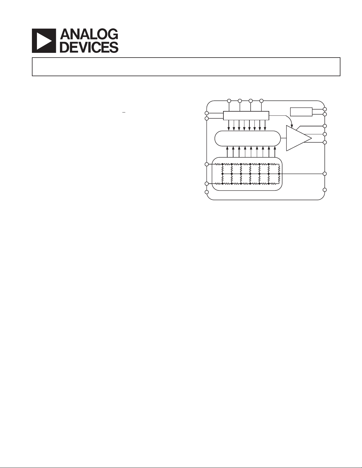
The signal input is applied to pins INHI and INLO. Variable gain
is achieved via two methods. The 6 dB gain steps are implemented
using a discrete X-AMP
®
structure, in which the input signal is
progressively attenuated by a 200 W R-2R ladder network that
also sets the input impedance; the 3 dB steps are implemented at
the output of the amplifier. This combination provides very
accurate 3 dB gain steps over a span of 45 dB. The output impedance is set by on-chip resistors across the differential output pins,
AD8369
*
FUNCTIONAL BLOCK DIAGRAM
BIT3 BIT0BIT2 BIT1
DENB
SENB
INHI
INLO
COMM
GAIN CODE DECODE
Gm CELLS
3dB STEP
BIAS
VPOS
PWUP
FILT
OPHI
OPLO
CMDC
COMM
OPHI and OPLO. The overall gain depends upon the source
and load impedances due to the resistive nature of the input and
output ports.
Digital control of the AD8369 is achieved using either a serial or
a parallel interface. The mode of digital control is selected by
connecting a single pin (SENB) to ground or the positive supply. Digital control pins can be driven with standard CMOS
logic levels.
The AD8369 may be powered on or off by a logic level applied
to the PWUP pin. For a logic high, the chip powers up rapidly
to its nominal quiescent current of 37 mA at 25ºC. When low,
the total dissipation drops to less than a few milliwatts.
The AD8369 is fabricated on an Analog Devices proprietary, high
performance 25 GHz silicon bipolar IC process and is available
in a 16-lead TSSOP package for the industrial temperature range
of –40∞C to +85∞C. A populated evaluation board is available.
*Patents Pending
REV. 0
Information furnished by Analog Devices is believed to be accurate and
reliable. However, no responsibility is assumed by Analog Devices for its
use, nor for any infringements of patents or other rights of third parties that
may result from its use. No license is granted by implication or otherwise
under any patent or patent rights of Analog Devices. Trademarks and
registered trademarks are the property of their respective companies.
One Technology Way, P.O. Box 9106, Norwood, MA 02062-9106, U.S.A.
Tel: 781/329-4700 www.analog.com
Fax: 781/326-8703 © 2002 Analog Devices, Inc. All rights reserved.
Page 2

(VS = 5 V, T = 25ⴗC, RS = 200 ⍀, RL = 1000 ⍀, Frequency = 70 MHz, at maximum gain,
AD8369–SPECIFICATIONS
unless otherwise noted.)
Parameter Conditions Min Typ Max Unit
OVERALL FUNCTION
Frequency Range 3 dB Bandwidth LF* 600 MHz
GAIN CONTROL INTERFACE
Voltage Gain Span 45 dB
Maximum Gain All bits high (1 1 1 1) 40 dB
Minimum Gain All bits low (0 0 0 0) –5 dB
Gain Step Size 3dB
Gain Step Accuracy
Over entire gain range, with respect to 3 dB step
± 0.05 dB
Gain Step Response Time Step = 3 dB, settling to 10% of final value 30 ns
INPUT STAGE
Input Resistance From INHI to INLO 200 W
From INHI to COMM, from INLO to COMM 100 W
Input Capacitance From INHI to INLO 0.1 pF
From INHI to COMM, from INLO to COMM 1.1 pF
Input Noise Spectral Density 2 nV/÷Hz
Input Common-Mode DC Voltage Measured at pin CMDC 1.7 V
Maximum Linear Input |V
INHI
– V
| at Minimum Gain 2.2 V
INLO
OUTPUT STAGE
Output Resistance From OPHI to OPLO 200 W
From OPHI to COMM, from OPLO to COMM 100 W
Output Capacitance From OPHI to OPLO 0.25 pF
From OPHI to COMM, from OPLO to COMM 1.5 pF
Common-Mode DC Voltage No input signal V
/2 V
S
Slew Rate Output step = 1 V 1200 V/ms
POWER INTERFACE
Supply Voltage 3.0 5.5 V
Quiescent Current PWUP high 37 42 mA
vs. Temperature –40∞C £ T
£ 85∞C52mA
A
Disable Current PWUP low 400 750 mA
vs. Temperature –40∞C £ TA £ 85∞C1mA
POWER UP INTERFACE Pin PWUP
Enable Threshold 1.0 V
Disable Threshold 2.2 V
Response Time Time delay following low to high transition 7 ms
on PWUP until output settles to within 10%
of final value
Input Bias Current PWUP = 5 V 160 mA
DIGITAL INTERFACE
Pins SENB, BIT0, BIT1, BIT2, BIT3,
and DENB
Low Condition 2.0 V
High Condition 3.0 V
Input Bias Current Low input 150 mA
Frequency = 10 MHz
Voltage Gain 40.5 dB
Gain Flatness Within ± 10 MHz of 10 MHz
+0.05* dB
Noise Figure 7.0 dB
Output IP3 f1 = 9.945 MHz, f2 = 10.550 MHz +22 dBV rms
+22 dBm
IMD
3
Harmonic Distortion Second-Order, V
f1 = 9.945 MHz, f2 = 10.550 MHz
V
– V
OPHI
Third-Order, V
= 1 V p-p composite –74 dBc
OPLO
OPHI
OPHI
– V
– V
= 1 V p-p –72 dBc
OPLO
= 1 V p-p –71 dBc
OPLO
P1dB For ± 1dB deviation from linear gain +3 dBV rms
+3 dBm
*The low frequency high-pass corner is determined by the capacitor on pin FILT, C
. See the Theory of Operation section for details.
FILT
REV. 0–2–
Page 3

SPECIFICATIONS (Continued)
AD8369
Parameter Conditions Min Typ Max Unit
Frequency = 70 MHz
Voltage Gain 40.5 dB
Gain Flatness Within ± 20 MHz of 70 MHz ± 0.1 dB
Noise Figure 7.0 dB
Output IP3 f1 = 69.3 MHz, f2 = 70.7 MHz +19.5 dBV rms
+19.5 dBm
IMD
3
Harmonic Distortion Second-Order, V
f1 = 69.3 MHz, f2 = 70.7 MHz
– V
V
OPHI
Third-Order, V
= 1 V p-p composite –69 dBc
OPLO
OPHI
OPHI
– V
– V
= 1 V p-p –68 dBc
OPLO
= 1 V p-p –64 dBc
OPLO
P1dB For ± 1dB deviation from linear gain +3 dBV rms
+3 dBm
Frequency = 140 MHz
Voltage Gain 40.0 dB
Gain Flatness Within ± 20 MHz of 140 MHz ± 0.10 dB
Noise Figure 7.0 dB
Output IP3 f1 = 139.55 MHz, f2 = 140.45 MHz +17 dBV rms
+17 dBm
IMD
3
Harmonic Distortion Second-Order, V
f1 = 139.55 MHz, f2 = 140.45 MHz
– V
V
OPHI
Third-Order, V
= 1 V p-p composite –64 dBc
OPLO
OPHI
OPHI
– V
– V
= 1 V p-p –63 dBc
OPLO
= 1 V p-p –55 dBc
OPLO
P1dB For ± 1 dB deviation from linear gain +3 dBV rms
+3 dBm
Frequency = 190 MHz
Voltage Gain 39.7 dB
Gain Flatness Within ± 20 MHz of 190 MHz ± 0.1 dB
Noise Figure 7.2 dB
Output IP3 f1 = 189.55 MHz, f2 = 190.45 MHz +15.5 dBV rms
+15.5 dBm
IMD
3
Harmonic Distortion Second-Order, V
f1 = 189.55 MHz, f2 = 190.45 MHz
– V
V
OPHI
Third-Order, V
= 1 V p-p composite –61 dBc
OPLO
OPHI
OPHI
– V
– V
= 1 V p-p –57 dBc
OPLO
= 1 V p-p –51 dBc
OPLO
P1dB For ± 1dB deviation from linear gain +2 dBV rms
+2 dBm
Frequency = 240 MHz
Voltage Gain 39.3 dB
Gain Flatness Within ± 20 MHz of 240 MHz ± 0.1 dB
Noise Figure 7.2 dB
Output IP3 f1 = 239.55 MHz, f2 = 240.45 MHz +14 dBV rms
+14 dBm
IMD
3
Harmonic Distortion Second-Order, V
f1 = 239.55 MHz, f2 = 240.45 MHz
V
– V
OPHI
Third-Order, V
= 1 V p-p composite –58 dBc
OPLO
OPHI
OPHI
– V
– V
= 1 V p-p –50 dBc
OPLO
= 1 V p-p –49 dBc
OPLO
P1dB For ± 1 dB deviation from linear gain +1.5 dBV rms
+1.5 dBm
Frequency = 320 MHz
Voltage Gain 39.0 dB
Gain Flatness Within ± 20 MHz of 320 MHz ± 0.15 dB
Noise Figure 7.4 dB
Output IP3 f1 = 319.55 MHz, f2 = 320.45 MHz +11.5 dBV rms
+11.5 dBm
IMD
3
Harmonic Distortion Second-Order, V
f1 = 319.55 MHz, f2 = 320.45 MHz
V
– V
OPHI
Third-Order, V
= 1 V p-p composite –53 dBc
OPLO
OPHI
OPHI
– V
– V
= 1 V p-p –47 dBc
OPLO
= 1 V p-p –49 dBc
OPLO
P1dB For ± 1 dB deviation from linear gain +1.0 dBV rms
+1.0 dBm
REV. 0
–3–
Page 4
AD8369
SPECIFICATIONS (Continued)
Parameter Conditions Min Typ Max Unit
Frequency = 380 MHz
Voltage Gain 38.5 dB
Gain Flatness Within ± 20 MHz of 380 MHz ± 0.15 dB
Noise Figure 7.8 dB
Output IP3 f1 = 379.55 MHz, f2 = 380.45 MHz +8.5 dBV rms
+8.5 dBm
IMD
3
Harmonic Distortion Second-Order, V
f1 = 379.55 MHz, f2 = 380.45 MHz,
V
– V
OPHI
Third-Order, V
= 1 V p-p composite –47 dBc
OPLO
OPHI
OPHI
– V
– V
= 1 V p-p –45 dBc
OPLO
= 1 V p-p –49 dBc
OPLO
P1dB For ± 1 dB deviation from linear gain +0.5 dBV rms
+0.5 dBm
Specifications subject to change without notice.
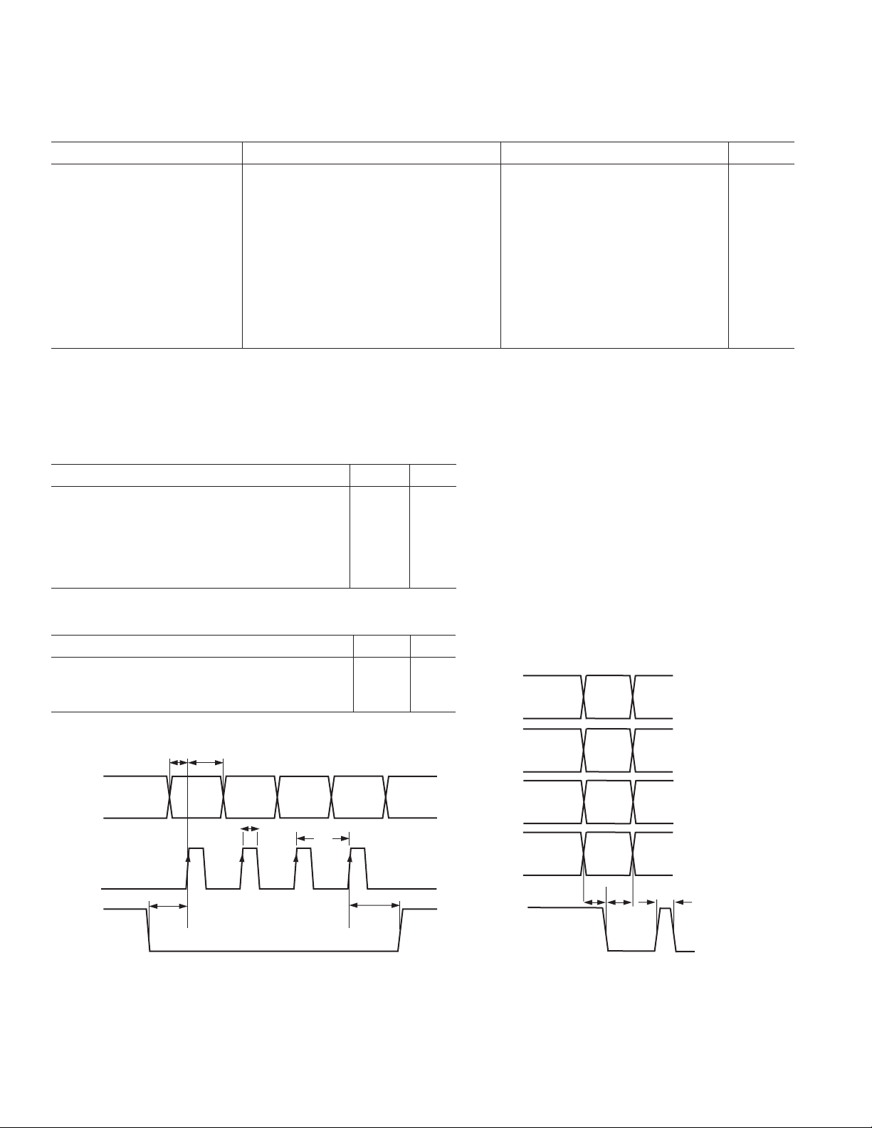
TIMING SPECIFICATIONS
SERIAL PROGRAMMING TIMING REQUIREMENTS
(VS = 5 V, T = 25∞C)
Parameter Typ Unit
Minimum Clock Pulsewidth (T
Minimum Clock Period (T
Minimum Setup Time Data vs. Clock (T
Minimum Setup Time Data Enable vs. Clock (T
Minimum Hold Time Clock vs. Data Enable (T
Minimum Hold Time Data vs. Clock (TDH)4ns
)10ns
PW
)20ns
CK
)2ns
DS
)2 ns
ES
)2 ns
EH
PARALLEL PROGRAMMING TIMING REQUIREMENTS
= 5 V, T = 25∞C)
(V
S
Parameter Typ Unit
Minimum Setup Time Data Enable vs. Data (T
Minimum Hold Time Data Enable vs. Data (T
Minimum Data Enable Width (TPW)4ns
T
T
DH
DS
DATA
(BIT 0)
CLOCK
(BIT 1)
DATA
ENABLE
(DEN B)
CLOCK
DISABLED
MSB MSB–1 MSB–2 LSB
T
PW
T
ES
DATA IS LATCHED ON LOW-TO-HIGH TRANSITION OF DENB
CLOCK
ENABLED
)2 ns
ES
)2 ns
EH
T
CK
T
EH
CLOCK
DISABLED
(NOT TO SCALE)
MSB
(BIT3)
MSB–1
(BIT2)
MSB–2
(BIT1)
LSB
(BIT0)
DENB
DATA IS LATCHED ON HIGH-TO-LOW
TRANSITION OF DENB
Serial Programming Timing
T
ESTEH
T
PW
(NOT TO SCALE)
Parallel Programming Timing
REV. 0–4–
Page 5
AD8369
ABSOLUTE MAXIMUM RATINGS*
Supply Voltage VS, VPOS . . . . . . . . . . . . . . . . . . . . . . . . 5.5 V
PWUP . . . . . . . . . . . . . . . . . . . . . . . . . . . . . . . . . V
BIT0, BIT1, BIT2, BIT3, DENB, SENB . . . . . . V
Input Voltage, V
Input Voltage, V
Input Voltage, V
INHI
INHI
INHI
– V
or V
– V
................................
. . . . . . . . . . . . . . . . . . . . . . . . 4 V
INLO
with respect to COMM . . 4.5 V
INLO
with respect to COMM
INLO
COMM – 200 mV
+ 200 mV
S
+ 200 mV
S
Internal Power Dissipation . . . . . . . . . . . . . . . . . . . . . 265 mW
. . . . . . . . . . . . . . . . . . . . . . . . . . . . . . . . . . . . . . . 150∞C/W
JA
Maximum Junction Temperature . . . . . . . . . . . . . . . . . 125∞C
Operating Temperature Range . . . . . . . . . . . .–40∞C to +85∞C
Storage Temperature Range . . . . . . . . . . . . . –65∞C to +150∞C
Lead Temperature Range (soldering 60 sec) . . . . . . . to 300∞C
*Stresses above those listed under Absolute Maximum Ratings may cause perma-
nent damage to the device. This is a stress rating only; functional operation of the
device at these or any other condition s above those indicated in the operational
section of this specification is not implied. Exposure to absolute maximum rating
conditions for extended periods may affect device reliability.
ORDERING GUIDE
Model Temperature Range Package Description Package Option
AD8369ARU –40ºC to +85ºC Tube, 16-Lead TSSOP RU-16
AD8369ARU-REEL7 –40ºC to +85ºC 7" Tape and Reel
AD8369EVAL Evaluation Board
Table I. Typical Voltage Gain vs. Gain Code (VS = 5 V, f = 70 MHz)
Typical Typical
Gain Gain (dB) Gain (dB)
Code BIT3 BIT2 BIT1 BIT0 RL = 1 k⍀ RL = 200 ⍀
00000–5 –10
10001–2 –7
200101 –4
300114 –1
401007 2
5010110 5
6011013 8
7011116 11
8100019 14
9100122 17
10 1 01025 20
11 1 01128 23
12 1 10031 26
13 1 10134 29
14 1 11037 32
15 1 11140 35
CAUTION
ESD (electrostatic discharge) sensitive device. Electrostatic charges as high as 4000 V readily
accumulate on the human body and test equipment and can discharge without detection. Although the
AD8369 features proprietary ESD protection circuitry, permanent damage may occur on devices
subjected to high energy electrostatic discharges. Therefore, proper ESD precautions are recommended
to avoid performance degradation or loss of functionality.
REV. 0
–5–
Page 6
AD8369
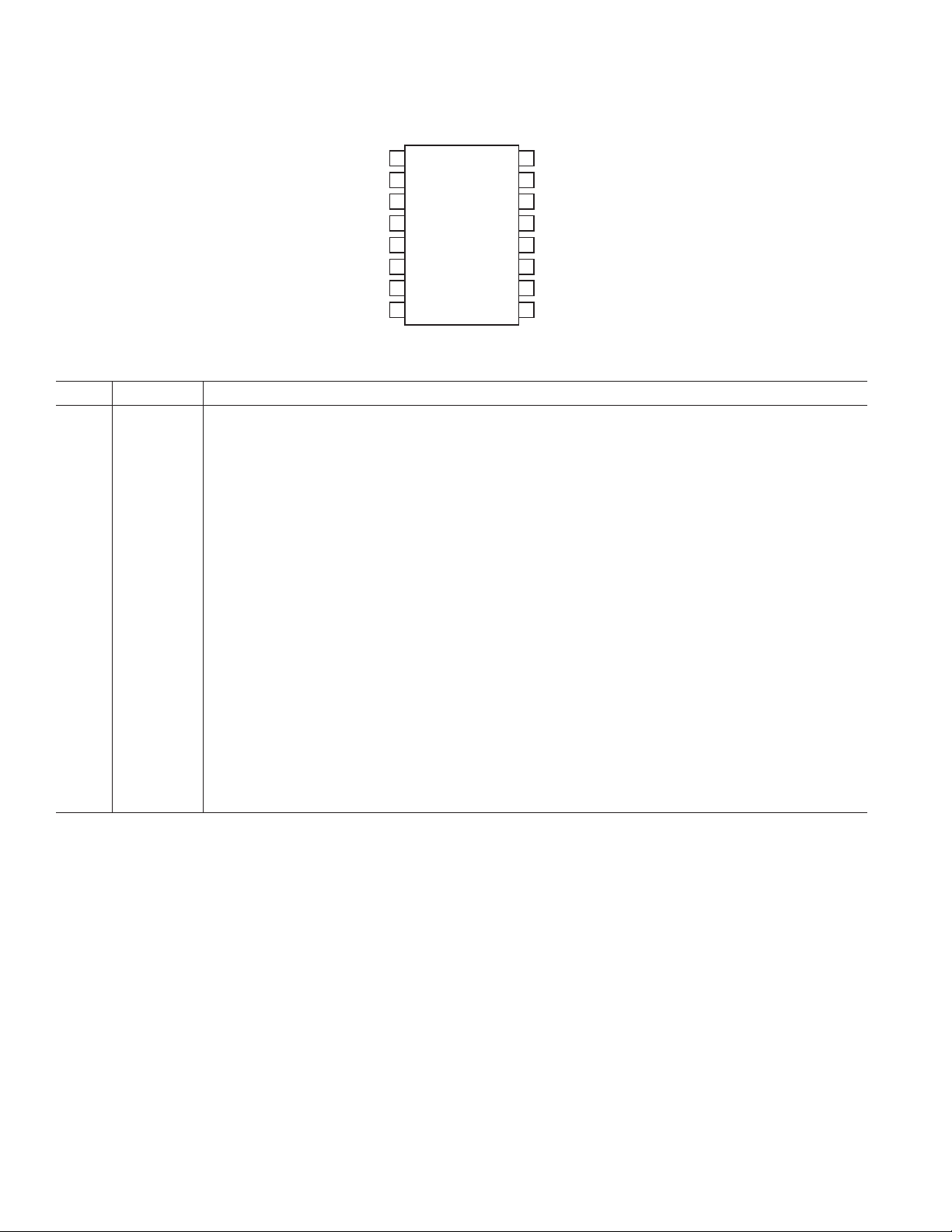
PIN CONFIGURATION
16
INLO
1
2
COMM
AD8369
3
BIT0
BIT1
BIT2
BIT3
DENB
OPLO OPHI
4
5
6
7
8
TOP VIEW
(Not To Scale)
PIN FUNCTION DESCRIPTIONS
Pin No. Mnemonic Function
1 INLO Balanced Differential Input. Internally biased, should be ac-coupled.
2 COMM Device Common. Connect to low impedance ground.
3 BIT0 Gain Selection Least Significant Bit. Used as DATA input signal when in serial mode of operation.
4 BIT1 Gain Selection Control Bit. Used as CLOCK input pin when in serial mode of operation.
5 BIT2 Gain Selection Control Bit. Inactive when in serial mode of operation.
6 BIT3 Gain Selection Most Significant Bit. Inactive when in serial mode of operation.
7 DENB Data Enable Pin. Writes data to register. See Timing Specifications for details.
8 OPLO Balanced Differential Output. Biased to midsupply, should be ac-coupled.
9 OPHI Balanced Differential Output. Biased to midsupply, should be ac-coupled.
10 CMDC Common-Mode Decoupling Pin. Connect bypass capacitor to ground for additional common-mode supply
decoupling beyond the existing internal decoupling.
11 FILT High-Pass Filter Connection. Used to set high-pass corner frequency.
12 SENB Serial or Parallel Interface Select. Connect SENB to VPOS for serial operation. Connect SENB to COMM
for parallel operation.
13 VPOS Positive Supply Voltage, V
= +3 V to +5.5 V.
S
14 PWUP Power-Up Pin. Connect PWUP to VPOS to power up the device. Connect PWUP to COMM to power-down.
15 COMM Device Common. Connect to a low impedance ground.
16 INHI Balanced Differential Input. Internally biased, should be ac-coupled.
INHI
15
COMM
14
PWUP
13
VPOS
12
SENB
11
FILT
10
CMDC
9
REV. 0–6–
Page 7
Typical Performance Characteristics–AD8369
FREQUENCY – MHz
10
OUTPUT IP3 – dBm
100 1000
35
30
25
20
10
0
15
5
OUTPUT IP3 – dBV rms
28
23
18
13
3
–7
8
–2
(VS = 5 V, T = 25ⴗC, RS = 200 ⍀, Maximum gain, unless otherwise noted.)
50
40
30
20
10
GAIN – dB
0
ⴚ10
ⴚ20
01
23456 78 910
RL = 1k⍀
GAIN CODE
TPC 1. Gain vs. Gain Code at 70 MHz
43
41
39
37
35
33
GAIN – dB
31
29
27
25
10
VS = 3V, RL = 1k⍀
VS = 3V, RL = 200⍀
FREQUENCY – MHz
VS = 5V, RL = 1k⍀
VS = 5V, RL = 200⍀
100 1000
RL = 200⍀
11 12 13 14 15
50
40
30
20
10
GAIN – dB
0
ⴚ10
ⴚ20
10
FREQUENCY – MHz
GAIN CODE 15
GAIN CODE 0
100 1000
TPC 4. Gain vs. Frequency by Gain Code, RL = 1 k
50
40
30
20
10
GAIN – dB
0
ⴚ10
ⴚ20
10
FREQUENCY – MHz
GAIN CODE 15
GAIN CODE 0
100 1000
W
TPC 2. Maximum Gain vs. Frequency by RL and
Supply Voltage
28
26
24
22
OUTPUT IP3 – dBm
18
16
14
23456 78 9102011 12 13 14 15
01
GAIN CODE
TPC 3. Output IP3 vs. Gain Code at 70 MHz, VS = 5 V,
= 200
R
L
W
REV. 0 –7–
21
19
17
15
13
11
OUTPUT IP3 – dBV rms
9
7
TPC 5. Gain vs. Frequency by Gain Code, RL = 200
TPC 6. Output IP3 vs. Frequency, VS = 5 V, RL = 200
Maximum Gain
W
W
Page 8
AD8369
–63
–64
–65
–66
–67
OUTPUT IMD – dBc
–68
–69
–70
4
0
3215678
GAIN CODE
91011121314 15
TPC 7. Two-Tone, IMD3 vs. Gain Code at 70 MHz,
V
OPHI
ⴚ40
ⴚ45
ⴚ50
ⴚ55
ⴚ60
– V
= 1 V p-p, VS = 5 V, RL = 1 k
OPLO
HD
3
HD
2
W
–20
–30
–40
–50
–60
OUTPUT IMD – dBc
–70
–80
0
200
15010050 250 300 350 400
FREQUENCY – MHz
TPC 10. Two-Tone IMD3 vs. Frequency V
VS = 5 V, RL = 1 kW, Maximum Gain
ⴚ35
ⴚ40
ⴚ45
ⴚ50
ⴚ55
HD
3
HD
2
450 500 550 600
– V
OPHI
OPLO
= 1 V p-p,
ⴚ65
HARMONIC DISTORTION – dBc
ⴚ70
ⴚ75
050
TPC 8. Harmonic Distortion at V
Frequency, V
50
40
30
20
NOISE FIGURE – dB
10
0
01
100 150 200 250 300 350 400
FREQUENCY – MHz
– V
= 5 V, RL = 1 kW, Maximum Gain
S
23456 78 910
OPHI
GAIN CODE
OPLO
11 12 13 14 15
= 1 V p-p vs.
TPC 9. Noise Figure vs. Gain Code at 70 MHz, VS = 5 V,
= 200
R
L
W
ⴚ60
HARMONIC DISTORTION – dBc
ⴚ65
ⴚ70
050
TPC 11. Harmonic Distortion at V
Frequency, V
8.0
7.8
7.6
7.4
7.2
NOISE FIGURE – dB
7.0
6.8
6.6
050
100 150 200 250 300 350 400
FREQUENCY – MHz
– V
= 5 V, RL = 200 W, Maximum Gain
S
RL = 1k⍀
100 150 200 250 300 350 400
FREQUENCY – MHz
OPHI
5V
3V
RL = 200⍀
TPC 12. Noise Figure vs. Frequency by RL and
Supply Voltage at Maximum Gain
= 1 V p-p vs.
OPLO
REV. 0–8–
Page 9

AD8369
FREQUENCY – MHz
10
P1dB – dBm
100 1000
0
1
2
3
4
5
6
7
8
9
P1dB – dBV rms
–7
–6
–5
–4
–3
–2
–1
0
1
2
9.0
8.5
8.0
7.5
7.0
6.5
6.0
P1dB – dBm
5.5
5.0
4.5
4.0
01
23456 78 91011 12 13 14 15
GAIN CODE
TPC 13. Output P1dB vs. Gain Code at 70 MHz,
= 5 V, RL = 200
V
S
80
70
60
50
40
CMRR – dB
30
20
10
W
2.0
1.5
1.0
0.5
0
–0.5
–1.0
P1dB – dBV rms
–1.5
–2.0
–2.5
–3.0
TPC 16. Output P1dB vs. Frequency, VS = 5 V,
= 200 W, Maximum Gain
R
L
ⴚ40
ⴚ50
ⴚ60
ⴚ70
ⴚ80
REVERSE ISOLATION – dB
ⴚ90
0
10
100 1000
FREQUENCY – MHz
TPC 14. Common-Mode Rejection Ratio vs. Frequency
at Maximum Gain, V
= 5 V, RL = 200 W (Refer to
S
Appendix for Definition)
250
R
200
RESISTANCE – ⍀
150
100
10
TPC 15. Equivalent Input Resistance and
Capacitance vs. Frequency at Maximum Gain
REV. 0
INHI
INLO
FREQUENCY – MHz
100
C
1000
0.75
0.50
0.25
0
CAPACITANCE – pF
–9–
ⴚ100
10
100 1000
FREQUENCY – MHz
TPC 17. Reverse Isolation vs. Frequency at
Maximum Gain, V
= 5 V, RL = 200 W (Refer to
S
Appendix for Definition)
250
200
⍀
RESISTANCE –
150
100
10
OPHI
OPLO
FREQUENCY – MHz
R
C
100
TPC 18. Equivalent Output Resistance and
Capacitance vs. Frequency at Maximum Gain
1000
0.75
0.50
0.25
0
CAPACITANCE – pF
Page 10

AD8369
90
GAIN
15
60
10MHz
380MHz
500MHz
300
30
0
330
180
150
210
120
GAIN CODES
0, 1, AND 9
240
CODE
750MHz
270
TPC 19. Differential Input Reflection Coefficient,
S
, ZO = 50 W Differential, Selected Gain Codes
11
DIFFERENTIAL OUTPUT
250mV/VERTICAL DIVISION
ZERO
AVERAGE OF 128 SAMPLES
90
GAIN
CODE
15
500MHz
60
30
10MHz
0
380MHz
330
300
180
150
210
120
GAIN CODES
0, 1, AND 9
240
750MHz
270
TPC 22. Differential Output Reflection Coefficient,
S
, ZO = 50 W Differential, Selected Gain Codes
22
INPUT = 250mV p-p, 10MHz
OVERDRIVE
ZERO
OUTPUT
1V/VERTICAL
DIVISION
RECOVERY
BIT 0
2V/VERTICAL DIVISION
GND
TIME – 20ns/DIV
TPC 20. Gain Step Time Domain Response, 3 dB Step,
VS = 5 V, RL = 1 kW, Parallel Transparent Mode
DIFFERENTIAL OUTPUT
ZERO
GND
70MHz, 750mV/DIV
PWUP 2V/VERTICAL DIVISION
TIME – 2s/DIV
TPC 21. PWUP Time Domain Response,
Maximum Gain, V
= 5 V, RL = 1 k
S
W
BIT 3
2V/VERTICAL DIVISION
GND
TIME – 1s/DIV
TPC 23. Overdrive Recovery, Maximum Gain,
VS = 5 V, RL = 1 kW, Parallel Transparent Mode
DIFFERENTIAL
OUTPUT
ZERO
GND
TIME – 20s/DIV
200mV/DIV
INPUT
2mV/DIV
TPC 24. Pulse Response, Maximum Gain, VS = 5 V,
= 1 k
R
W
L
REV. 0–10–
Page 11

2.0
FREQUENCY – MHz
10
GAIN ERROR – dB
100 1000
0.5
0
1.0
1.5
2.0
ⴚ0.5
ⴚ1.0
ⴚ1.5
ⴚ2.0
ⴚ40ⴗC
ⴙ85ⴗC
GAIN ERROR AT ⴚ40ⴗC AND ⴙ85ⴗC
WITH RESPECT TO ⴙ25ⴗC. DATA BASED
ON 45 PARTS FROM TWO BATCH LOTS.
FREQUENCY – MHz
10
GAIN ERROR – dB
100 1000
0.5
0
1.0
1.5
2.0
ⴚ0.5
ⴚ1.0
ⴚ1.5
ⴚ2.0
GAIN ERROR AT ⴚ40ⴗC AND ⴙ85ⴗC
WITH RESPECT TO ⴙ25ⴗC. DATA BASED
ON 45 PARTS FROM TWO BATCH LOTS.
ⴚ40ⴗC
ⴙ85ⴗC
FREQUENCY – MHz
10
P1dB – dBm
100 1000
0
6
10
–2
2
4
8
ⴙ85ⴗC
ⴚ40ⴗC
ⴙ25ⴗC
P1dB – dBV rms
–7
–1
3
–9
–5
–3
1
1.5
1.0
AD8369
0.5
0
ⴚ0.5
GAIN ERROR – dB
ⴚ1.0
GAIN ERROR AT ⴚ40ⴗC AND ⴙ85ⴗC
ⴚ1.5
WITH RESPECT TO ⴙ25ⴗC. DATA BASED
ON 45 PARTS FROM TWO BATCH LOTS.
ⴚ2.0
10
FREQUENCY – MHz
ⴚ40ⴗC
ⴙ85ⴗC
100 1000
TPC 25. Gain Error Due to Temperature Change vs.
Frequency, 3 Sigma to Either Side of Mean, V
= 5 V,
S
RL = 1 kW, Maximum Gain
2.0
1.5
1.0
0.5
0
ⴚ0.5
GAIN ERROR – dB
ⴚ1.0
GAIN ERROR AT ⴚ40ⴗC AND ⴙ85ⴗC
ⴚ1.5
WITH RESPECT TO ⴙ25ⴗC. DATA BASED
ON 45 PARTS FROM TWO BATCH LOTS.
ⴚ2.0
10
FREQUENCY – MHz
ⴚ40ⴗC
ⴙ85ⴗC
100 1000
TPC 28. Gain Error Due to Temperature Change
vs. Frequency, 3 Sigma to Either Side of Mean,
V
= 5 V, RL = 200 W, Maximum Gain
S
TPC 26. Gain Error Due to Temperature Change vs.
Frequency, 3 Sigma to Either Side of Mean, V
RL = 1 kW, Maximum Gain
35
30
25
20
15
OUTPUT IP3 – dBm
10
TPC 27. IP3 vs. Frequency by Temperature, VS = 5 V,
RL = 200 W, Maximum Gain
REV. 0
–40ⴗC
+85ⴗC
FREQUENCY – MHz
5
0
10
100
+25ⴗC
= 3 V,
S
1000
28
23
18
13
8
OUTPUT IP3 – dBV rms
3
–2
–7
–11–
TPC 29. Gain Error Due to Temperature Change
vs. Frequency, 3 Sigma to Either Side of Mean,
= 3 V, RL = 200 W, Maximum Gain
V
S
TPC 30. Output P1dB vs. Frequency by Temperature,
VS = 5 V, RL = 200 W, Maximum Gain
Page 12

AD8369
60
50
40
30
PA RT COUNT
20
10
0
3.06
3.08
GAIN STEP SIZE – dB/CODE
3.10 3.12 3.14
SAMPLE FROM
ONE BATCH LOT
TPC 31. Distribution of Gain Step Size, 70 MHz,
V
= 5 V
S
18
16
14
12
10
8
PA RT COUNT
6
4
2
0
–73 –72 –71 –70 –69 –68 –67 –66 –65 –64 –63 –62
–74
IMD – dBc
SAMPLE FROM
TWO BATCH LOTS
TPC 32. Distribution of IMD3, 70 MHz, RL = 1 kW,
V
OPHI
– V
= 1 V p-p Composite, VS = 5 V,
OPLO
Maximum Gain
40
35
30
25
20
PA RT COUNT
15
10
5
0
3.16
3.18 3.20 3.22
GAIN STEP SIZE – dB/CODE
SAMPLE FROM
ONE BATCH LOT
TPC 34. Distribution of Gain Step Size, 320 MHz,
V
= 5 V
S
26
24
22
20
18
16
14
12
10
PA RT COUNT
8
6
4
2
0
–58
–57 –56
–53 –52–55 –54 –51 –50 –49 –48
IMD – dBc
SAMPLE FROM
TWO BATCH LOTS
TPC 35. Distribution of IMD3, 320 MHz, RL = 1 kW,
V
OPHI
– V
= 1 V p-p Composite, VS = 5 V,
OPLO
Maximum Gain
3000
2500
2000
1500
1000
GROUP DELAY – ps
500
0
0
3V, RL = 1k⍀
5V, RL = 1k⍀
3V, RL = 200⍀
5V, RL = 200⍀
400
300200100 500 600 700 800
FREQUENCY – MHz
TPC 33. Group Delay vs. Frequency by RL and
Supply Voltage at Maximum Gain
1600
1400
1200
1000
800
GROUP DELAY – ps
600
400
0
100 200 300 400 500 600 700 800
FREQUENCY – MHz
ALL GAIN CODES
REPRESENTED
TPC 36. Group Delay vs. Frequency by Gain Code,
VS = 5 V, RL = 1 kW, Maximum Gain
REV. 0–12–
Page 13

DIGITAL
INHI
CMDC
INLO
100
90
80
70
60
50
40
PSSR – dB
30
20
10
0
10
100 1000
FREQUENCY – kHz
TPC 37. Power Supply Rejection Ratio, VS = 5 V,
R
= 1 kW, Maximum Gain
L
GAIN STEP SELECTION
Gm CELLS
~
FIXED
GAIN
V
S
2
– 0.7
20pF
3dB SWITCHED
ATTENUATOR
BIAS
10000
AD8369
V
S
OPHI
100⍀
V
/2
S
V
S
100⍀
V
/2
S
OPLO
22pF
Figure 1. General Block Diagram, Control and Signal Paths Are Differential
THEORY OF OPERATION
The AD8369 is a digitally controlled fully differential VGA
based on a variation of Analog Devices’ patented X-AMP architecture (Figure 1). It provides accurate gain control over a 45 dB
span with a constant –3 dB bandwidth of 600 MHz.
The 3 dB gain steps can be controlled by a user-selectable
parallel- or serial-mode digital interface. A single pin (SENB)
selects the mode. The AD8369 is designed for optimal
operation when used in a fully differential system, although
single-ended operation is also possible. Its nominal input and
output impedances are 200 W.
Input Attenuator and Output 3 dB Step
The AD8369 is comprised of a seven-stage R-2R ladder network (eight taps) and a selected Gm stage followed by a
fixed-gain differential amplifier. The ladder provides a total
attenuation of 42 dB in 6 dB steps. The full signal is applied to
amplifier using the first tap; at the second tap, the signal
the
is 6 dB lower and so on. A further 3dB interpolating gain step is
introduced at the output of the fixed gain amplifier, providing
the full 45 dB of gain span.
Fixed Gain Amplifier
The fixed gain amplifier is driven by the tap point of the R-2R
ladder network via the selected Gm cell. The output stage is a
complementary pair of current sources, loaded with internal
100 W resistors to ac ground which provides a 200 W differential
output impedance. The low frequency gain of the AD8369
can be approximated by the equation:
V
OUT L
V
IN
06
.
Ê
Á
Ë
200
200
Ê
ˆ
R
Á
˜
Á
R=+
¯
L
Ë
ˆ
1
˜
˜
-
15
n
()
¯
2
where RL is the external load resistor in ohms and n is the gain
code; 0 is the minimum gain code and 15 is the maximum gain
code. The external load, which is in parallel combination with
the internal 200 W output resistor, affects the overall gain and
peak output swing. Note that the external load has no effect on the
gain step size.
Input and Output Interfaces
The dc working points of the differential input and output interfaces of the AD8369 are internally biased. The inputs INHI and
INLO are biased to a diode drop below V
/2 (~1.7 V for a 5 V
S
positive supply) to meet isolation and headroom constraints,
while the outputs OPHI and OPLO are centered on the supply
midpoint, V
/2, to provide the maximum output swing.
S
The internal VS/2 reference and the CMDC reference are buffered and decoupled to ground via internal capacitors. The
input bias voltage, derived from this VS/2 reference, is brought
REV. 0
–13–
Page 14

AD8369
DENB
SENB
B A
MUX
B A
MUX
B A
MUX
B A
MUX
SHIFT
REGISTER
A/B
SHIFT
REGISTER
SHIFT
REGISTER
SHIFT
REGISTER
BIT0
(DATA)
BIT1
(CLOCK)
BIT2 BIT3
GAIN CONTROL REGISTER
(LATCH)
TO GAIN CONTROL SECTION
BIT0 BIT1 BIT2 BIT3
T/H
out to pin CMDC for decoupling to ground. An external
capacitor from CMDC to COMM of 0.01 mF or more is
recommended to lower the input common-mode impedance of
the AD8369 and improve single-ended operation.
Signals must be ac-coupled at the input, either via a pair of
capacitors or a transformer. These may not be needed when the
source has no dc path to ground, such as a SAW filter. The
output may need dc blocking capacitors when driving dcgrounded loads, but it can be directly coupled to an ADC,
provided that the common-mode levels are compatible.
The input and output resistances form a high-pass filter in combination with any external ac-coupling capacitors that should
be chosen to minimize signal roll-off at low frequencies. For
example, using input-coupling capacitors of 0.1 mF, each driving
a 100 W input node (200 W differential), the –3 dB high-pass
corner frequency is at:
p()()
210 100
It is important to note that the input and output resistances are
subject to process variations of up to ± 20%. This will affect the
high-pass corner frequencies and the overall gain when driven
from, or loaded by, a finite impedance (see the Reducing Gain
Sensitivity to Input and Output Impedance Variation section).
Noise and Distortion
It is a common aspect of this style of VGAs, however implemented, that the effective noise figure worsens as the gain is
reduced. The AD8369 uses a fixed gain amplifier, having a certain
invariant noise spectral density, preceded by an attenuator.
Thus, the noise figure increases simply by 6 dB per tap point,
from a starting point of 7 dB at full gain.
However, unlike voltage-controlled amplifiers that must necessarily invoke nonlinear elements in the signal path, the distortion
in a step-gain amplifier can be very low and is essentially independent of the gain setting. Note that the postamplifier 3 dB step
does not affect the noise performance, but it has some bearing
on the output third-order intercept (OIP3). See TPCs 3 and 9.
Offset Control Loop
The AD8369 uses a control loop to null offsets at the input. If
left uncorrected, these offsets, in conjunction with the gain of
the AD8369, would reduce the available voltage swing at the
output. The control loop samples the differential output voltage error and feeds nulling currents back into the input stage.
The nominal high-pass corner frequency of this loop is internally set to 520 kHz, but it is subject to process variations of
up to ± 20%. This corner frequency can be reduced by adding
an external capacitor from the FILT pin to ground, in parallel
to an internal 30 pF capacitor. For example, an external capacitor of 0.1 mF would lower the high-pass corner by a factor of
30/100,030, to approximately 156 Hz. This frequency
be chosen to be at least one decade below the lowest component of interest in the input spectrum.
Digital Control
The gain of the AD8369 is controlled via a serial or parallel
interface, as shown in Figure 2. Serial or parallel operation is
selected via the SENB pin. Setting SENB to a logic low (< V
selects parallel operation, while a logic high on SENB (> V
selects serial operation. The AD8369 has two control registers, the
gain control register and the shift register. The gain control register
is a latch that holds the data that sets the amplifier gain. The
shift registers are composed of four flip-flops that accept the
serial data stream.
1
7
–
= kHz
16
Figure 2. Digital Interface Block Diagram
In parallel operation, the 4-bit parallel data is placed on pins
BIT3 through BIT0 and passed along to the gain control register
via the mux. Data is latched into the gain control register on the
falling edge of the input to DENB, subject to meeting the specified setup and hold times. If this pin is held high (> V
/2), any
S
changes in the parallel data will result in a change in the gain,
after propagation delays. This is referred to as the transparent
mode of operation. If DENB is held low, the last 4-bit word in
the gain control register will remain latched regardless of the signals
at the data inputs.
In serial operation, the BIT0 pin is used for data input while the
BIT1 pin is the clock input. Data is loaded into the serial shift
registers on the rising edge of the clock when DENB is low.
Given the required setup and hold times are observed, four rising
edge transitions of the clock will fully load the shift register. On
the rising edge of DENB, the 4-bit word in the shift register is
passed into the gain control register. While this pin is held high,
the clock input to the shift registers is turned off. Once DENB is
taken low, the shift register clock is again enabled and the last 4-bit
word prior to enabling the clock will be latched into the gain
control registers. This enables the loading of a new 4-bit gain
control word without interruption of the signal path. Only when
DENB goes high is data transferred from the shift registers to the
gain control registers. If no connections are made to the digital
control pins, internal 40 kW resistors pull these pins to levels
that set the AD8369 to its minimum gain condition.
At power-up or chip enable, if the AD8369 is in parallel mode
and DENB is held low, the gain control register will come up in
an indeterminate state. To avoid this, DENB should be held
high with valid data present during power-up when operating in
should
the parallel mode. In serial mode, the data in the gain control
interface powers up with a random gain code independent of
S
/2)
S
the DENB pin. Serial mode operation requires at least four
clock cycles and the transition of DENB from low to high for
/2)
valid data to be present at the gain control register.
REV. 0–14–
Page 15

AD8369
V
S
3V TO 5.5V
0.1F
INⴙ
50⍀ TX LINE
TC4-1W
0.1F
0.1F
PWUP VPOS SENB FILT CMDC OPHI
COMM
INHI
R
L
INLO DENBCOMM BIT0 BIT1 BIT2 BIT3
Figure 3. Basic Connections
BASIC CONNECTIONS
Figure 3 shows the minimum connections required for basic
operation of the AD8369. Supply voltages of between +3 V and
+5.5 V are permissible. The supply to the VPOS pin should be
decoupled with at least one low inductance surface-mount ceramic
capacitor of 0.1 mF placed as close as possible to the device. More
effective decoupling is provided by placing a 100 pF capacitor in
parallel and including a 4.7 W resistor in series with the supply.
Attention should be paid to voltage drops. A ferrite bead is a
better choice than the resistor where a smaller drop is required.
Input-Output Interface
A broadband 50 W input termination can be achieved by
using a 1:2 turns-ratio transformer, as shown in Figure 3.
This also can be used to convert a single-ended input signal
to a balanced differential form at the inputs of the AD8369.
As in all high frequency applications, the trace impedance
should be maintained right up to the input pins by careful
design of the PC board traces, as described in the PCB
Layout Considerations section.
Reducing Gain Sensitivity to Input and Output Impedance Variation
The lot-to-lot variations in gain mentioned previously can, in
principle, be eliminated by adjustments to the source and load.
Define a term as a function of the input and output resistances
of the AD8369 and the source and load resistances presented to it:
RR
RR
=
a
SOURCE INPUT
OUTPUT LOAD
()
=
a
()
0.1F
0.1F
0.1F
910111213141516
R
AD8369
OPLO
87654321
0.1F
CONTROL INTERFACE
L
In general, there is a loss factor, 1/(1+ ), at each interface so
the
overall gain reduction due to source and output loading is
40 log10 (1 + ). In this case, the input and output loss factors
are 0.8 (1.94 dB) at each interface so the overall gain is
reduced by 3.88 dB.
Operation from a Single-Sided Source
While there are distinct benefits of driving the AD8369 with a
well-balanced input, in terms of distortion and gain conformance at high frequencies, satisfactory operation will often be
possible when a single-sided source is ac-coupled directly to pin
INHI, and pin INLO is ac-grounded via a second capacitor. This
mode of operation takes advantage of the good HF common-mode
rejection of the input system. The capacitor values are, as always,
selected to ensure adequate transmission at low frequencies.
0.1F
0.1F
OPLO
0.1F
910111213141516
R
L
87654321
0.1F
50⍀
SOURCE
V
S
0.1F
0.1F
PWUP VPOS SENB FILT CMDC OPHI
COMM
INHI
AD8369
INLO DENBCOMM BIT0 BIT1 BIT2 BIT3
0.1F
For a 50 W source, = 0.25. Then the load resistance for zero
sensitivity to variations must be 800 W. Put more simply:
RRRR
()()
SOURCE LOAD INPUT OUTPUT
=
()( )
= 200
2
REV. 0
CONTROL INTERFACE
Figure 4. Single-Ended-to-Differential Application Example
–15–
Page 16

AD8369
For example, suppose the input signal in Figure 4 is a 140 MHz
sinusoid from a ground-referenced 50 W source. The 0.1 mF
coupling capacitors present a very low reactance at this frequency
(11 mW) so that essentially all of the ac voltage is delivered to the
differential inputs of the AD8369. It will be apparent that, in
addition to the use of adequate coupling capacitance, the external
capacitor used to extend the low frequency range of the offset
control loop, C
, must also be large enough to prevent the
FILT
offset control loop from attempting to track the ac signal fluctuations.
V
S
0.1F
PWUP VPOS SENB FILT CMDC OPHI
COMM
INHI
AD8369
INLO DENBCOMM BIT0 BIT1 BIT2 BIT3
0.1F
0.1F
OPLO
CONTROL INTERFACE
Figure 5. AD8369 to ADC Interface
0
–10
–20
–30
–40
–50
– dBFS
OUT
–60
P
–70
–80
–90
–100
51015202530
0
ADC OUTPUT FREQUENCY – MHz
70MHz – 1dBFS
HD2 = –83dBc
HD3 = –80dBc
SNR = 51dB
Figure 6. Single-Tone 70 MHz, –1 dBFS
0
–10
–20
–30
–40
–50
– dBFS
OUT
–60
P
–70
–80
–90
–100
0
–7dBFS
–72.5dBFS
51015202530
ADC OUTPUT FREQUENCY – MHz
Interfacing to an ADC
The AD8369 can be used to effectively increase the dynamic
range of an ADC in a direct IF sampling receiver application.
Figure 5 provides an example of an interface to an ADC designed
for an IF of 70 MHz. It comprises a low-pass filter that attenuates
harmonics while providing an impedance transformation from
200 W to 1 kW. This impedance transformation allows the AD8369
to operate much below its peak output swing in the pass band,
which significantly reduces distortion.
270nH
0.1F
910111213141516
6.8pF 15pF
87654321
0.1F
270nH
ADC
1k⍀
A high performance 14-bit ADC, the AD6645, is used for illustrative purposes and is sampling at 64 MSPs with a full-scale
input of 2.2 V p-p. Typically, an SNR of 51 dB and an SFDR of
almost –90 dBFS are realized by this configuration. Figure 6 shows
an FFT of the AD8369 delivering a single tone at –1 dBFS (that
is, 2 V p-p) at the input of the ADC with an HD2 of –83 dBc and
HD3 of –80 dBc. Figure 7 shows that the two-tone, third-order
intermodulation distortion level is –65.5 dBc.
PCB Layout Considerations
Each input and output pin of the AD8369 presents 100 W
rela
tive to their respective ac grounds. To ensure that signal
integrity is not seriously impaired by the printed circuit board, the
relevant connection traces should provide a characteristic
impedance of 100 W to the ground plane. This can be achieved
through proper layout. Figure 8 shows the cross section of a PC
board and Table II shows the dimensions that will provide a
100 W line impedance.
Table II. Dimensions Required for 100 W Characteristic
Impedance Microstrip Line in FR-4
(FR-4) 4.6
r
W22 mils
H53 mils
T 2.1 mils
Figure 7. Two-Tone, 70 MHz, 70.3 MHz, –7 dBFS
REV. 0–16–
Page 17

AD8369
Key considerations when laying out an RF trace with a controlled
impedance include:
•
Space the ground plane to either side of the signal trace at least
3 line-widths away to ensure that a microstrip (vertical dielectric) line is formed, rather than a coplanar (lateral dielectric)
waveguide.
•
Ensure that the width of the microstrip line is constant and
that there are as few discontinuations (component pads, etc.)
as possible along the length of the line. Width variations
cause impedance discontinuities in the line and may result
in unwanted reflections.
•
Do not use silkscreen over the signal line; this will alter the
line impedance.
•
Keep the length of the input and output connection lines as
short as possible.
SW 2
PWDN
13
2
C5
0.1F
PWUP VPOS SENB FILT CMDC OPHI
COMM
L
C8
1nF
AD8369
R60⍀R70⍀R80⍀R90⍀R10
INⴙ
INⴚ
J1
J2
LATCH
TC4-1W
0⍀
PWUP
V
S
C4
1nF
INHI
T1
R2
0⍀
R1
R
INLO DENBCOMM BIT0 BIT1 BIT2 BIT3
1nF
C3
3W 3WW
T
H
⑀
r
Figure 8. Cross-Sectional View of a PC Board
The AD8369 contains both digital and analog sections. Care
should be taken to ensure that the digital and analog sections
are adequately isolated on the PC board. The use of separate
ground planes for each section connected at only one point via a
ferrite bead inductor will ensure that the digital pulses do not
adversely affect the analog section of the AD8369.
R5
OPEN
C7
C8
0.1F
1nF
0⍀
910111213141516
OPLO
87654321
C2
1nF
1nF
C1
R11
0⍀
T2
TC4-1W
R12
0⍀
OUTⴙ
J6
OUTⴚ
J7
REV. 0
CLOCK
DATA
C9
OPEN
R3
1k⍀
31012498761152 131
15 22 2416 21201918 231714 25
R13
1k⍀
R4
1k⍀
D-SUB 25 PIN MALE
25 8 11
1
3467 10912
Figure 9. Evaluation Board Schematic
–17–
SW3
V
SW4
14
28
4
S
V
S
A
3
2
SW1
B
1
Page 18

AD8369
Evaluation Board
The evaluation board allows for quick testing of the AD8369
using standard 50 W test equipment. The schematic is shown in
Figure 9. Transformers T1 and T2 are used to transform 50 W
source and load impedances to the desired 200 W reference level.
This allows for broadband operation of the device without the need
to pay close attention to impedance matching (see Table III).
Evaluation Board Software
The evaluation board comes with the AD8369 control software
that allows for serial gain control from most computers. The
evaluation board is connected via a cable to the parallel port of
the computer. By simply adjusting the slider bar in the control
software, the gain code is automatically updated to the AD8369.
On some older PCs, it may be necessary to use 5 kW pull-up
resistors to VPOS on DATA, CLOCK, and LATCH depending
upon the capabilities of the port transceiver.
It is necessary to set SW3 on the evaluation board to “SER” for
the control software to function normally.
A screen shot of the evaluation software interface is shown in
Figure 11.
Figure 10. Evaluation Board Layout
Figure 11. Evaluation Software Interface
REV. 0–18–
Page 19

AD8369
Table III. AD8369 Evaluation Board Configuration Options
Component Function Default Condition
VPOS, GND Supply and Ground Vector Pins Not Applicable
SW1 Data Enable: Set to Position A when in serial mode of operation, set to Position B Not Applicable
when in parallel mode of operation.
SW2 Device Enable: When in the PWDN position, the PWUP pin will be connected to Not Applicable
ground and the AD8369 will be disabled. The device is enabled when the switch is
in the PWUP position, connecting the PWUP pin to VPOS.
SW3, R5 Serial/Parallel Selection. The device will respond to serial control inputs from Not Applicable
connector P1 when the switch is in the SER position. Parallel operation is achieved R5 = Open (Size 0603)
when in the PAR position. Device can be hardwired for parallel mode of operation by
placing the 0 W resistor in position R5.
SW4 Parallel Interface Control. Used to hardwire BIT0 through BIT3 to the desired gain Not Applicable
code when in parallel mode of operation. The switch functions as a hexadecimal
to binary encoder (Gain Code 0 = 0000, Gain Code 15 = 1111).
J1, J2, J6, J7 Input and Output Signal Connectors. These SMA connectors provide a convenient Not Applicable
way to interface the evaluation board with 50 W test equipment.
C1, C2, C3, C4 AC-Coupling Capacitors. Provides ac-coupling of the input and output signals. C1, C2, C3, C4
= 1 nF (Size 0603)
T1, T2 Impedance Transformers. Used to transform the 200 W input and output T1, T2 = TC4-1W
impedance to 50 W. (MiniCircuits)
R1, R2, R11, R12 Single-Ended or Differential. R2 and R11 are used to ground the center tap of R1, R2, R11, R12
the secondary windings on transformers T1 and T2. R1 and R12 should be used = 0 W (Size 0603)
to ground J2 and J7 when used in single-ended applications. R1 and R12 should be
removed for differential operation.
R6, R7, R8, R9, R10 Control Interface Resistors. Simple series resistors for each control interface signal. R6, R7, R8, R9,
R10 = 0 W (Size 0603)
C5, C6, C8 Power Supply Decoupling. Nominal supply decoupling consists of a 0.1 mF capacitor C5 = 0.1 mF (Size 0603)
to ground followed by a 1 nF capacitor to ground positioned as close to the device C6 = C8 = 1 nF
as possible. C8 provides additional decoupling of the input common-mode voltage. (Size 0603)
C7 High-Pass Filter Capacitor. Used to set high-pass corner frequency of output. C7 = 0.1 mF (Size 0603)
C9 Clock Filter Capacitor. May be required with some printer ports to minimize overshoot. C9 = Open (Size 0603)
The clock waveform may be smoothed using a simple filter network established by
R7 and C9. Some experimentation may be necessary to determine optimum values.
REV. 0
–19–
Page 20

AD8369
APPENDIX
Characterization Equipment
Two sets of automated characterization equipment were used to
obtain the majority of the information contained in this data sheet.
An Agilent N4441A Balanced Measurement System was used to
obtain the gain, phase, group delay, reverse isolation, CMRR,
and s-parameter information. Except for the s-parameter information, T-attenuator pads were used to match the 50 W impedance of
the ports of this instrument to the AD8369.
An Anritsu MS4623B “Scorpion” Vector Network Analyzer was
used to obtain nonlinear measurements IMD
, IP3, and P1dB
3
through matching baluns and attenuator networks.
Definitions of Selected Parameters
Common-mode rejection ratio (TPC 14) has been defined for
this characterization effort as:
Differential Mode forwardgain
Common Mode forwardgain
-
,
-
,
where the numerator is the gain into a differential load at the
output due to a differential source at the input and the denominator is the gain into a common-mode load at the output due to a
common-mode source at the input. In terms of mixed-mode
s-parameters, this equates to:
SDD
SCC2121
Reverse isolation (TPC 17) is defined as SDD12.
More information on mixed-mode s-parameters can be obtained
in the a reference by Bockelman, D.E. and Eisenstadt, W.R.,
Combined Differential and Common-Mode Scattering Parameters:
Theory and Simulation. IEEE Transactions on Microwave Theory
and Techniques, v 43, n 7, 1530 (July 1995).
Composite Waveform Assumption
The nonlinear two-tone measurements made for this data sheet,
i.e., IMD
and IP3, are based on the assumption of a fixed value
3
composite waveform at the output, generally 1 V p-p. The frequencies of interest dictate the use of RF test equipment and
because this equipment is generally not designed to work in
units of volts, but rather watts and dBm, an assumption was
made to simplify equipment setup and operation.
Two sinusoidal tones can be represented as:
Vft
11
Vft
22
2=
sin p
()
2=
sin
p
()
The average voltage of one tone is:
T
11
2
Vdt
=
1
2
T
0
()
Ú
where T is the period of the waveform. The average voltage of the
two-tone composite signal is:
T
1
VVdt
()
Ú
T
0
2
+
12
=
1
So each tone contributes 1/÷2 to the average composite amplitude in terms of voltage. It can be shown that the average
power of this composite waveform is two times greater, or 3dB,
than that of the single tone. This principle can be used to set
correct input amplitudes from generators scaled in dBm and
is correct if the two tones are of equal amplitude and are not
farther than 1 percent apart in frequency.
69.8⍀
69.8⍀
V
S
69.8⍀
10nF0.1F
10nF69.8⍀
PWUP VPOS SENB FILT CMDC OPHI
COMM
INHI
R
L
INLO DENBCOMM BIT0 BIT1 BIT2 BIT3
10nF
PORT1 PORT2
PORT3 PORT4
AGILENT N4441A
(ALL PORTS 50⍀)
0.1F
AD8369
RL= 200⍀ DIFFERENTIAL: R1 = 69.8⍀, R2 = 69.8⍀
1nF
CONTROL INTERFACE
= 1000⍀ DIFFERENTIAL: R1 = 475⍀, R2 = 52.3⍀
R
L
910111213141516
OPLO
87654321
Figure 12. Balanced Measurement System Setup
10nF
10nF
R1
R1
R2
R2
REV. 0–20–
Page 21

AD8369
V
S
10nF0.1F
0.1F
1nF
MINI-CIRCUITS
TC4-1W
V
MINI-CIRCUITS
TC4-1W
OPLO
10nF
910111213141516
MINI-CIRCUITS
TC4-1W
87654321
10nF
10nF
PWUP VPOS SENB FILT CMDC OPHI
COMM
INHI
R
L
INLO DENBCOMM BIT0 BIT1 BIT2 BIT3
10nF
SOURCE
OUTPUT
AD8369
ANRITSU MS4623B VNA
CONTROL INTERFACE
RECEIVER
INPUT
Figure 13. Vector Network Analyzer Setup (200 W)
S
10nF
INHI
10nF0.1F
PWUP VPOS SENB FILT CMDC OPHI
COMM
0.1F
AD8369
1nF
10nF
910111213141516
604⍀
237⍀4120⍀
MINI-CIRCUITS
TC4-1W
INLO DENBCOMM BIT0 BIT1 BIT2 BIT3
10nF
ANRITSU MS4623B VNA
SOURCE
OUTPUT
RECEIVER
OPLO
CONTROL INTERFACE
INPUT
Figure 14. Vector Network Analyzer Setup (1 kW)
87654321
10nF
604⍀
REV. 0
–21–
Page 22

AD8369
–19dB
LPF
–12dB
RF OUT
R & S SMT-03
SIGNAL GENERATOR
MACOM
ETC1-1-13
100nF
100nF
AD8351
V
S
100nF
100nF
191⍀
191⍀
162⍀
162⍀
5.0V
100nF
113⍀
113⍀
100nF
1nF0.1F
PWUP VPOS SENB FILT CMDC OPHI
COMM
INHI
INLO DENBCOMM BIT0 BIT1 BIT2 BIT3
Figure 15. Harmonic Distortion Setup
AD8369
0.1F
V
S
1nF
OPLO
87654321
100nF
910111213141516
TEK P6248
DIFF
R
L
PROBE
100nF
TEK 1103
PROBE
POWER
SUPPLY
R & S
FSEA30
SPECTRUM
ANALYZER
R & S SMT-03
SIGNAL GENERATOR
RF OUT
–34dBm AT 70MHz
MINI-CIRCUITS
TC4-1W
PICOSECOND
PULSE LABS
PULSE GENERATOR
V
5.0V
S
1nF0.1F
10nF
PWUP VPOS SENB FILT CMDC OPHI
COMM
INHI
R
L
INLO DENBCOMM BIT0 BIT1 BIT2 BIT3
10nF
50⍀
AD8369
0.1F
V
S
1nF
OPLO
10nF
910111213141516
87654321
10nF
604⍀
604⍀
AGILENT INFINIUM
DSO
237⍀4120⍀
MINI-CIRCUITS
TC4-1W
Figure 16. Gain Step Response Setup
REV. 0–22–
Page 23

AD8369
AGILENT 8112A
PULSE
GENERATOR
R & S SMT-03
SIGNAL GENERATOR
RF OUT
PULSE IN
MINI-CIRCUITS
TC4-1W
SPLITTER
0⍀
10nF
PWUP VPOS SENB FILT CMDC OPHI
COMM
INHI
0⍀
INLO DENBCOMM BIT0 BIT1 BIT2 BIT3
10nF
C2
Figure 17. Pulse Response Setup
AD8369
2F10F
0.1F
V
S
1nF
910111213141516
OPLO
87654321
V
5.0V
S
100nF
100nF
TEK TDS 5104 DSO
1000⍀
TEK P6248
DIFF
PROBE
TEK 1103
PROBE
POWER
SUPPLY
R & S SMT-03
SIGNAL GENERATOR
RF OUT
–20dBm AT 10MHz
MINI-CIRCUITS
TC4-1W
PICOSECOND
PULSE LABS
PULSE GENERATOR
V
5.0V
S
1nF0.1F
10nF
PWUP VPOS SENB FILT CMDC OPHI
COMM
INHI
R
L
INLO DENBCOMM BIT0 BIT1 BIT2 BIT3
10nF
AD8369
50⍀
V
S
0.1F
1nF
910111213141516
OPLO
87654321
10nF
10nF
604⍀
604⍀
AGILENT INFINIUM
DSO
237⍀4120⍀
MINI-CIRCUITS
TC4-1W
Figure 18. Overdrive Response Setup
REV. 0
–23–
Page 24

AD8369
OUTLINE DIMENSIONS
16-Lead Thin Shrink Small Outline Package [TSSOP]
(RU-16)
Dimensions shown in millimeters
5.10
5.00
4.90
0.15
0.05
4.50
4.40
4.30
PIN 1
16
0.65
BSC
COPLANARITY
COMPLIANT TO JEDEC STANDARDS MO-153AB
0.10
0.30
0.19
9
81
1.20
MAX
6.40
BSC
SEATING
PLANE
0.20
0.09
C03029–0–11/02(0)
0.75
8ⴗ
0ⴗ
0.60
0.45
–24–
PRINTED IN U.S.A.
REV. 0
 Loading...