

Page 1
LF to 2.7GHz Dual 60dB TruPwr Detector
PRELIMINARY TECHNICAL DATA
FEATURES
RMS Measurement of High Crest-Factor Signals
Dual Channel and Difference Outputs ports
Integrated accurately scaled Temperature Sensor
Wide Dynamic Range ±1 dB over 60 dB @2.2 GHz
±0.5 dB Temperature-Stable Linear-in-dB Response
Low log conformance ripple
+5V Operation at 70 mA, –40°C to +85°C
Small footprint 5x5 mm LFCSP Package
APPLICATIONS
Wireless Infrastructure Power Amplifier Linearization/Control
Antenna VSWR Monitor Devices
Gain Control and Measurement
Transmitter Signal Strength Indication (TSSI)
Dual-Channel Wireless Infrastructure Radios
GENERAL DESCRIPTION
The AD8364 is a true RMS responding dual channel RF power
measurement subsystem for the precise measurement and control
of signal power. The flexibility of the AD8364 allows
communications systems and instrumentation, such as RF power
amplifiers and radio transceiver AGC circuits, to be monitored and
controlled with ease. Operating on a single 5V supply, each
channel is fully specified for operation up to 2.7GHz, over a
dynamic range of 60dB. The AD8364 provides accurately scaled,
independent, RMS outputs of both RF measurement channels. A
useful measurement difference between the two channels is also
made available. On chip channel matching makes the RMS
difference output extremely stable with temperature and process
variations. The device also includes a useful temperature sensor
with an accurately scaled voltage proportional to temperature,
specified over the device operating temperature range. The
AD8364 can be used with input signals having RMS values from 55dBm to +5dBm, Re: 50Ω and large crest factors with no accuracy
degradation.
Integrated in the AD8364 are two well-matched AD8362 channels
(see AD8362 data sheet for more info). Enhancements include
improved temperature performance and reduced log-conformance
ripple versus the AD8362. On chip wide bandwidth op-amps are
connected to accommodate flexible configurations that support
many system solutions.
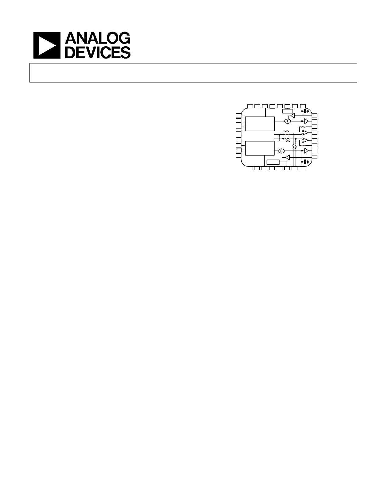
AD8364
FUNCTIONAL BLOCK DIAGRAM
DECA
COMA
Channel A
TruPwr™
Channel B
TruPwr™
DECB
COMB ADJB ADJA
OUTA
OUTB
o
C to +85oC.
VPSR ACMB TEMPACMA CLPA
TEMP
V2I
V2I
BIAS
VREF VLVL CLPB
87
16
VSTA
15
OUTA
14
FBKA
13
OUTP
OUTN
12
FBKB
11
10
OUTB
9
VSTB
CHPA
24 23 22 21 20 19 1718
25
VPSA
2
6
INHA
7
2
INLA
2
8
PWD
N
2
9
COMR
3
0
INLB
INHB
3
1
VPSB
3
2
1 2 3 4 5 6
CHPB
Figure 1. Functional Block Diagram
The device can easily be configured to provide three RMS
measurements simultaneously. Linear-in-dB RMS measurements are
supplied at OUTA and OUTB, with conveniently scaled slope of
50mV/dB. The RMS difference between OUTA and OUTB is
available differentially or single-ended at OUTP and OUTN. An
optional voltage applied to VLVL provides a common mode
reference level to offset OUTP and OUTN above ground.
Each channel of the AD8364 can independently be used to control
separate gain control feedback loops using VSTA and VSTB. The
difference outputs also provide feedback control while providing
improved temperature stability through matched channels.
Flexibility exists to use either channel as a reference while the other
channel is slaved through a feedback loop. RF power amplifier
control, VSWR measurements, and transceiver AGC circuits benefit
from this feature. In control modes, the opposite polarities of the
OUTP and OUTN outputs allow proportional or complementary
gain-control functions, eliminating the need for a board-level signinverting amplifier. Feedback pins FBKA and FBKB allow custom
loop regulation in special control system applications and log-slope
adjust flexibility. When one channel is slaved off the other,
controlling the voltage at VLVL will adjust the slaved channel’s RMS
value, if a power level offset is desired.
The AD8364 is supplied in a 32-lead 5x5mm LFCSP package, for the
operating temperature of –40
Rev. PrC 1/20/2005
Information furnished by Analog Devices is believed to be accurate and reliable.
However, no responsibility is assumed by Analog Devices for its use, nor for any
infringements of patents or other rights of third parties that may result from its use.
Specifications subject to change without notice. No license is granted by implication
or otherwise under any patent or patent rights of Anal og Devices. Trademarks and
registered trademarks are the property of their respective companies.
One Technology Way, P.O. Box 9106, Norwood, MA 02062-9106, U.S.A.
Tel: 781.329.4700 www.analog.com
Fax: 781.326.8703 © 2005 Analog Devices, Inc. All rights reserved.
Page 2

PRELIMINARY TECHNICAL DATA
(V
=VPSA=VPSB=VPSR =5V, T
AD8364-SPECIFICATIONS
Table I.
S
VST[A,B] = OUT[A,B], OUT[P,N] = FBK[A,B], differential input via Balun
input f ≤ 2.7GHz unless otherwise noted)
AD8364
=25°C, Chan A
A
= Chan B
FREQ
, VLVL = VREF,
FREQ
1
, CW
Parameters Conditions Min Typ Max Units
OVERALL FUNCTION
SIGNAL INPUT INTERFACE
Channel A and Channel B, CW sine wave input
INH[A,B] (Pins 26, 31) INL[A,B] (Pins 27, 30)
Specified Frequency Range LF 2.7 GHz
DC Common-Mode Voltage 2.5 V
SIGNAL OUTPUT INTERFACE
Small Signal Bandwidth
Slew Rate
Settling Time 10%-100% response of -45 dBm to 0 dBm modulated
100%-10% response of 0 dBm to -45 dBm modulated
Wideband Noise
MEASUREMENT MODE
450 MHz OPERATION
± 1 dB Dynamic Range
OUT[A,B] (Pins 15,10)
= C
C
LPA
C
LPA
pulse, C
pulse, C
CLPF = 1000pF, f
≤ 300pF
LPB
= C
≤ 300pF
LPB
=Open
LPA=CLPB
=Open,
LPA=CLPB
≤ 100KHz
SPOT
ADJA = ADJB = 0 V, Error Referred to Best Fit Line
using Linear Regression @ P
T
= 25oC, Balun = M/A-Com MABAES0054
A
-40dBm & -20dBm,
INH[A,B] =
Pins OUT[A,B]
TBD MHz
TBD
TBD
V/µS
µS
TBD nS
TBD
nV/√Hz
67 dB
-40oC < TA < +85oC 65 dB
±0.5 dB Dynamic Range -40oC < TA < +85oC 30 dB
Maximum Input Level ±1dB Error +15 dBm
Minimum Input Level ±1dB Error -52 dBm
Slope 50 mV/dB
Intercept -55 dBm
Output Voltage – High Power In
Output Voltage – Low Power In
Temperature Sensitivity
Pins OUT[A,B] @ P
Pins OUT[A,B] @ P
Deviation from OUT[A,B] @ 25°C
-40°C<TA<85°C; P
-40°C<TA<85°C; P
-40°C<TA<85°C; P
Deviation from OUT[P,N] @ 25°C
-40°C<TA<85°C; P
-40°C<T
-40°C<T
<85°C; P
A
<85°C; P
A
INH[A,B]
INH[A,B]
= -10dBm
= -40dBm
TBD 2.2 TBD
TBD 0.7 TBD
= -10dBm +/- 0.5 dB
INH[A,B]
= -25dBm +/- 0.5 dB
INH[A,B]
= -40dBm +/- 0.5 dB
INH[A,B]
= -10dBm, -10dBm +/- 0.3 dB
INH[A,B]
= -10dBm, -30dBm
INH[A,B]
= -10dBm, -40dBm
INH[A,B]
+/- 0.3
+/- 0.3
V
V
dB
dB
Deviation from CW Response 5.5dB Peak-to-RMS Ratio (WCDMA 1 Channel) TBD dB
12dB Peak-to-RMS Ratio (WCDMA 3 Channels) TBD dB
18dB Peak-to-RMS Ratio (WCDMA 4 Channels) TBD dB
Rev. PrC Ι Page 2 of 23
Page 3

PRELIMINARY TECHNICAL DATA AD8364
(V
=VPSA=VPSB=VPSR =5V, T
AD8364-SPECIFICATIONS
Table I.
S
VST[A,B] = OUT[A,B], OUT[P,N] = FBK[A,B], differential input via Balun
input f ≤ 2.7GHz unless otherwise noted)
Parameters Conditions Min Typ Max Units
InputA to InputB Isolation 30 dB
InputA to OUTB isolation
InputB to OUTA isolation (Note 1)
P
= -50dBm, OUTB = OUTB
INHB
P
= -50dBm, OUTA = OUTA
INHA
Input Impedance INHA/INLA, INHB/INLB Differential Drive
INHA/INLA, INHB/INLB Single-ended Drive
Input Return Loss With Recommended Balun TBD
MEASUREMENT MODE
ADJA = ADJB = 0 V, Error Referred to Best Fit Line
using Linear Regression @ P
880MHz OPERATION
± 1 dB Dynamic Range
= 25oC, Balun = M/A-Com ETC 1.6-4-2-3
T
A
Pins OUT[A,B]
-40oC < TA < +85oC 54 dB
±0.5 dB Dynamic Range -40oC < TA < +85oC 49 dB
Maximum Input Level ±1dB Error -2 dBm
Minimum Input Level ±1dB Error -61 dBm
Slope 50 mV/dB
Intercept -61 dBm
Output Voltage – High Power In
Output Voltage – Low Power In
Temperature Sensitivity
Pins OUT[A,B] @ P
Pins OUT[A,B] @ P
Deviation from OUT[A,B] @ 25°C
-40°C<TA<85°C; P
-40°C<TA<85°C; P
-40°C<TA<85°C; P
Deviation from OUT[P,N] @ 25°C
-40°C<TA<85°C; P
-40°C<T
-40°C<T
<85°C; P
A
<85°C; P
A
= -10dBm
INH[A,B]
= -40dBm
INH[A,B]
= -10dBm +/- 0.5 dB
INH[A,B]
= -25dBm +/- 0.5 dB
INH[A,B]
= -40dBm +/- 0.5 dB
INH[A,B]
= -25dBm, -10dBm +/- 0.3 dB
INH[A,B]
= -25dBm, -25dBm
INH[A,B]
= -25dBm, -40dBm
INH[A,B]
Deviation from CW Response 5.5dB Peak-to-RMS Ratio (WCDMA 1 Channel) 0.2 dB
12dB Peak-to-RMS Ratio (WCDMA 3 Channels) 0.3 dB
18dB Peak-to-RMS Ratio (WCDMA 4 Channels) 0.3 dB
InputA to InputB Isolation dB
InputA to OUTB isolation
InputB to OUTA isolation (Note 1)
= -50dBm, OUTB = OUTB
P
INHB
P
= -50dBm, OUTA = OUTA
INHA
Input Impedance INHA/INLA, INHB/INLB Differential Drive
INHA/INLA, INHB/INLB Single-ended Drive
Input Return Loss With Recommended Balun TBD
=25°C, Chan A
A
± 1 dB
PINHB
± 1 dB
PINHA
-40dBm & -20dBm,
INH[A,B] =
± 1 dB
PINHB
± 1 dB
PINHA
= Chan B
FREQ
, VLVL = VREF,
FREQ
TBD
210||0.1
TBD||TBD
59 dB
TBD 2.75 TBD
TBD 1.1 TBD
+/- 0.3
+/- 0.3
TBD
200||0.3
TBD||TBD
1
, CW
dB
Ω||pF
Ω||pF
V
V
dB
dB
dB
Ω||pF
Ω||pF
Rev. PrC Ι Page 3 of 23
Page 4

PRELIMINARY TECHNICAL DATA AD8364
(V
=VPSA=VPSB=VPSR =5V, T
AD8364-SPECIFICATIONS
Table I.
S
VST[A,B] = OUT[A,B], OUT[P,N] = FBK[A,B], differential input via Balun
input f ≤ 2.7GHz unless otherwise noted)
Parameters Conditions Min Typ Max Units
MEASUREMENT MODE
ADJA = ADJB = 0.75 V, Error Referred to Best Fit Line
using Linear Regression @ P
1880 MHz OPERATION
± 1 dB Dynamic Range
= 25oC, Balun = M/A-Com ETC 1.6-4-2-3
T
A
Pins OUT[A,B]
-40oC < TA < +85oC 52 dB
±0.5 dB Dynamic Range -40oC < TA < +85oC 49 dB
Maximum Input Level ±1dB Error -5 dBm
Minimum Input Level ±1dB Error -62 dBm
Slope 50 mV/dB
Intercept -62 dBm
Output Voltage – High Power In
Output Voltage – Low Power In
Temperature Sensitivity
Pins OUT[A,B] @ P
Pins OUT[A,B] @ P
Deviation from OUT[A,B] @ 25°C
-40°C<TA<85°C; P
-40°C<TA<85°C; P
-40°C<TA<85°C; P
Deviation from OUT[P,N] @ 25°C
-40°C<TA<85°C; P
-40°C<T
-40°C<T
<85°C; P
A
<85°C; P
A
= -10dBm
INH[A,B]
= -40dBm
INH[A,B]
= -10dBm +/- 0.5 dB
INH[A,B]
= -25dBm +/- 0.5 dB
INH[A,B]
= -40dBm +/- 0.5 dB
INH[A,B]
= -25dBm, -10dBm +/- 0.3 dB
INH[A,B]
= -25dBm, -25dBm
INH[A,B]
= -25dBm, -40dBm
INH[A,B]
Deviation from CW Response 5.5dB Peak-to-RMS Ratio (WCDMA 1 Channel) TBD dB
12dB Peak-to-RMS Ratio (WCDMA 3 Channels) TBD dB
18dB Peak-to-RMS Ratio (WCDMA 4 Channels) TBD dB
InputA to InputB Isolation dB
InputA to OUTB isolation
InputB to OUTA isolation (Note 1)
P
= -50dBm, OUTB = OUTB
INHB
P
= -50dBm, OUTA = OUTA
INHA
Input Impedance INHA/INLA, INHB/INLB Differential Drive
INHA/INLA, INHB/INLB Single-ended Drive
Input Return Loss With Recommended Balun TBD
MEASUREMENT MODE
ADJA = ADJB = 1.02 V, Error Referred to Best Fit Line
using Linear Regression @ P
2.14 GHz OPERATION
± 1 dB Dynamic Range
T
= 25oC, Balun = M/A-Com ETC 1.6-4-2-3
A
Pins OUT[A,B]
-40oC < TA < +85oC 51 dB
±0.5 dB Dynamic Range -40oC < TA < +85oC 45 dB
Maximum Input Level ±1dB Error -2 dBm
Minimum Input Level ±1dB Error -58 dBm
=25°C, Chan A
A
-40dBm & -20dBm,
INH[A,B] =
± 1 dB
PINHB
± 1 dB
PINHA
-40dBm & -20dBm,
INH[A,B] =
= Chan B
FREQ
, VLVL = VREF,
FREQ
57 dB
TBD 2.5 TBD
TBD 1.0 TBD
+/- 0.3
+/- 0.3
TBD
167||0.14
TBD||TBD
56 dB
1
, CW
V
V
dB
dB
dB
Ω||pF
Ω||pF
Rev. PrC Ι Page 4 of 23
Page 5

PRELIMINARY TECHNICAL DATA AD8364
(V
=VPSA=VPSB=VPSR =5V, T
AD8364-SPECIFICATIONS
Table I.
S
VST[A,B] = OUT[A,B], OUT[P,N] = FBK[A,B], differential input via Balun
input f ≤ 2.7GHz unless otherwise noted)
Parameters Conditions Min Typ Max Units
Slope 50 mV/dB
Intercept -58 dBm
Output Voltage – High Power In
Output Voltage – Low Power In
Temperature Sensitivity
Pins OUT[A,B] @ P
Pins OUT[A,B] @ P
Deviation from OUT[A,B] @ 25°C
-40°C<TA<85°C; P
-40°C<TA<85°C; P
-40°C<TA<85°C; P
Deviation from OUT[P,N] @ 25°C
-40°C<TA<85°C; P
-40°C<T
-40°C<T
<85°C; P
A
<85°C; P
A
= -10dBm
INH[A,B]
= -40dBm
INH[A,B]
= -10dBm +/- 0.5 dB
INH[A,B]
= -25dBm +/- 0.5 dB
INH[A,B]
= -40dBm +/- 0.5 dB
INH[A,B]
= -25dBm, -10dBm +/- 0.3 dB
INH[A,B]
= -25dBm, -25dBm
INH[A,B]
= -25dBm, -40dBm
INH[A,B]
Deviation from CW Response 5.5dB Peak-to-RMS Ratio (WCDMA 1 Channel) 0.2 dB
12dB Peak-to-RMS Ratio (WCDMA 3 Channels) 0.3 dB
18dB Peak-to-RMS Ratio (WCDMA 4 Channels) 0.3 dB
InputA to InputB Isolation dB
InputA to OUTB isolation
InputB to OUTA isolation (Note 1)
P
= -50dBm, OUTB = OUTB
INHB
P
= -50dBm, OUTA = OUTA
INHA
Input Impedance INHA/INLA, INHB/INLB Differential Drive
INHA/INLA, INHB/INLB Single-ended Drive
Input Return Loss With Recommended Balun TBD
MEASUREMENT MODE
ADJA = ADJB = 1.14 V, Error Referred to Best Fit Line
using Linear Regression @ P
2.5 GHz OPERATION
± 1 dB Dynamic Range
T
= 25oC, Balun = M/A-Com ETC 1.6-4-2-3
A
Pins OUT[A,B]
-40oC < TA < +85oC 52 dB
±0.5 dB Dynamic Range -40oC < TA < +85oC 42 dB
Maximum Input Level ±1dB Error 5 dBm
Minimum Input Level ±1dB Error -53 dBm
Slope 50 mV/dB
Intercept -53 dBm
Output Voltage – High Power In
Output Voltage – Low Power In
Pins OUT[A,B] @ P
Pins OUT[A,B] @ P
INH[A,B]
INH[A,B]
= -10dBm
= -40dBm
=25°C, Chan A
A
± 1 dB
PINHB
± 1 dB
PINHA
-40dBm & -20dBm,
INH[A,B] =
= Chan B
FREQ
, VLVL = VREF,
FREQ
TBD 2.3 TBD
TBD 0.85 TBD
+/- 0.3
+/- 0.3
TBD
150||1.9
TBD||TBD
58 dB
TBD 2.1 TBD
TBD 0.65 TBD
1
, CW
V
V
dB
dB
dB
Ω||pF
Ω||pF
V
V
Rev. PrC Ι Page 5 of 23
Page 6

PRELIMINARY TECHNICAL DATA AD8364
(V
=VPSA=VPSB=VPSR =5V, T
AD8364-SPECIFICATIONS
Table I.
S
VST[A,B] = OUT[A,B], OUT[P,N] = FBK[A,B], differential input via Balun
input f ≤ 2.7GHz unless otherwise noted)
Parameters Conditions Min Typ Max Units
Temperature Sensitivity
-40°C<TA<85°C; P
-40°C<TA<85°C; P
-40°C<TA<85°C; P
-40°C<TA<85°C; P
Deviation from OUT[A,B] @ 25°C
= -10dBm +/- 0.5 dB
INH[A,B]
= -25dBm +/- 0.5 dB
INH[A,B]
= -40dBm +/- 0.5 dB
INH[A,B]
Deviation from OUT[P,N] @ 25°C
= -25dBm, -10dBm +/- 0.3 dB
INH[A,B]
-40°C<T
-40°C<T
<85°C; P
A
<85°C; P
A
= -25dBm, -25dBm
INH[A,B]
= -25dBm, -40dBm
INH[A,B]
Deviation from CW Response 5.5dB Peak-to-RMS Ratio (WCDMA 1 Channel) TBD dB
12dB Peak-to-RMS Ratio (WCDMA 3 Channels) TBD dB
18dB Peak-to-RMS Ratio (WCDMA 4 Channels) TBD dB
InputA to InputB Isolation dB
InputA to OUTB isolation
InputB to OUTA isolation (Note 1)
P
= -50dBm, OUTB = OUTB
INHB
P
= -50dBm, OUTA = OUTA
INHA
Input Impedance INHA/INLA, INHB/INLB Differential Drive
INHA/INLA, INHB/INLB Single-ended Drive
Input Return Loss With Recommended Balun TBD
MEASUREMENT MODE
ADJA = ADJB = 1.18 V, Error Referred to Best Fit Line
using Linear Regression @ P
2.7 GHz OPERATION
± 1 dB Dynamic Range
T
= 25oC, Balun = M/A-Com ETC 1.6-4-2-3
A
Pins OUT[A,B]
-40oC < TA < +85oC 55 dB
±0.5 dB Dynamic Range -40oC < TA < +85oC 45 dB
Maximum Input Level ±1dB Error 10 dBm
Minimum Input Level ±1dB Error -50 dBm
Slope 49 mV/dB
Intercept -51 dBm
Output Voltage – High Power In
Output Voltage – Low Power In
Temperature Sensitivity
-40°C<TA<85°C; P
-40°C<TA<85°C; P
-40°C<TA<85°C; P
Pins OUT[A,B] @ P
Pins OUT[A,B] @ P
INH[A,B]
INH[A,B]
= -10dBm
= -40dBm
Deviation from OUT[A,B] @ 25°C
= -10dBm +/- 0.5 dB
INH[A,B]
= -25dBm +/- 0.5 dB
INH[A,B]
= -40dBm +/- 0.5 dB
INH[A,B]
=25°C, Chan A
A
± 1 dB
PINHB
± 1 dB
PINHA
-40dBm & -20dBm,
INH[A,B] =
= Chan B
FREQ
, VLVL = VREF,
FREQ
+/- 0.3
+/- 0.3
TBD
150||1.7
TBD||TBD
60 dB
TBD 2.0 TBD
TBD 0.5 TBD
1
, CW
dB
dB
dB
Ω||pF
Ω||pF
V
V
Rev. PrC Ι Page 6 of 23
Page 7

PRELIMINARY TECHNICAL DATA AD8364
(V
=VPSA=VPSB=VPSR =5V, T
AD8364-SPECIFICATIONS
Table I.
S
VST[A,B] = OUT[A,B], OUT[P,N] = FBK[A,B], differential input via Balun
input f ≤ 2.7GHz unless otherwise noted)
Parameters Conditions Min Typ Max Units
-40°C<TA<85°C; P
Deviation from OUT[P,N] @ 25°C
= -25dBm, -10dBm +/- 0.3 dB
INH[A,B]
-40°C<T
-40°C<T
<85°C; P
A
<85°C; P
A
= -25dBm, -25dBm
INH[A,B]
= -25dBm, -40dBm
INH[A,B]
Deviation from CW Response 5.5dB Peak-to-RMS Ratio (WCDMA 1 Channel) TBD dB
12dB Peak-to-RMS Ratio (WCDMA 3 Channels) TBD dB
18dB Peak-to-RMS Ratio (WCDMA 4 Channels) TBD dB
InputA to InputB Isolation TBD dB
InputA to OUTB isolation
InputB to OUTA isolation (Note 1)
P
= -50dBm, OUTB = OUTB
INHB
P
= -50dBm, OUTA = OUTA
INHA
Input Impedance INHA/INLA, INHB/INLB Differential Drive
INHA/INLA, INHB/INLB Single-ended Drive
Input Return Loss With Recommended Balun TBD
OUTPUT INTERFACE
Voltage Range Min
Voltage Range Max
Source/Sink Current
SET-POINT INPUT
Voltage Range
Pin OUTA and OUTB
≥ 200Ω to ground
R
L
≥ 200Ω to ground
R
L
OUTA & OUTB held at V
/2, to 1% change
S
Pin VSTA and VSTB
Law conformance error ≤ ±1dB
Input Resistance 68
Logarithmic Scale Factor
Logarithmic Intercept
f = 450MHz??, -40°C ≤ T
f = 450MHz??, -40°C ≤ T
≤ +85°C
A
≤ +85°C, Re: 50Ω
A
Temperature Sensitivity Pin = -10dBm, slope and intercept errors combined TBD
DIFFERENCE OUTPUT
Voltage Range Min
Voltage Range Max
Source/Sink Current
Small Signal Bandwidth
Slew Rate
Wideband Noise
Offset
Pin OUTP and OUTN
≥ 200Ω to ground
R
L
≥ 200Ω to ground
R
L
OUTP and OUTN held at V
≤ 300pF
C
L
≤ 300pF
C
L
CLPF = 1000pF, f
SPOT
/2, to 1% change
S
≤ 100KHz
OUTB=OUTA=open, OUTP=FBKA=open,
VLVL=open
=25°C, Chan A
A
± 1 dB
PINHB
± 1 dB
PINHA
= Chan B
FREQ
+/- 0.3
+/- 0.3
, VLVL = VREF,
FREQ
1
, CW
dB
dB
dB
TBD
200||0.08
TBD||TBD
Ω||pF
Ω||pF
0.09
VS-0.05
V
V
70 mA
0.5 3.75 V
KΩ
50 mV/dB
-55 dBm
dB/°C
0.1
VS-0.15
V
V
70 mA
TBD MHz
TBD
TBD
V/µS
nV/√Hz
TBD mV
DIFFERENCE LEVEL ADJUST
Voltage Range
Pin VLVL
OUT[P,N]=FBK[A,B} (through Cap)
OUT[P,N] Voltage Range OUT[P,N]=FBK[A,B} (through Cap)
0 TBD V
0 TBD V
Input Resistance 1
Rev. PrC Ι Page 7 of 23
KΩ
Page 8

PRELIMINARY TECHNICAL DATA AD8364
(V
=VPSA=VPSB=VPSR =5V, T
AD8364-SPECIFICATIONS
Table I.
S
VST[A,B] = OUT[A,B], OUT[P,N] = FBK[A,B], differential input via Balun
input f ≤ 2.7GHz unless otherwise noted)
Parameters Conditions Min Typ Max Units
TEMPERATURE COMPENSATION
Pin ADJA and ADJB
Input Voltage Range 0 2.5 V
Input Resistance <1
VOLTAGE REFERENCE
Pin VREF
Output Voltage RF in = -55 dBm 2.5 V
Temperature Sensitivity
-40°C ≤ T
≤ +85°C
A
Current Limit Source/Sink Into a grounded load /to 1% change 18/6 mA
TEMPERATURE REFERENCE
Output Voltage
Temperature Slope
Current Source/Sink
POWER DOWN INTERFACE
Pin TEMP
=25°C, RL=10KΩ
T
A
-40°C ≤ T
T
A
≤ +85°C, RL=10KΩ
A
=25°C to 1% change
Pin PWDN
Logic Level to Enable Logic LO enables 1 V
Logic Level to Disable Logic HI disables 3 V
Input Current
Logic HI PWDN = 5V
Logic LO PWDN = 0V
Enable Time PWDN LO to OUTA/OUTB at 100% final value,
C
=Open, C
LPA/B
=10nF RF in = 0 dBm
HPA/B
Disable Time PWDN HI to OUTA/OUTB at 10% final value,
C
POWER INTERFACE
=Open, C
LPA/B
Pin VPS[A,B], VPSR
=10nF, RF in = 0 dBm
HPA/B
Supply Voltage 4.5 5.5 V
Quiescent Current RF in = -55 dBm, Vs =5V 72 TBD mA
Supply Current
Notes (not complete)
PWDN enabled, Vs =5V
1. See Figure/TPC X for a plot of isolation versus frequency for a ± 1 dB error
2. See Figure/TPC X
3. Best Fit Line, Linear Regression
=25°C, Chan A
A
= Chan B
FREQ
, VLVL = VREF,
FREQ
0.22
0.6 V
2
1.6/2 mA
100
<1
2
1.6
500
1
, CW
MΩ
mV/°C
mV/°C
µA
µA
µS
µS
µA
Rev. PrC Ι Page 8 of 23
Page 9

PRELIMINARY TECHNICAL DATA AD8364
ABSOLUTE MAXIMUM RATINGS
Table 2. ADL5306 Absolute Maximum Ratings
Parameter Rating
Supply Voltage VPSA, VPSB, VPSR
PWDN, VSTA, VSTB, ADJA, ADJB
Input power (Re: 50Ω)
Internal Power Dissipation
θ
JA
Maximum Junction Temperature
Operating Temperature Range
Storage Temperature Range
Lead Temperature Range (Soldering 60 sec
5.5V
0V, 5.5V
TBD dBm
TBDmW
TBD C/W
+125° C.
-40° C to +85° C
-65° C to +150° C
+300° C
Stresses above those listed under Absolute Maximum Ratings
may cause permanent damage to the device. This is a stress
rating only; functional operation of the device at these or any
other conditions above those indicated in the operational
section of this specification is not implied. Exposure to absolute
maximum rating conditions for extended periods may affect
device reliability.
Rev. PrC Ι Page 9 of 23
Page 10

PRELIMINARY TECHNICAL DATA
AD8364
PIN CONFIGURATION AND FUNCTIONAL DESCRIPTIONS
CHPA
24
25
VPSA
2
6
INHA
7
INLA
2
2
8
PWD
N
COMR
2
9
3
0
INLB
INHB
3
1
VPSB
3
2
1
CHPB
Table 3. Pin Function Descriptions
Pin Name Description Equiv.
1
2,23
3, 22, 29
4, 5
6
7
8, 17
9
10
11
12
13
14
15
16
18, 20
21,25,32
19
24
26, 27
28
30, 31
Under
Package
CHPB
DECA, DECB
COMB, COMA
COMR
ADJB, ADJA
VREF
VLVL
CLPB, CLPA
VSTB
OUTB
FBKB
OUTN
OUTP
FBKA
OUTA
VSTA
ACMA, ACMB
VPSR, VPSA
VPSB
TEMP
CHPA
INHA, INLA
PWDN
INLB, INHB
Exposed
Paddle
Connect to common via a capacitor to determine 3 dB point of Channel B input signal high-pass filter.
Decoupling terminals for INHA/INLA and INHB/INLB. Connect to common via a large
capacitance to complete input circuit.
Input system common connection. Connect via low impedance to system common.
Temperature compensation for Channel B and Channel A. An external voltage is connected to these
pins to improve temperature drift. This voltage can be derived from Vref, that is, connect a resistor
from Vref to ADJ[A,B] and another resistor from ADJ[A,B] to ground. The value of these resistors will
change with frequency.
General-purpose reference voltage output of 2.5V.
Reference level input for OUTP and OUTN. (Usually connected to VREF through a voltage divider or
left open).
Channel B and Channel A connection for loop filter integration (averaging) capacitor. Connect a
ground-referenced capacitor to this pin. A resistor can be connected in series with this capacitor to
improve loop stability and response time.
The voltage applied to this pin sets the decibel value of the required RF input voltage to Channel B that
results in zero current out of the loop integrating capacitor pin, CLPB.
Channel B output of error amplifier. In measurement mode, normally connected directly to VSTB.
Feedback through 1KΩ to the negative terminal of the integrated op-amp driving OUTN.
Output of differencing op-amp. In measurement mode, normally connected directly to FBKB.
Output of differencing op-amp. In measurement mode, normally connected directly to FBKA.
Feedback through 1KΩ to the negative terminal of the integrated op-amp driving OUTP.
Channel A output of error amplifier. In measurement mode, normally connected directly to VSTA.
The voltage applied to this pin sets the decibel value of the required RF input voltage to Channel A
that results in zero current out of the loop integrating capacitor pin, CLPA.
Analog common for channel A &B. Connect via low impedance to common.
Supply for the input system of channel A & B. Supply for the internal references. Connect to +5 V
power supply.
Temperature sensor output.
Connect to common via a capacitor to determine 3 dB point of Channel A input signal high-pass filter.
Channel A “High” and “Low” RF signal input terminal. Circuit A
Disable/Enable control input. Apply logic high voltage to shut AD8364 down.
Channel B “Low” and “High” RF signal input terminal. Circuit A
The exposed paddle on the under side of the package should be soldered to a low thermal and
electrical impedance ground plane.
VPSR ACMB TEMP ACMA CLPA
DECA
COMA
23
22
21
20
19
TEMP
Channel A
TruPwr™
OUTA
OUTB
Channel B
TruPwr™
V2I
BIAS
2
3
4
5
6
DECB
COMB ADJB ADJA
VREF VLVL CLPB
Figure 2. AD8364 Pinout
17
18
16
V2I
7
VSTA
15
OUTA
14
FBKA
13
OUTP
OUTN
12
FBKB
11
10
OUTB
9
VSTB
8
Circuit
Rev. PrC Ι Page 10 of 23
Page 11

PRELIMINARY TECHNICAL DATA AD8364
TYPICAL PERFORMANCE CHARACTERISTICS
V
= 5 V, T = +25°C, –40°C, +85°C; C
P
= OPEN. Colors: +25°C Black; –40°C Blue; +85°C Red
LPA/B
5
4.5
4
3.5
3
2.5
OUTA (V)
2
1.5
1
0.5
0
-60 -55 -50 -45 -40 -35 -30 -25 -20 -15 -10 -5 0 5 10 15 20
Figure 3.OUT[A,B] V
5
4.5
4
3.5
3
2.5
OUTA (V)
2
1.5
1
0.5
0
-65 -60 -55 -50 -45 -40 -35 -30 -25 -20 -15 -10 -5 0 5 10
Figure 4. OUT[A,B] V
Typical D evice, T
5
4.5
4
3.5
3
2.5
OUTA (V)
2
1.5
1
0.5
0
-65 -60 -55 -50 -45 -40 -35 -30 -25 -20 -15 -10 -5 0 5 10
Figure 5. OUT[A,B] V
Typical D evice, T
Pin (dBm)
and Log Conformance vs. Input Amplitude at 450 MHz, Typical
OUT
Device, T
= 0V, Sine Wave, Differential Drive
ADJA/B
Pin (dBm)
and Log Conformance vs. Input Amplitude at 880 MHz,
OUT
OUT
= 0V, Sine Wave, Differential Drive
ADJA/B
Pin (dBm)
and Log Conformance vs. Input Amplitude at 1.88 GHz,
= 0.75V , Sine Wave, Differential Drive
ADJA/B
5
2.5
2
1.5
1
0.5
)
A (dB
0
ERROR
-0.5
-1
-1.5
-2
-2.5
2.5
2
1.5
1
0.5
0
ERROR A (dB)
-0.5
-1
-1.5
-2
-2.5
2.5
2
1.5
1
0.5
0
ERROR A (dB)
-0.5
-1
-1.5
-2
-2.5
4.5
4
3.5
3
2.5
OUTA (V)
2
1.5
1
0.5
0
-65 -60 -55 -50 -45 -40 -35 -30 -25 -20 -15 -10 -5 0 5 10
Figure 6. OUT[A,B] V
Typical D evice, T
5
4.5
4
3.5
3
2.5
OUTA (V)
2
1.5
1
0.5
0
-65 -60 -55 -50 -45 -40 -35 -30 -25 -20 -15 -10 -5 0 5 10
Figure 7. OUT[A,B] V
Device, T
Pin (dBm)
and Log Conformance vs. Input Amplitude at 2.14 GHz,
OUT
and Log Conformance vs. Input Amplitude at 2.5 GHz, Typical
OUT
=1.02V , Sine Wave, Differential Drive
ADJA/B
Pin (dBm)
=1.14V , Sine Wave, Differential Drive
ADJA/B
100 MHz
2700 MHz
Figure 8. Differential Input Impedance (S11) vs. Frequency; Zo = 50
2.5
2
1.5
1
0.5
0
ERROR A (dB)
-0.5
-1
-1.5
-2
-2.5
2.5
2
1.5
1
0.5
0
ERROR A (dB)
-0.5
-1
-1.5
-2
-2.5
Ω
Rev. PrC Ι Page 11 of 23
Page 12

PRELIMINARY TECHNICAL DATA AD8364
5
4.5
4
3.5
3
2.5
OUT[P,N] (V)
2
1.5
1
0.5
0
-65 -60 -55 -50 -45 -40 -35 -30 -25 -20 -15 -10 -5 0 5 10
Figure 9. OUT[P,N] V
and Log Conformance vs. Input Amplitude at 450 MHz, With B
OUT
Pin (dBm)
input held at -25dBM and A input swept, Typical Device, T
Differential Drive
5
4.5
4
3.5
3
2.5
OUT[P,N] (V)
2
1.5
1
0.5
0
-65 -60 -55 -50 -45 -40 -35 -30 -25 -20 -15 -10 -5 0 5 10
Figure 10. OUT[P,N] V
and Log Conformance vs. Input Amplitude at 880 MHz, With
OUT
Pin (dBm)
B input held at -25dBM and A input swept, Typical Device, T
Differential Drive
5
4.5
4
3.5
3
2.5
OUT[P,N] (V)
2
1.5
1
0.5
0
-65 -60 -55 -50 -45 -40 -35 -30 -25 -20 -15 -10 -5 0 5 10
Figure 11. OUT[P,N] V
and Log Conformance vs. Input Amplitude at 1.88 GHz, With
OUT
Pin (dBm)
B input held at -25dBM and A input swept, Typical Device, T
Differential Drive
=0V, Sine Wave,
ADJA/B
=0V, Sine Wave,
ADJA/B
=0.75V, Sine Wave,
ADJA/B
5
4
3
2
1
0
ERROR [P,N] (dB)
-1
-2
-3
-4
-5
5
4.5
4
3.5
3
2.5
OUT[P,N] (V)
2
1.5
1
0.5
0
-65 -60 -55 -50 -45 -40 -35 -30 -25 -20 -15 -10 -5 0 5 10
Figure 12. OUT[P,N] V
Pin (dBm)
and Log Conformance vs. Input Amplitude at 2.14 GHz, With
OUT
B input held at -25dBM and A input swept, Typical Device, T
Differential Drive
5
4
3
2
1
0
ERROR [P,N] (dB)
-1
-2
-3
-4
-5
5
4.5
4
3.5
3
2.5
OUT[P,N] (V)
2
1.5
1
0.5
0
-65 -60 -55 -50 -45 -40 -35 -30 -25 -20 -15 -10 -5 0 5 10
Figure 13. OUT[P,N] V
Pin (dBm)
and Log Conformance vs. Input Amplitude at 2.5 GHz, With B
OUT
input held at -25dBM and A input swept, Typical Device, T
Differential Drive
5
4
3
2
1
0
ERROR [P,N] (dB)
-1
-2
-3
-4
-5
2
1.5
1
0.5
0
ERROR (dB)
-0.5
-1
-1.5
-2
-65-60-55-50-45-40-35-30-25-20-15-10 -5 0 5 10
Pin (dBm)
Figure 14. Distribution of OUT[A,B] Error over Temperature after Ambient
Normalization vs. Input Amplitude for 10 Devices, Frequency=450 MHz, T
Sine Wave, Differential Drive
=1.02V, Sine Wave,
ADJA/B
=1.14V, Sine Wave,
ADJA/B
ADJA/B
5
4
3
2
1
0
-1
-2
-3
-4
-5
5
4
3
2
1
0
-1
-2
-3
-4
-5
ERROR [P,N] (dB)
ERROR [P,N] (dB)
= 0V,
Rev. PrC Ι Page 12 of 23
Page 13

PRELIMINARY TECHNICAL DATA AD8364
2
2
1.5
1
0.5
0
ERROR (dB)
-0.5
-1
-1.5
-2
-65 -60 -55 -50 -45 -40 -35 -30 -25 -20 -15 -10 -5 0 5 10
Pin (dBm)
Figure 15. Distribution of OUT[A,B] Error at Temperature after Ambient Normalization
vs. Input Amplitude for 10 Devices, Frequency= 880 MHz, T
= 0V , Sine Wave,
ADJA/B
Differential Drive
2
1.5
1
0.5
0
ERROR (dB)
-0.5
-1
-1.5
-2
-65 -60 -55 -50 -45 -40 -35 -30 -25 -20 -15 -10 -5 0 5 10
Pin (dBm)
Figure 16. Distribution of OUT[A,B] Error at Temperature after Ambient Normalization
vs. Input Amplitude for 10 Devices, Frequency=1.88 GHz, T
= 0.75V, Sine Wave,
ADJA/B
Differential Drive
2
1.5
1
0.5
0
ERROR (dB)
-0.5
-1
-1.5
-2
-65-60-55-50-45-40-35-30-25-20-15-10 -5 0 5 10
Pin (dBm)
Figure 18. Distribution of OUT[A,B] Error at Temperature after Ambient Normalization
vs. Input Amplitude for 10 Devices, Frequency=2.5 GHz, T
= 1.14V , Sine Wave,
ADJA/B
Differential Drive
2
1
Phase: INLx wrt INHx
0
Error (d B)
-1
Ideal
+5°
-5°
+15°
-15°
-1dB
INHx < INLx
-2
-40 -30 -20 -10 0 10 20
RFin (dBm)
Figure 19. V
and Log Conformance vs. Input Amplitude for magnitude balance of 0
OUT
dB, and -1 dB and phase balance of 0 deg, ±5 deg, ±15 deg at 450 MHz, Typical Device,
T
= 0V, Sine Wave, Differential Drive
ADJA/B
1.5
1
0.5
0
ERROR (dB)
-0.5
-1
-1.5
-2
-65 -60 -55 -50 -45 -40 -35 -30 -25 -20 -15 -10 -5 0 5 10
Pin (dBm)
Figure 17. Distribution of OUT[A,B] Error at Temperature after Ambient Normalization
vs. Input Amplitude for 10 Devices, Frequency=2.14 GHz, T
= 1.02V , Sine Wave,
ADJA/B
Differential Drive
Rev. PrC Ι Page 13 of 23
Figure 20. Output Response to RF Burst Input for Various
RF Input Levels, Carrier Frequency 450 MHz, CLPA/B = 0
Page 14

PRELIMINARY TECHNICAL DATA AD8364
Figure 21. Output Response to RF Burst Input for Various RF Input Levels, Carrier
Frequency 450 MHz, CLPA/B = 0.1 µF
14
TOTAL = 40 DEVICES
12
10
8
Count
6
4
2
0
2.486 2.488 2.49 2.492 2.494 2.496 2.498 2.5 2.502 2.504 2.506
VREF (VOLTS)
RF INPUT = -60 dBm
Figure 24. Distribution of VREF for 40 Devices
8
7
TOTAL = 40 DEVICES
RF INPUT = -60 dBm
6
5
Figure 22. Output Response Using Power-Down Mode for Various RF Input Levels,
Carrier Frequency 450 MHz, CLPA = 0
Figure 23. Output Response Using Power-Down Mode for Various RF Input Levels,
Carrier Frequency 450 MHz, CLPA = 0.1 µF, CHPA = 10nF
4
Count
3
2
1
0
0.617 0.619 0.621 0.623 0.625 0.627
TEMP (VOLTS)
Figure 25. Distribution of TEMP voltage for 40 Devices
20
15
10
5
0
Change in VREF (mV)
-5
-10
-15
-20
-40-30-20-100 102030405060708090
Temp (degC)
Figure 26. Change in VREF vs. Temperature, 11 parts
Rev. PrC Ι Page 14 of 23
Page 15

PRELIMINARY TECHNICAL DATA AD8364
4
3.5
3
2.5
2
OUTA (Volts)
1.5
1
0.5
0
-60 -55 -50 -45 -40 -35 -30 -25 -20 -15 -10 -5 0 5 10
Figure 27.
Output Voltage and Error from CW Linear Reference vs. Input
Pin (dBm)
2
1.5
1
0.5
0
-0.5
-1
-1.5
-2
Amplitude with Different Waveforms, CW, WCDMA1,3,4 and 11Channel, Frequency 880MHz.
4
3.5
3
2.5
2
OUTA (Volts)
1.5
1
0.5
0
-60 -55 -50 -45 -40 -35 -30 -25 -20 -15 -10 -5 0 5 10
2
1.5
1
0.5
0
-0.5
-1
-1.5
-2
Pin (dBm)
Figure 28. Output Voltage and Error from CW Linear Reference vs. Input
Amplitude with Different Waveforms, CW, WCDMA 1,3,4-Channel,
Frequency 2140 MHz
CW VOUT
1 CHANNEL
VOUT
3 CHANNEL
VOUT
4 CHANNEL
VOUT
11 CHANNEL
VOUT
ERROR (dB)
CW ERROR
1 CHANNEL
ERROR
3 CHANNEL
ERROR
4 CHANNEL
ERROR
11 CHANNEL
ERROR
CW VOUT
1 CHANNEL
VOUT
3 CHANNEL
VOUT
4 CHANNEL
VOUT
ERROR (dB)
CW ERROR
1 CHANNEL
ERROR
3 CHANNEL
ERROR
4 CHANNEL
ERROR
Rev. PrC Ι Page 15 of 23
Page 16

PRELIMINARY TECHNICAL DATA AD8364
U
T
V
V
N
V
V
F
A
A
T
A
F
GENERAL DESCRIPTION AND THEORY
Square Law Detector and Amplitude Target
The AD8364 is a dual channel 2.7GHz true RMS responding
detector with 60 dB measurement range and incorporates two
AD8362 channels with shared reference circuitry (See the
AD8362 datasheet for more information). Multiple enhancements
have been made to the AD8362 cores to improve measurement
accuracy. Log-conformance peak-to-peak ripple has been
reduced to < ±0.2 dB, over the entire dynamic range.
Temperature stability of the RMS output measurements provides
o
< ± 0.5 dB error over the specified temperature range of -40
o
85
C, through proprietary techniques. The use of well matched
C to
channels offers extremely temperature stable channel difference
outputs at OUTP and OUTN. Given well matched channels
through IC integration, the RMS measurement outputs, OUTA
and OUTB, will drift in the same manner (<± 0.5 dB). With
OUTP shorted to FBKA, the func tion at OUTP is:
OUTP = OUTA – OUTB + VLVL (1)
When OUTN is shorted to FBKB, the function at OUTN is:
OUTN = OUTB – OUTA + VLVL (2)
The difference outputs, OUTP and OUTN, are insensitive to the
common drift due to the difference cancellation of OUTA and
OUTB.
The AD8364 is a fully calibrated RMS-to-DC converter capable
of operation from signals as low as a few Hertz to at least 2.7GHz.
Unlike logarithmic amplifiers, the AD8364 response is waveform
independent. The device accurately measures waveforms having
a high peak-to-rms ratio (crest factor). A block diagram is shown
below in figure 29.
VPSA
INHA
INLA
PWDN
COMR
INLB
INHB
VPSB
CHPA
24 23 22
25
6
2
2
2
2
3
3
3
Channel A
TruPwr™
7
8
9
0
Channel B
TruPwr™
1
2
1 2 3 4 5 6
CHPB COMB
DECB
VPSR ACOM TEMPACOM CLPA
COMA
DECA
OUTA
OUTB
ADJB
21
BIAS
20
19
TEMP
V2I
VREF VLVL CLPB
ADJA
Figure 29. Block Diagram
1718
16
V2I
87
VSTA
15
OUTA
14
FBKA
13
OUTP
OUTN
22
FBKB
11
10
OUTB
9
VSTB
A single channel of the AD8364 consists of a high performance
AGC loop. Referring to figure 30, the AGC loop is comprised of
a wide bandwidth variable gain amplifier (VGA), square law
detectors, Amplitude Target circuit, and output driver.
For more
detailed description of the functional blocks, see AD8362 data sheet.
The output of the VGA, called V
, is applie d to a wideband
SIG
square law detector. The detector provides the true RMS
response of the RF input signal, independent of waveform,
up to crest factors of 6. The detector output, called I
SQU
, is a
fluctuating current with positive mean value. The difference
between I
integrated by C
and an internally generated current, I
SQU
and a capacitor attached to CLP[A,B]. C
F
TGT[A,B]
,is
F
is the on chip 25pF filter capacitor. CLP[A,B] can be used
to arbitrarily increase the averaging time while trading off
response time. When the AGC loop is at equilibrium:
MEAN(I
SQU
) = I
TGT[A,B]
(3)
This equilibrium occurs only when:
MEAN(V
Where V
is an attenuated version of the V
TGT
SIG
2
) = V
TGT[A,B]
2
(4)
voltage.
REF
Since the square law detectors are electrically identical and
well matched, process and temperature-dependant variations
are effectively cancelled.
INH[A,B]
INL[A,B]
CHP[A,B]
ST[A,B]
REF
-28 to +40dB
V
Offset –
Nulling
ST[A,B]
V
RE
2.5V
I
VGA
Set-Point
Interface
Band-Gap
Reference
G
SE
x
SIG
I
CLP[A,B]
C
external
Figure 30. Single Channel Details
Matched Wide
Band Squarers
2
SQ
LPF
2
x
I
TG
C
mplitudeTarget
for V
SIG
Temperature
Compensation
V
RE
Output
F
Buffer
Internal resistors
set buffer gain to 5
V
OUT[A,B]
DJ[A,B]
OUT[A,B]
COM
By forcing the above identity through varying the VGA setpoint, it is apparent that:
RMS(V
) = √(MEAN(V
SIG
Substituting the value of V
RMS(G
*RFIN exp(-V
0
2
)) = √(V
SIG
, we have:
SIG
ST[A,B]/VGNS
TGT
)) = V
2
) = V
TGT
TGT
(5)
(6)
When connected as a measurement device VST[A,B] =
OUT[A,B]. Solv ing for OUT[A,B] as a function of RF
OUT[A,B] = V
*Log10(RMS(RFIN)/VZ)
SLOPE
:
IN
(7)
Where V
the intercept voltage, since Log10(1) = 0 when RMS(RF
V
. If desired, the effective value of V
Z
is approximately1V/decade or 50mV/dB. VZ is
SLOPE
may be altered by
SLOPE
) =
IN
Rev. PrC Ι Page 16 of 23
Page 17

PRELIMINARY TECHNICAL DATA AD8364
V
V
V
using a resistor divider from OUT[A,B] to drive VST[A,B].
The intercept, V
, is approximately 316µV (-70 dBV) with a CW
Z
signal. This is the extrapolated intercept since OUT[A,B] does
not measure down to 0V.
In most applications, the AGC loop is closed through the set
point interface, VST[A,B]. In measurement mode, OUT[A,B]
is tied to VST[A,B], respectively. In controller mode, a control
voltage is applied to VST[A,B]. Pins OUT[A,B] drive the
control input of a system. The RF feedback signal to the input
pins is forced to have an RMS value determined by VSTA or
VSTB.
RF Input interface
The AD8364’s RF inputs are connected as shown in figure 31.
There are 100Ω resistors connected between DEC[A,B] and
INH[A,B] and INL[A,B]. The mid-point is wired to a pin called
DEC[A,B]. Internally to the IC, the DC level on DEC[A,B] is
established as (7*VPS[A,B] + 55*Vbe)/30. With a 5V supply,
DEC[A,B] is at about 2.6V.
Signal coupling capacitors must be connected from the input
signal to the INH[A,B] and INL[A,B] pins. The high-pass corner
is found as:
= 1/(2*π*100*C) (8)
f
high-pass
A decoupling capacitor should be connected from DEC[A,B] to
ground to attenuate any signal at the mid-point. A 100pF and
0.1 F cap from DEC[A,B] to ground are recommended with a
1nF coupling capacitor such that signals above 1.6MHz can be
measured. For coupling of signals below 1.6MHz, a good rule of
thumb would be to use 100*C
DEC[A,B]
for the DEC[A,B] capacitor.
coupling
POS
COMM
INH[A,B]
V
INL[A,B]
POS
IN
POS
VGA
(1/(2*π*5KΩ*25pF)), sufficiently low for most HF
applications. The high pass corner can be reduced by a
capacitor from CHP[A,B] to ground. The input offset
voltage varies depending on the actual gain at which the
VGA is operating, and thus, on the input signal amplitude.
When an excessively large value of C
is used, the offset
HP[A,B]
correction process may lag the more rapid changes in the
VGA’s gain, which may increase the time required for the
loop to fully settle for a given steady input amplitude.
Temperature Sensor Interface
The AD8364 provides a temperature sensor output capable
of driving about 1.6 mA. A 330Ω internal resistor is
connected from TEMP to COMR to provide current sink
capability. The temperature scaling factor of the output
voltage is approximately 2mV/
o
voltage at 27
C is about 630 mV.
o
C. The typical absolute
VREF Interface
An internal voltage reference is provided to the user at pin
VREF. The VREF voltage is a temperature stable 2.5V
reference that can drive about 18mA. An 830Ω internal
resistor is connected from VREF to ACOM for 6mA sink
capability.
Power Down Interface
The operating and stand-by currents for the AD8364 at 27°C
are approximately 72 mA and 500 µA respectively; The
PWDN pin is connected to an internal resistor divider made
with two 42KΩ resistors. The divider voltage is applied to
the base of an npn transistor to force a power down
condition when the device is active. Typically when PWDN
is pulled greater than 1.6V the device is powered down.
Figure 22 shows typical response times for various RF input
levels. The output reaches to within 0.1 dB of its steady-state
value in about 1.6 µs; the reference voltage is available to full
accuracy in a much shorter time. This “wake-up” response
will vary in detail depending on the input coupling means
and the capacitances C
DEC[A,B]
, C
HP[A,B]
and C
LP[A,B]
; these
result are for a measurement system operating in the 0.8 to
2 GHz range, balun-coupled at the input port, with C
= 100 nF, C
= Open and C
HP[A,B]
LP[A,B]
= Open.
DEC[A,B]
COMM
COMM
Figure 31. AD8364 RF Inputs
Offset Compensation
An offset-nulling loop is used to address small DC offsets in the
VGA. The high-pass corner frequency of this loop is internally
preset to about 1 MHz using an on chip capacitor of 25pF
Rev. PrC Ι Page 17 of 23
VST[A,B] Interface
The VST[A,B] interface has a high input impedance of
72KΩ. The voltage at VST[A,B] is converted to an internal
current used to steer the VGA gain. The VGA attenuation
control is set to 20 dB/V.
Page 18

PRELIMINARY TECHNICAL DATA AD8364
OUT[A,B,P,N] Outputs
OUTB = (OUTA + VLVL)/2 (11)
The output drivers used in the AD8364 are different than the
output stage on the AD8362. The AD8364 incorporates rail-torail output drivers with pull-up and pull-down capability.
OUT[A,B,P,N] can source and sink up 70mA. There is also an
internal load from both OUTA and OUTB to ACOM of 2.5KΩ.
Measurement Difference Output using OUT[P,N]
The AD8364 incorporates two operational amplifiers with railto-rail output capability to provide a difference output. As in the
case of the output drivers for OUT[A,B], the output stages have
the capability of driving 160mA. OUTA and OUTB are
internally connected through 1KΩ resistors to the inputs of each
op-amp. The pin VLVL is connected to the positive terminal of
both op-amps through 1KΩ resistors to provide level shifting.
The negative feedback terminal is also made available through a
1KΩ resistor. The input impedance of VLVL is 1KΩ and
FBK[A,B] is 2KΩ.. See figure 32 below for the connections of
these pins.
CHPA
24 23 22 21 20 19 1718
25
VPSA
6
2
INHA
INLA
PWD
COMR
INLB
INHB
VPSB
N
TruPwr™
7
2
8
2
9
2
0
3
TruPwr™
1
3
2
3
1 2 3 4 5 6
DECB
CHPB
Figure 32. Op-Amp Connections (All resistors are 1KΩ±12%)
VPSR ACMB TEMP ACMA CLPA
DECA
COMA
Channel A
OUTA
OUTB
Channel B
BIAS
COMB ADJB ADJA
TEMP
V2I
V2I
VREF VLVL CL PB
16
VSTA
15
OUTA
14
FBKA
13
OUTP
OUTN
12
FBKB
11
10
OUTB
9
VSTB
87
If OUTP is connected to FBKA, then OUTP will be given as:
OUTP = OUTA – OUTB + VLVL (9)
If OUTN is connected to FBKB, then OUTN will be given as:
OUTN = OUTB – OUTA + VLVL (10)
In this configuration, all four measurements are made available
simultaneously OUT[A,B,P,N]. A differential output can be
taken from OUTP – OUTN and VLVL can be used to adjust the
common mode level for an ADC connection.
Controller mode
The output value from OUTN may or may not be useful. It
is given by:
OUTN = 0V (12)
For VLVL < OUTA/3,
Else,
OUTN = (3*VLVL – OUTA)/2 (13)
If VLVL is connected to OUTA, then OUTB will be forced
to equal OUTA through the feedback loop. This flexibility
provides the user with the capability to measure one channel
operating at given power level and frequency while forcing
the other channel to the same power level, or another desired
power level, at another frequency. If both channels are
operating at the same frequency and ADJA =
ADJB, then
there will be little to no temperature drift. When different
frequencies are driven into each channel, ADJA and ADJB
must be set accordingly to reduce the temperature drift of
the output measurement. The temperature drift will be a
statistical sum of the drift from Channel A and Channel B.
As stated before, VLVL can be used to force the slaved
channel to operate at a different power than the other
channel. If the two channels are forced to operate at
different power level, then some static offset will occur due
to voltage drops across metal wiring internal to the IC.
If an inversion is necessary in the feedback loop, OUTN can
be used as the integrator by placing a capacitor between
OUTN and OUTP. This changes the output equation for
OUTB and OUTP to:
OUTB = 2*OUTA – VLVL (14)
For VLVL < OUTA/2,
OUTN = 0V (15)
Else,
OUTN = 2*VLVL – OUTA (16)
The above equations are valid when Channel A is driven and
Channel B is slaved through a feedback loop. When Channel
B is driven and Channel B is slaved, the above equations can
be altered by changing OUTB to OUTA and OUTN to
OUTP.
The difference outputs can be used for controlling a feedback
loop to the AD8364’s RF inputs. A capacitor connected between
FBKA and OUTP will form an integrator, keeping in mind that
the 1KΩ feedback resistor forms a zero. The sheet resistance of
the on chip resistors is ±12%. If Channel A is driven and
Channel B has a feedback loop from OUTP through a PA, then
OUTP will integrate to a voltage value such that:
Rev. PrC Ι Page 18 of 23
Temperature Compensation Adjustment
The AD8364 has a highly stable measurement output with
respect to temperature. However, when the RF inputs exceed
a frequency of 1.7GHz, the output temperature drift must be
compensated using ADJ[A/B]. Proprietary techniques are
used to compensate for the temperature drift. However, the
Page 19

PRELIMINARY TECHNICAL DATA AD8364
absolute value of compensation is different for various
frequencies. The following chart can be used to apply the
appropriate ADJ[A/B] voltage to maintain a temperature drift
error less than +/- 0.5dB over the entire temperature range.
F (MHz) 450 900 1700 1900 2200 2500 2700
ADJ[A/B] (V) 0 0 0 0.75 1.02 1.14 1.18
Tab le 4
Compensating the device for temperature drift using ADJ[A/B]
allows for great flexibility. If the user requires minimum
temperature drift at a given input power or subset of the dynamic
range, the ADJ[A,B] voltage can be swept while monitoring
OUT[A,B] over temperature. Figure 33 shows an example of
this. The ADJ[A,B] value where the output does not change is
the voltage that must be applied to have minimum temperature
drift at the given power and frequency.
1.7
1.65
1.6
1.55
OUTA (V)
1.5
1.45
1.4
0 0.25 0.5 0.75 1 1.25 1.5 1.75 2 2.25 2.5
ADJA (V)
85C
65C
45C
25C
10C
-20C
-40C
Figure 33. OUTA vs. ADJA over Temp. Pin=-30dBm, 1.9GHz
The ADJ[A,B] input has a high input impedance. The input can
be conveniently driven from an attenuated value of VREF, using
a resistor divider.
ALTERING THE SLOPE
None of the changes in operating conditions discussed so far affect
the logarithmic slope, V
be altered by controlling the fraction of VOUT that is fed back to the
setpoint interface at the VSET pin. When the full signal from VOUT
is applied to VSET, the slope assumes its nominal value of 50 mV/dB.
It can be increased by including an attenuator between these pins, as
shown in Figure 34. Moderately low resistance values should be used
to minimize scaling errors due to the 70 kΩ input resistance at the
VSET pin. Keep in mind that this resistor string also loads the
output, and it eventually reduces the load-driving capabilities if very
low values are used. To calculate the resistor values, use
'
(
SR2R1
D
where S
is the desired slope, expressed in mV/dB, and
D
R2' is the value of R2 in parallel with 70 kΩ. For example, using R1 =
1.65 kΩ and R2 = 1.69 kΩ (R2' = 1.649 kΩ), the nominal slope is
, in Equation 9. However, this can readily
SLP
)
(17)
150 −=
Rev. PrC Ι Page 19 of 23
increased to 100 mV/dB. This choice of scaling is useful when
the output is applied to a digital voltmeter because the displayed
number reads as a decibel quantity directly, with only a decimal
point shift.
CHPA
25
PSA
V
2
6
INHA
7
2
INLA
2
8
D
PW
N
2
9
MR
CO
3
0
INLB
INHB
3
1
VPSB
3
2
CHPB
Figure 34. External Network to Raise Slope
VPSR ACMB TEMP ACMA CLPA
DECA
COMA
24 23 22 21 20 19 1718
Channel A
TruPwr™
Channel B
TruPwr™
1 2 3 4 5 6
DECB
COMB ADJ B ADJ A
OUTA
OUTB
BIAS
TEMP
V2I
VREF VLVL CLPB
16
V2I
VSTA
15
OUTA
14
FBKA
13
OUTP
OUTN
12
FBKB
11
10
OUTB
9
VSTB
87
Vout
R1
R2
Operation at high slopes is useful when a particular sub-range
of the input is measured in greater detail. However, a
measurement range of 60 dB would correspond to a 6 V change
in VOUT at this slope, exceeding the capacity of the AD8364’s
output stage when operating on a 5 V supply. This requires that
the intercept is repositioned to place the desired sub-range
within a window corresponding to an output range of 0.2 V ≤
VOUT ≤ 4.8 V,
a 46 dB range.
Using the arrangement shown in
25
PSA
V
6
2
HA
IN
7
2
LA
IN
8
2
DN
PW
9
2
MR
CO
0
3
LB
IN
HB
IN
1
3
VP
2
3
CHPA
CHPBSBCOM B AD JB ADJA
VPSR ACMB T EMPACMA CLPA
DECA
COMA
24 23 222120
Channel A
TruPwr™
OUTA
OUTB
Channel B
TruPwr™
BIAS
1 2 3 4 5 6
DECB
19
TEMP
V2I
V2I
VREF VLVL CLPB
1718
16
VSTA
15
OUTA
14
FBKA
13
OUTP
OUTN
12
FBKB
11
10
OUTB
9
VSTB
87
Vout
R1
4.02K Ohms
R2
4.32K Ohms
R3
2K Ohms
Figure 35, an output of 0.5 V corresponds to the lower end of
the desired sub-range, and 4.5 V corresponds to the upper limit
with 3 dB of margin at each end of the range, which is
nominally 3 mV rms to 300 mV rms, with the intercept at 1.9
mV rms. Note that R2 is connected to VREF rather than
ground. R3 is needed to ensure that the AD8364’s reference
buffer, which can sink only a small current, is correctly loaded.
It is apparent that a variable attenuation factor based on this
scheme could provide a manual adjustment of the slope, but
there are few situations in which this is of value. When the slope
is raised by some factor, the loop capacitor, CLPF, should be
raised by the same factor to ensure stability and to preserve a
chosen averaging time. The slope can be lowered by placing a
two-resistor attenuator after the output pin, following standard
practice.
Page 20

PRELIMINARY TECHNICAL DATA AD8364
π
π
CHOOSING THE RIGHT VALUE FOR CHPF AND CLPF
The AD8364’s variable gain amplifier includes an offset cancellation
loop, which introduces a high-pass filter effect in its transfer
function. The corner frequency, f
of the lowest input signal in the desired measurement bandwidth
frequency to properly measure the amplitude of the input signal. The
required value of the external capacitor is given by
VPSA
INHA
INLA
PWDN
COMR
INLB
INHB
VPSB
CHPA
25
6
2
7
2
8
2
9
2
0
3
1
3
2
3
CHPB
VPSR ACMB T EMPACMA CLPA
DECA
COMA
24 23 222120
Channel A
TruPwr™
OUTA
OUTB
Channel B
TruPwr™
BIAS
1 2 3 4 5 6
DECB
COM B AD JB ADJA
19
TEMP
V2I
V2I
VREF VLVL CLPB
1718
16
VSTA
15
OUTA
14
FBKA
13
OUTP
OUTN
12
FBKB
11
10
OUTB
9
VSTB
87
Vout
R1
4.02K Ohms
R2
4.32K Ohms
R3
2K Ohms
Figure 35. Scheme Providing 100 mV/dB Slope for Operation
over a 3 mV to 300 mV Input Range
, of this filter must be below that
HP
()
××=
2µF200],[ (18)
HzinffBACHP
HPHP
Thus, for operation at frequencies down to 100 kHz, CHP[A,B]
should be 318 pF.
In the standard connections for the measurement mode, the
VST[A,B] pin is tied to OUT[A,B]. For small changes in input
amplitude (a few decibels), the time-domain response of this loop is
essentially linear with a 3 dB low-pass corner frequency of
nominally f
= 1/(2×π×CLP[A,B] × 1.1 kΩ). Internal time delays
LP
around this local loop set the minimum recommended value of this
capacitor to about 300 pF, making f
= 482 KHz.
LP
For operation at lower signal frequencies, or whenever the averaging
time needs to be longer, use
()
××=
2µF900],[ (19)
HzinffBACLP
LPLP
When the input signal exhibits large crest factors, such as a WCDMA
signal, CLP[A,B] must be much larger than might at
first seem necessary. This is due to the presence of significant low
frequency components in the complex, pseudo-random modulation,
which generates fluctuations in the output of the AD8364.
Rev. PrC Ι Page 20 of 23
Page 21

PRELIMINARY TECHNICAL DATA AD8364
Table 5 Evaluation Board Configuration Options
Component Function/Notes Part Number Default Value
T1, T2
C11, C13, C21 Supply filtering/decoupling capacitors 0.1 µF
C10, C12,C20 Supply filtering/decoupling capacitors 100 pF
C19 VREF filtering/decoupling capacitors 0.1 µF
C18 VLVL filtering/decoupling capacitors tbd
C15, C17 Output low-pass filter capacitors 0.1 µF
C14, C16
C23, C24 Input bias-point decoupling capacitors 100 pF
C1, C8 Input bias-point decoupling capacitors 0.1 µF
C2, C3, C4, C5, C6, C7 Input signal coupling capacitors 0.1 µF
C9, C22 Input high-pass filter capacitor 0.1 µF
DUT AD8364 AD8364XCP
R4, R5, R6, R9, R12, R15, R17,
R19, R21, R24, R23,
R10, R11 Capacitors can be installed for controller mode
R2, R13, R16, R18, R20 Optional pull-down resistors 10 kΩ/OPEN
R1, R3
R14 To be added for use in slope adjustment (not installed)
SW1 Power-down/enable or external power-down selector
SW2, SW3 Measurement mode/controller mode selector
SW4 VLVL VREF/External controll selector
SW5 ADJA VREF/External controll selector
SW6 ADJB VREF/External controll selector
The dynamic range of the AD8364 is directly related to the
magnitude and phase balance of the Balun feeding the RF
signal to the part. The evaluation board includes M/A-COM
MABAES0031 solderd to the board and two unsoldered
M/A-COM ETC1.6-4-2-3. The MABAES0031 has good
magnitude and phase balance between 10MHz and
500MHz, then slowly degrades above 500MHz. The
performance of the evaluation board will be degraded
above 500 MHz due to the balun. The M/A-COM ETC1.6-42-3 broadband baluns allows limited dynamic range
performance between 500 – 2500 MHz. Better dynamic
range can be achieved by using narrow band baluns with
better magnitude and phase performance.
Output low-pass filter capacitors, can be activated by
removing jumpers R15 and R6
Jumpers 0 Ω
100 Ω Resistor to be added when input coupling from a
single-ended source (not installed)
M/A-COM MABAES0031
0.1 µF
100 Ω
Rev. PrC Ι Page 21 of 23
Page 22

PRELIMINARY TECHNICAL DATA AD8364
Evaluation Board (10MHz – 500MHz)
VPOS
INPA
J3
PWDN
J2
INPB
J1
C5
0.1uF
VPOS
C2
0.1uF
T2
MABAES0031
1:4
A
B
SW1
1:4
T1
MABAES0031
R23
0
R4
0
C7
0.1uF
C6
0.1uF
R2
10k
C4
0.1uF
C3
0.1uF
R21
0
VPOS
TP1
COMM
TP2
C11
0.1µ
C10
100p
R3
open
R1
open
C20
100p
C21
0.1µ
C9
0.1uF
25
26
27
28
29
30
31
32
C22
0.1uF
C1
0.1uF
C23
100Pf
24
CHPA
VPSA
INHA
INLA
PWDN
COMR
INLB
INHB
VPSB
CHPB
1
R24
0
C8
0.1µ
22 21 20
23
COMAVPSR ACMB TEMPACMA CLPA
DECA
R5
0
C13
0.1uF
C12
100pF
TEMP
SENSOR
J4
19 18 17
AD8364ACPZ
Exposed Paddle
DECB
COMBADJB ADJA VRE F VLVL CLPB
3 4 5 6 7 8
2
C24
100pF
R19
0
SW6
R20
open
AB
R18
open
R17
0
SW5
AB
C19
0.1µ
R16
open
VREF
ADJB
ADJA
SW4
VSTA
OUTA
FBKA
OUTP
OUTN
FBKB
OUTB
C18
tbd
AB
C14
0.1uF
R6
0
C15
0.1uF
16
15
14
13
12
11
10
9VSTB
R13
open
VREF
C17
0.1uF
REF LEVEL
VOLTAGE
J11
R10
0
R11
0
R14
open
R15
0
R9
0
R12
0
C16
0.1uF
SW2
SW3
SETPOINT
VOLTAGE A
B
A
J5
OUTPUT
VOLTAGE A
J6
DIFF OUT +
J7
DIFF OUT -
J8
OUTPUT
VOLTAGE B
A
B
J9
SETPOINT
VOLTAGE B
J10
Figure 36. Evaluation Board
J13
J12
Rev. PrC Ι Page 22 of 23
Page 23

PRELIMINARY TECHNICAL DATA AD8364
PR05334-0-1/05(PrC)
Figure 37. Package
ORDERING GUIDE
Model Temperature Range Package Description Package Option
AD8364XCP −40°C to +85°C 32-Lead LFCSP
AD8364-EVAL Evaluation Board
Rev. PrC Ι Page 23 of 23
 Loading...