

Page 1

Low Distortion
1
2
3
4
8
7
6
5
AD8350
IN+ IN–
ENBL
OUT+
OUT–
V
CC
GND
+
–
GND
a
FEATURES
High Dynamic Range
Output IP3: +22 dBm: Re 50 ⍀ @ 250 MHz
Low Noise Figure: 5.9 dB @ 250 MHz
Two Gain Versions:
AD8350-15 15 dB
AD8350-20 20 dB
–3 dB Bandwidth: 1.0 GHz
Single Supply Operation: +5 V to +10 V
Supply Current: 28 mA
Input/Output Impedance: 200 ⍀
Single-Ended or Differential Input Drive
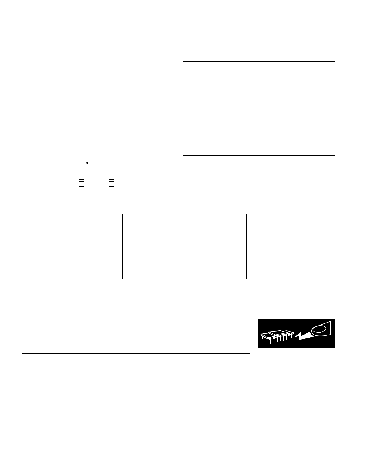
8-Lead SOIC Package
APPLICATIONS
Cellular Base Stations
Communications Receivers
RF/IF Gain Block
Differential A-to-D Driver
SAW Filter Interface
Single-Ended to Differential Conversion
High Performance Video
High Speed Data Transmission
1.0 GHz Differential Amplifier
AD8350
FUNCTIONAL BLOCK DIAGRAMS
8-Lead SOIC Package (with Enable)
PRODUCT DESCRIPTION
The AD8350 series are high performance fully-differential
amplifiers useful in RF and IF circuits up to 1000 MHz. The
amplifier has excellent noise figure of 5.9 dB at 250 MHz. It
offers a high output third order intercept (OIP3) of +22dBm
at 250 MHz. Gain versions of 15 dB and 20 dB are offered.
The AD8350 is designed to meet the demanding performance
requirements of communications transceiver applications. It
enables a high dynamic range differential signal chain, with
exceptional linearity and increased common-mode rejection.
The device can be used as a general purpose gain block, an
A-to-D driver, and high speed data interface driver, among
other functions. The AD8350 input can also be used as a singleended-to-differential converter.
The amplifier can be operated down to +5 V with an OIP3 of
+22 dBm at 250 MHz and slightly reduced distortion performance. The wide bandwidth, high dynamic range and temperature stability make this product ideal for the various RF and IF
frequencies required in cellular, CATV, broadband, instrumentation and other applications.
The AD8350 is offered in an 8-lead single SOIC package. It
operates from +5 V and +10 V power supplies, drawing 28 mA
typical. The AD8350 offers a power enable function for powersensitive applications. The AD8350 is fabricated using Analog
Devices’ proprietary high speed complementary bipolar process.
The device is available in the industrial (–40°C to +85°C)
temperature range.
REV. 0
Information furnished by Analog Devices is believed to be accurate and
reliable. However, no responsibility is assumed by Analog Devices for its
use, nor for any infringements of patents or other rights of third parties
which may result from its use. No license is granted by implication or
otherwise under any patent or patent rights of Analog Devices.
One Technology Way, P.O. Box 9106, Norwood, MA 02062-9106, U.S.A.
Tel: 781/329-4700 World Wide Web Site: http://www.analog.com
Fax: 781/326-8703 © Analog Devices, Inc., 1999
Page 2

(@ +25ⴗC, VS = +5 V, G = 15 dB, unless otherwise noted. All specifications refer
AD8350-15–SPECIFICA TIONS
to differential inputs and differential outputs unless noted.)
Parameter Conditions Min Typ Max Units
DYNAMIC PERFORMANCE
–3 dB Bandwidth VS = +5 V, V
= +10 V, V
V
Bandwidth for 0.1 dB Flatness V
Slew Rate V
Settling Time 0.1%, V
Gain (S21)
1
Gain Supply Sensitivity V
Gain Temperature Sensitivity T
Isolation (S12)
1
S
= +5 V, V
S
V
= +10 V, V
S
= 1 V p-p 2000 V/µs
OUT
OUT
VS = +5 V, f = 50 MHz 14 15 16 dB
= +5 V to +10 V, f = 50 MHz 0.003 dB/V
S
to T
MIN
f = 50 MHz –18 dB
= 1 V p-p 0.9 GHz
OUT
= 1 V p-p 1.1 GHz
OUT
= 1 V p-p 270 MHz
OUT
= 1 V p-p 270 MHz
OUT
= 1 V p-p 10 ns
MAX
–0.002 dB/°C
NOISE/HARMONIC PERFORMANCE
50 MHz Signal
Second Harmonic V
Third Harmonic V
Output Second Order Intercept
Output Third Order Intercept
2
2
= +5 V, V
S
V
= +10 V, V
S
= +5 V, V
S
= +10 V, V
V
S
VS = +5 V 52 dBm
V
= +10 V 52 dBm
S
VS = +5 V 22 dBm
V
= +10 V 23 dBm
S
= 1 V p-p –66 dBc
OUT
= 1 V p-p –67 dBc
OUT
= 1 V p-p –65 dBc
OUT
= 1 V p-p –70 dBc
OUT
250 MHz Signal
Second Harmonic V
Third Harmonic V
Output Second Order Intercept
Output Third Order Intercept
1 dB Compression Point (RTI)
2
2
2
= +5 V, V
S
V
= +10 V, V
S
= +5 V, V
S
= +10 V, V
V
S
VS = +5 V 33 dBm
V
= +10 V 34 dBm
S
VS = +5 V 18 dBm
V
= +10 V 22 dBm
S
VS = +5 V 2 dBm
= +10 V 5 dBm
V
S
= 1 V p-p –48 dBc
OUT
= 1 V p-p –49 dBc
OUT
= 1 V p-p –52 dBc
OUT
= 1 V p-p –61 dBc
OUT
Voltage Noise (RTI) f = 150 MHz 1.7 nV/√Hz
Noise Figure f = 150 MHz 6.8 dB
INPUT/OUTPUT CHARACTERISTICS
Differential Offset Voltage (RTI) V
Differential Offset Drift T
OUT+
MIN
– V
to T
OUT–
MAX
±1mV
0.02 mV/°C
Input Bias Current 15 µA
Input Resistance Real 200 Ω
Input Capacitance 2pF
CMRR f = 50 MHz –67 dB
Output Resistance Real 200 Ω
Output Capacitance 2pF
POWER SUPPLY
Operating Range +4 +11.0 V
Quiescent Current Powered Up, V
Powered Down, V
Powered Up, V
Powered Down, V
= +5 V 25 28 32 mA
S
= +5 V 3 3.8 5.5 mA
S
= +10 V 27 30 34 mA
S
= +10 V 3 4 6.5 mA
S
Power-Up/Down Switching 15 ns
Power Supply Rejection Ratio f = 50 MHz, VS ∆ = 1 V p-p –58 dB
OPERATING TEMPERATURE RANGE –40 +85 °C
NOTES
1
See Tables I–IV for complete list of S-Parameters.
2
Re: 50 Ω.
Specifications subject to change without notice.
–2–
REV. 0
Page 3

(@ +25ⴗC, VS = +5 V, G = 20 dB, unless otherwise noted. All
specifications refer to differential inputs and differential outputs
AD8350-20–SPECIFICATIONS
unless noted.)
AD8350
Parameter Conditions Min Typ Max Units
DYNAMIC PERFORMANCE
–3 dB Bandwidth VS = +5 V, V
V
= +10 V, V
Bandwidth for 0.1 dB Flatness V
Slew Rate V
Settling Time 0.1%, V
Gain (S21)
1
Gain Supply Sensitivity V
Gain Temperature Sensitivity T
Isolation (S12)
1
S
= +5 V, V
S
= +10 V, V
V
S
= 1 V p-p 2000 V/µs
OUT
OUT
VS = +5 V, f = 50 MHz 19 20 21 dB
= +5 V to +10 V, f = 50 MHz 0.003 dB/V
S
to T
MIN
f = 50 MHz –22 dB
= 1 V p-p 0.7 GHz
OUT
= 1 V p-p 0.9 GHz
OUT
= 1 V p-p 230 MHz
OUT
= 1 V p-p 200 MHz
OUT
= 1 V p-p 15 ns
MAX
–0.002 dB/°C
NOISE / HARMONIC PERFORMANCE
50 MHz Signal
Second Harmonic V
Third Harmonic V
Output Second Order Intercept
Output Third Order Intercept
2
2
= +5 V, V
S
V
= +10 V, V
S
= +5 V, V
S
V
= +10 V, V
S
= 1 V p-p –65 dBc
OUT
= 1 V p-p –66 dBc
OUT
= 1 V p-p –66 dBc
OUT
= 1 V p-p –70 dBc
OUT
VS = +5 V 50 dBm
= +10 V 50 dBm
V
S
VS = +5 V 22 dBm
V
= +10 V 23 dBm
S
250 MHz Signal
Second Harmonic V
Third Harmonic V
Output Second Order Intercept
Output Third Order Intercept
1 dB Compression Point (RTI)
2
2
2
= +5 V, V
S
V
= +10 V, V
S
= +5 V, V
S
V
= +10 V, V
S
VS = +5 V 31 dBm
= +10 V 32 dBm
V
S
VS = +5 V 18 dBm
V
= +10 V 22 dBm
S
VS = +5 V –2.6 dBm
V
= +10 V 1.8 dBm
S
= 1 V p-p –45 dBc
OUT
= 1 V p-p –46 dBc
OUT
= 1 V p-p –55 dBc
OUT
= 1 V p-p –60 dBc
OUT
Voltage Noise (RTI) f = 150 MHz 1.7 nV/√Hz
Noise Figure f = 150 MHz 5.6 dB
INPUT/OUTPUT CHARACTERISTICS
Differential Offset Voltage (RTI) V
Differential Offset Drift T
OUT+
MIN
– V
to T
OUT–
MAX
±1mV
0.02 mV/°C
Input Bias Current 15 µA
Input Resistance Real 200 Ω
Input Capacitance 2pF
CMRR f = 50 MHz –52 dB
Output Resistance Real 200 Ω
Output Capacitance 2pF
POWER SUPPLY
Operating Range +4 +11.0 V
Quiescent Current Powered Up, V
Powered Down, V
Powered Up, V
Powered Down, V
= +5 V 25 28 32 mA
S
= +5 V 3 3.8 5.5 mA
S
= +10 V 27 30 34 mA
S
= +10 V 3 4 6.5 mA
S
Power-Up/Down Switching 15 ns
Power Supply Rejection Ratio f = 50 MHz, VS ∆ = 1 V p-p –45 dB
OPERATING TEMPERATURE RANGE –40 +85 °C
NOTES
1
See Tables I–IV for complete list of S-Parameters.
2
Re: 50 Ω.
Specifications subject to change without notice.
REV. 0 –3–
Page 4
AD8350
WARNING!
ESD SENSITIVE DEVICE
ABSOLUTE MAXIMUM RATINGS*
Supply Voltage, VS . . . . . . . . . . . . . . . . . . . . . . . . . . . . +11 V
Input Power Differential . . . . . . . . . . . . . . . . . . . . . . . +8 dBm
Internal Power Dissipation . . . . . . . . . . . . . . . . . . . . .400 mW
. . . . . . . . . . . . . . . . . . . . . . . . . . . . . . . . . . . . . . . 100°C/W
θ
JA
Maximum Junction Temperature . . . . . . . . . . . . . . . . +125°C
Operating Temperature Range . . . . . . . . . . . .–40°C to +85°C
Storage Temperature Range . . . . . . . . . . . . .–65°C to +150°C
Lead Temperature Range (Soldering 60 sec) . . . . . . . . +300°C
*Stresses above those listed under Absolute Maximum Ratings may cause perma-
nent damage to the device. This is a stress rating only; functional operation of the
device at these or any other conditions above those indicated in the operational
section of this specification is not implied. Exposure to absolute maximum rating
conditions for extended periods may effect device reliability.
PIN CONFIGURATION
IN+
ENBL
V
OUT+
CC
1
2
AD8350
TOP VIEW
3
(Not to Scale)
4
8
7
6
5
IN–
GND
GND
OUT–
ORDERING GUIDE
Model Temperature Range Package Description Package Option
AD8350AR15 –40°C to +85°C 8-Lead SOIC SO-8
AD8350AR15-REEL1–40°C to +85°C 8-Lead SOIC SO-8
AD8350AR15-REEL7
2
–40°C to +85°C 8-Lead SOIC SO-8
AD8350AR15-EVAL Evaluation Board (15 dB)
AD8350AR20 –40°C to +85°C 8-Lead SOIC SO-8
AD8350AR20-REEL
AD8350AR20-REEL7
1
–40°C to +85°C 8-Lead SOIC SO-8
2
–40°C to +85°C 8-Lead SOIC SO-8
AD8350AR20-EVAL Evaluation Board (20 dB)
NOTES
1
13" Reels of 2500 each.
2
7" Reels of 750 each.
PIN FUNCTION DESCRIPTIONS
Pin Function Description
1, 8 IN+, IN– Differential Inputs. IN+ and IN–
should be ac-coupled (pins have a dc
bias of midsupply). Differential input
impedance is 200 Ω.
2 ENBL Power-up Pin. A high level (5 V) en-
ables the device; a low level (0 V) puts
device in sleep mode.
3V
CC
Positive Supply Voltage. +5 V to +10V.
4, 5 OUT+, OUT– Differential Outputs. OUT+ and
OUT– should be ac-coupled (pins have
a dc bias of midsupply). Differential
input impedance is 200 Ω.
6, 7 GND Common External Ground Reference.
CAUTION
ESD (electrostatic discharge) sensitive device. Electrostatic charges as high as 4000 V readily
accumulate on the human body and test equipment and can discharge without detection.
Although the AD8350 features proprietary ESD protection circuitry, permanent damage may
occur on devices subjected to high energy electrostatic discharges. Therefore, proper ESD
precautions are recommended to avoid performance degradation or loss of functionality.
–4–
REV. 0
Page 5

Typical Performance Characteristics–
FREQUENCY – MHz
ISOLATION – dB
–10
1
–15
–20
–25
–30
10 100 1k 10k
VCC = 10V
VCC = 5V
AD8350
50
40
30
20
SUPPLY CURRENT – mA
10
0
–40
–20
VCC = 10V
VCC = 5V
0
20 40 60 80
TEMPERATURE – 8C
Figure 1. Supply Current vs.
Temperature
350
300
250
200
IMPEDANCE – V
150
VCC = 10V
VCC = 5V
20
15
10
GAIN – dB
5
0
1
10 100 1k 10k
FREQUENCY – MHz
VCC = 10V
VCC = 5V
Figure 2. AD8350-15 Gain (S21) vs.
Frequency
350
300
250
200
IMPEDANCE – V
150
VCC = 10V
VCC = 5V
25
20
15
GAIN – dB
10
5
1
10 100 1k 10k
VCC = 10V
VCC = 5V
FREQUENCY – MHz
Figure 3. AD8350-20 Gain (S21) vs.
Frequency
500
400
300
200
IMPEDANCE – V
100
VCC = 10V
VCC = 5V
100
1
10 100 1k
FREQUENCY – MHz
Figure 4. AD8350-15 Input Imped ance vs. Frequency
500
400
300
200
IMPEDANCE – V
100
0
1
10 100 1k
FREQUENCY – MHz
VCC = 5V
VCC = 10V
Figure 7. AD8350-20 Output Impedance vs. Frequency
100
1
10 100 1k
FREQUENCY – MHz
Figure 5. AD8350-20 Input Impedance vs. Frequency
–5
–10
–15
ISOLATION – dB
–20
–25
1
10 100 1k 10k
FREQUENCY – MHz
VCC = 10V
VCC = 5V
Figure 8. AD8350-15 Isolation (S12)
vs. Frequency
0
1
10 100 1k
FREQUENCY – MHz
Figure 6. AD8350-15 Output Impedance vs. Frequency
Figure 9. AD8350-20 Isolation (S12)
vs. Frequency
REV. 0
–5–
Page 6

AD8350
p
FREQUENCY – MHz
1dB COMPRESSION – dBm (Re: 50V)
0
100 200 300 400 500 600
7.5
5.0
2.5
0
–2.5
–5.0
VCC = 10V
VCC = 5V
INPUT REFERRED
10.0
–40
V
= 1V p-p
OUT
–45
–50
–55
–60
–65
DISTORTION – dBc
–70
–75
–80
0
50 100 150 200 250 300
FUNDAMENTAL FREQUENCY – MHz
HD2 (VCC = 10V)
HD2 (VCC = 5V)
HD3 (VCC = 5V)
HD3 (VCC = 10V)
Figure 10. AD8350-15 Harmonic
Distortion vs. Frequency
–45
FO = 50MHz
–55
–65
DISTORTION – dBc
–75
HD2 (VCC = 5V)
HD3 (VCC = 5V)
HD2 (VCC = 10V)
HD3 (VCC = 10V)
–40
V
= 1V p-p
OUT
–45
–50
–55
–60
–65
DISTORTION – dBc
–70
–75
–80
0
HD2 (VCC = 5V)
HD2 (VCC = 10V)
HD3 (VCC = 5V)
HD3 (VCC = 10V)
50 100 150 200 250 300
FUNDAMENTAL FREQUENCY – MHz
Figure 11. AD8350-20 Harmonic
Distortion vs. Frequency
60
55
50
45
40
OIP2 – dBm (Re: 50V)
35
VCC = 10V
VCC = 5V
–45
FO = 50MHz
HD3 (VCC = 5V)
HD2 (VCC = 5V)
–55
–65
DISTORTION – dBc
–75
–85
0
0.5 1 1.5 2 2.5 3 3.5
OUTPUT VOLTAGE – V p-p
HD2 (VCC = 10V)
HD3 (VCC = 10V)
Figure 12. AD8350-15 Harmonic Distortion vs. Differential Output Voltage
60
55
50
45
40
OIP2 – dBm (Re: 50V)
35
VCC = 10V
VCC = 5V
–85
0
0.5 1 1.5 2 2.5 3 3.5
OUTPUT VOLTAGE – V p-
Figure 13. AD8350-20 Harmonic Distortion vs. Differential Output Voltage
35
30
25
20
15
OIP3 – dBm (Re: 50V)
10
5
0
50 100 150 200 250 300
VCC = 10V
VCC = 5V
FREQUENCY – MHz
Figure 16. AD8350-15 Output
Referred IP3 vs. Frequency
30
0
50 100 150 200 250 300
FREQUENCY – MHz
Figure 14. AD8350-15 Output
Referred IP2 vs. Frequency
35
30
25
20
15
OIP3 – dBm (Re: 50V)
10
5
0
50 100 150 200 250 300
VCC = 10V
VCC = 5V
FREQUENCY – MHz
Figure 17. AD8350-20 Output
Referred IP3 vs. Frequency
30
0
50 100 150 200 250 300
FREQUENCY – MHz
Figure 15. AD8350-20 Output
Referred IP2 vs. Frequency
Figure 18. AD8350-15 1 dB Compression vs. Frequency
–6–
REV. 0
Page 7

AD8350
7.5
)
V
5.0
2.5
0
–2.5
–5.0
1dB COMPRESSION – dBm (Re: 50
–7.5
0
VCC = 5V
100 200 300 400 500 600
FREQUENCY – MHz
INPUT REFERRED
VCC = 10V
Figure 19. AD8350-20 1 dB Compression vs. Frequency
25
20
15
10
5
0
GAIN – dB
–5
–10
–15
–20
1
2345678910
VCC – Volts
AD8350-20
AD8350-15
Figure 22. AD8350 Gain (S21) vs.
Supply Voltage
10
9
8
7
NOISE FIGURE – dB
6
5
0
VCC = 10V
VCC = 5V
50 100 150 200 250 300 350 400 450 500
FREQUENCY – MHz
Figure 20. AD8350-15 Noise Figure
vs. Frequency
100
50
0
–50
–100
–150
OUTPUT OFFSET – mV
–200
–250
–40
–20
V
+ (VCC = 5V)
OUT
V
– (VCC = 5V)
OUT
V
+ (VCC = 10V)
OUT
V
– (VCC = 10V)
OUT
0
20 40 60 80
TEMPERATURE – 8C
Figure 23. AD8350 Output Offset
Voltage vs. Temperature
10
9
8
7
NOISE FIGURE – dB
6
5
0
50 100 150 200 250 300 350 400 450 500
VCC = 10V
VCC = 5V
FREQUENCY – MHz
Figure 21. AD8350-20 Noise Figure
vs. Frequency
–20
VCC = 5V
–30
–40
–50
–60
PSRR – dB
–70
–80
–90
AD8350-20
AD8350-15
1
10 100 1k
FREQUENCY – MHz
Figure 24. AD8350 PSRR vs.
Frequency
–20
VCC = 5V
–30
–40
–50
–60
PSRR – dB
–70
–80
–90
1
AD8350-20
AD8350-15
10 100 1k
FREQUENCY – MHz
Figure 25. AD8350 CMRR vs.
Frequency
REV. 0
VCC = 5V
30ns
500mV
V
ENBL
OUT
5V
Figure 26. AD8350 Power-Up/Down
Response Time
–7–
Page 8

AD8350
APPLICATIONS
Using the AD8350
Figure 27 shows the basic connections for operating the AD8350.
A single supply in the range +5 V to +10 V is required. The
power supply pin should be decoupled using a 0.1µF capacitor.
The ENBL pin is tied to the positive supply or to +5V (when
= +10 V) for normal operation and should be pulled to
V
CC
ground to put the device in sleep mode. Both the inputs and the
outputs have dc bias levels at midsupply and should be ac-coupled.
Also shown, in Figure 27, are the impedance balancing requirements, either resistive or reactive, of the input and output. With
an input and output impedance of 200 Ω, the AD8350 should
be driven by a 200 Ω source and loaded by a 200 Ω impedance.
A reactive match can also be implemented.
Figure 28 shows how the AD8350 can be driven by a singleended source. The unused input should be ac-coupled to
ground. When driven single-ended, there will be a slight imbalance in the differential output voltages. This will cause an increase in the second order harmonic distortion (at 50 MHz,
with V
= +10 V and V
CC
= 1 V p-p, –59 dBc was measured
OUT
for the second harmonic on AD8350-15).
Reactive Matching
In practical applications, the AD8350 will most likely be matched
using reactive matching components as shown in Figure 29.
Matching components can be calculated using a Smith Chart
and the AD8350’s S-Parameters (see Tables I and II) along
with those of the devices that are driving and loading it. The SParameters in Tables I and II assume a differential source and
load impedance of 50 Ω. Because the load impedance on the
output of the AD8350 affects the input impedance, a simultaneous conjugate match must be performed to correctly match
both input and output.
C1
7
8
5
6
AD8350
L1 L2
C1
ENBL (+5V)
–
+
1
3
2
+VS (+5V TO +10V)
4
C2
0.1mF
C2
C2
Figure 29. Reactively Matching the Input and Output
SOURCE
Z = 100V
C2
0.001mF
7
8
6
C4
5
0.001mF
AD8350
–
+
1
3
2
Z = 100V
C1
0.001mF
ENBL (+5V)
+V
S
4
C5
0.1mF
(+5V TO +10V)
C3
0.001mF
Figure 27. Basic Connections for Differential Drive
C5
0.1mF
C4
0.001mF
C3
0.001mF
SOURCE
Z = 200V
C2
0.001mF
C1
0.001mF
ENBL (+5V)
7
8
AD8350
–
1
2
(+5V TO +10V)
+V
S
6
5
+
3
4
LOAD
Z = 200V
LOAD
Z = 200V
Figure 28. Basic Connections for Single-Ended Drive
–8–
REV. 0
Page 9

AD8350
Figure 30 shows how the AD8350 input can be matched for a
single-ended drive. The unused input is ac-coupled to ground
using a low impedance (i.e., high value) capacitance. The SParameters for this configuration are shown in Tables III and
IV. These values assume a single-ended source impedance of
50 Ω and a differential load impedance of 50 Ω. As in the case
of a differential drive, a simultaneous conjugate match must be
performed to correctly match both input and output.
0.001mF
7
8
5
6
AD8350
–
+
1
3
2
4
C1
L1
ENBL
(+5V)
+V
(+5V TO +10V)
S
C2
0.1mF
C2
L2
C2
Figure 30. Matching Circuit for Single-Ended Drive
C1
0.001mF
Evaluation Board
Figure 31 shows the schematic of the AD8350 evaluation board
as it is shipped from the factory. The board is configured to
allow easy evaluation using single-ended 50 Ω test equipment.
The input and output transformers have a 4-to-1 impedance
ratio and transform the AD8350’s 200Ω input and output
impedances to 50 Ω. In this mode, 0 Ω resistors (R1 and R4)
are required.
To allow compensation for the insertion loss of the transformers, a calibration path is provided at Test In and Test Out. This
consists of two transformers connected back to back.
To drive and load the board differentially, transformers T1 and
T2 should be removed and replaced with four 0Ω resistors
(0805 size); Resistors R1 and R4 (0 Ω) should also be removed.
This yields a circuit with a broadband input and output impedance of 200 Ω. To match to impedances other than this, matching components (0805 size) can be placed on pads C1, C2, C3,
C4, L1 and L2.
C3
0.001mF
IN–
IN+
R1
T1: TC4-1W
0V
(MINI CIRCUITS)
61
TEST IN
7
6
+
3
2
+V
S
(MINI CIRCUITS)
5
4
C5
0.1mF
T4: TC4-1W
16
R2
0V
(OPEN)
C2
0.001mF
+V
L1
A
3
S
2
B
T3: TC4-1W
(MINI CIRCUITS)
61
8
AD8350
1
SW1
1
–
Figure 31. AD8350 Evaluation Board
L2
(OPEN)
C4
0.001mF
R3
0V
TEST OUT
T2: TC4-1W
(MINI CIRCUITS)
1
6
R4
0V
OUT–
OUT+
REV. 0
–9–
Page 10

AD8350
Table I. Typical S Parameters AD8350-15: VCC = 5 V, Differential Input Signal.
Z
(diff) = 50 ⍀, Z
SOURCE
(diff) = 50 ⍀
LOAD
Frequency
(MHz) S11 S12 S21 S22
50 0.791 ∠ –3° 0.068 ∠ 177° 2.73 ∠ –3° 0.795 ∠ –2°
100 0.787 ∠ –6° 0.071 ∠ 174° 2.79 ∠ –7° 0.794 ∠ –5°
150 0.778 ∠ –9° 0.070 ∠ 172° 2.91 ∠ –11° 0.787 ∠ –7°
200 0.766 ∠ –13° 0.072 ∠ 168° 3.06∠ –16° 0.779 ∠ –10°
250 0.749 ∠ –17° 0.074 ∠ 165° 3.24∠ –21° 0.768 ∠ –12°
Table II. Typical S Parameters AD8350-20: VCC = 5 V, Differential Input Signal.
Z
SOURCE
(diff) = 50 ⍀, Z
(diff) = 50 ⍀
LOAD
Frequency
(MHz) S11 S12 S21 S22
50 0.810 ∠ –4° 0.046 ∠ 176° 4.82 ∠ –2.5° 0.822 ∠ –3°
100 0.795 ∠ –8° 0.043 ∠ 173° 4.99 ∠ –6.16° 0.809 ∠ –5°
150 0.790 ∠ –12° 0.045 ∠ 169° 5.30∠ –9.82 ° 0.807 ∠ –8°
200 0.776 ∠ –17° 0.046 ∠ 165° 5.71∠ –14.89 ° 0.795 ∠ –10°
250 0.757 ∠ –22° 0.048 ∠ 162° 6.25∠ –21.29 ° 0.783 ∠ –13°
Table III. Typical S Parameters AD8350-15: VCC = 5 V, Single-Ended Input Signal.
Z
SOURCE
(diff) = 50 ⍀, Z
(diff) = 50 ⍀
LOAD
Frequency
(MHz) S11 S12 S21 S22
50 0.718 ∠ –6° 0.068 ∠ 177° 2.62 ∠ –4° 0.798 ∠ –3°
100 0.701 ∠ –12° 0.066 ∠ 173° 2.66 ∠ –10° 0.794 ∠ –6°
150 0.683 ∠ –19° 0.067 ∠ 167° 2.76∠ –15° 0.789 ∠ –10°
200 0.657 ∠ –24° 0.069 ∠ 163° 2.86∠ –22° 0.776 ∠ –13°
250 0.625 ∠ –31° 0.070 ∠ 159° 2.98∠ –28° 0.763 ∠ –16°
Table IV. Typical S Parameters AD8350-20: VCC = 5 V, Single-Ended Input Signal.
Z
SOURCE
(diff) = 50 ⍀, Z
(diff) = 50 ⍀
LOAD
Frequency
(MHz) S11 S12 S21 S22
50 0.747 ∠ –7° 0.040 ∠ 175° 4.71 ∠ –4° 0.814 ∠ –3°
100 0.739 ∠ –14° 0.042 ∠ 170° 4.82 ∠ –9° 0.813 ∠ –6°
150 0.728 ∠ –21° 0.044 ∠ 166° 5.08∠ –15° 0.804 ∠ –10°
200 0.698 ∠ –29° 0.045 ∠ 161° 5.37 ∠ –22° 0.792 ∠ –13 °
250 0.659 ∠ –37° 0.048 ∠ 156 ° 5.76 ∠ –30° 0.774 ∠ –16°
–10–
REV. 0
Page 11

0.1574 (4.00)
0.1497 (3.80)
PIN 1
0.0098 (0.25)
0.0040 (0.10)
SEATING
OUTLINE DIMENSIONS
Dimensions shown in inches and (mm).
8-Lead Plastic SOIC
(SO-8)
0.1 968 (5.00)
0.1 890 (4.80)
85
0.0500 (1.27)
PLANE
0.2440 (6.20)
0.2284 (5.80)
41
BSC
0.0192 (0.49)
0.0138 (0.35)
0.0688 (1.75)
0.0532 (1.35)
0.0098 (0.25)
0.0075 (0.19)
0.0196 (0.50)
0.0099 (0.25)
88
0.0500 (1.27)
08
0.0160 (0.41)
AD8350
C3577–8–4/99
3 458
REV. 0
PRINTED IN U.S.A.
–11–
 Loading...