

Page 1
250 MHz–1000 MHz
a
FEATURES
250 MHz–1000 MHz Operating Frequency
+2.5 dBm P1 dB @ 800 MHz
–155 dBm/Hz Noise Floor
0.5 Degree RMS Phase Error (IS95)
0.2 dB Amplitude Balance
Single 2.7 V–5.5 V Supply
Pin-Compatible with AD8346
16-Lead Exposed Paddle TSSOP Package
APPLICATIONS
Cellular Communication Systems
W-CDMA/CDMA/GSM/PCS/ISM Transceivers
Fixed Broadband Access Systems LMDS/MMDS
Wireless LAN
Wireless Local Loop
Digital TV/CATV Modulators
Single Sideband Upconverter
Quadrature Modulator
AD8345
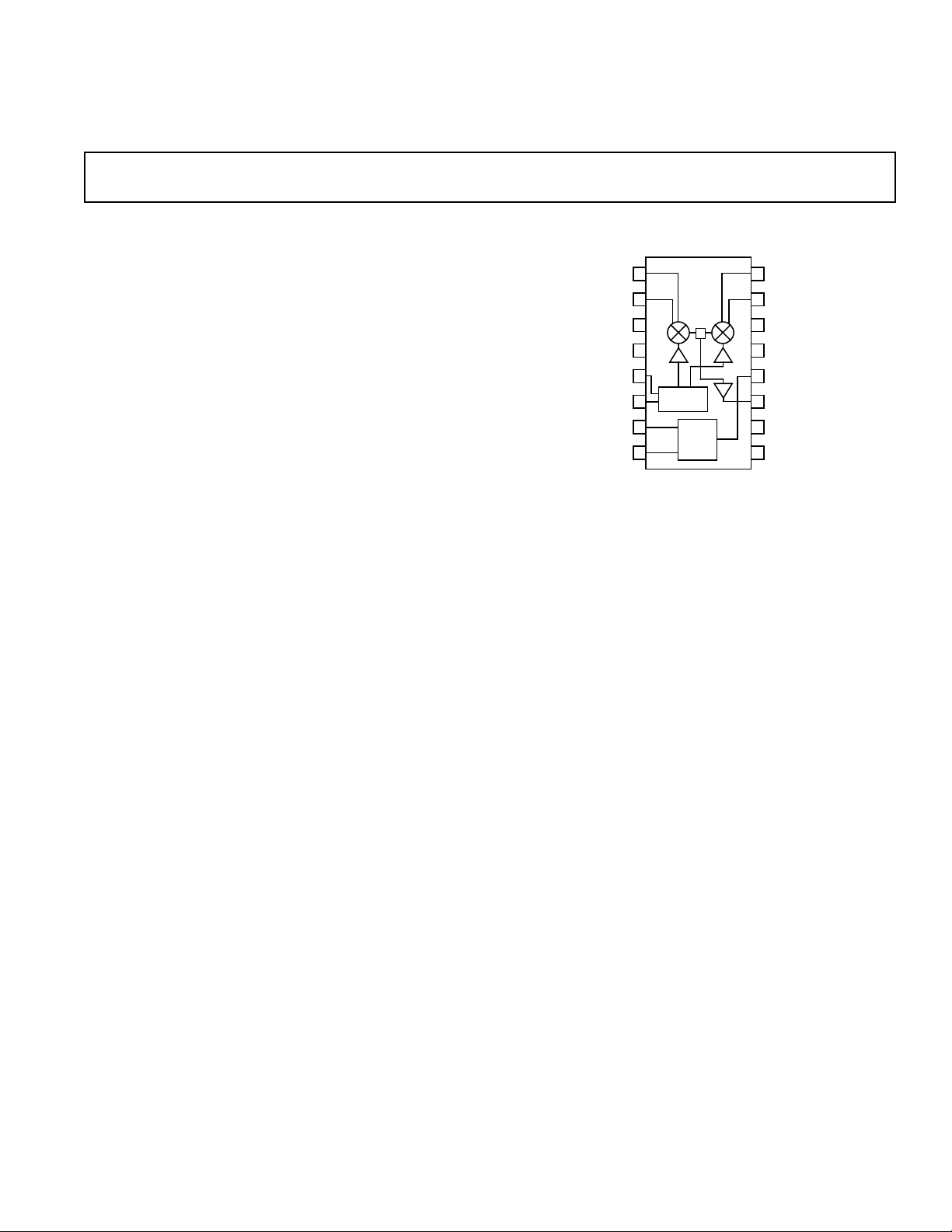
FUNCTIONAL BLOCK DIAGRAM
IBBP
IBBN
COM3
COM1
LOIN
LOIP
VPS1
ENBL
1
2
3
4
5
6
7
8
AD8345
PHASE
SPLITTER
BIAS
+
16
15
14
13
12
11
10
9
QBBP
QBBN
COM3
COM3
VPS2
VOUT
COM2
COM3
PRODUCT DESCRIPTION
The AD8345 is a silicon RFIC quadrature modulator, designed
for use from 250 MHz to 1000 MHz. Its excellent phase accuracy and amplitude balance enable the high performance direct
modulation of an IF carrier.
The AD8345 accurately splits the external LO signal into two
quadrature components through the polyphase phase-splitter
network. The two I and Q LO components are mixed with the
baseband I and Q differential input signals. Finally, the outputs
of the two mixers are combined in the output stage to provide a
single-ended 50 Ω drive at VOUT.
APPLICATIONS
The AD8345 Modulator can be used as the IF transmit modulator in digital communication systems such as GSM and PCS
transceivers. It can also directly modulate an LO signal to
produce QPSK and various QAM formats for 900 MHz communication systems as well as digital TV and CATV systems.
Additionally, this quadrature modulator can be used with direct
digital synthesizers in hybrid phase-locked loops to generate
signals over a wide frequency range with millihertz resolution.
The AD8345 Modulator is supplied in a 16-lead TSSOP package with exposed paddle. Its performance is specified over a
–40°C to +85°C temperature range. This device is fabricated on
Analog Devices’ advanced silicon bipolar process.
REV. 0
Information furnished by Analog Devices is believed to be accurate and
reliable. However, no responsibility is assumed by Analog Devices for its
use, nor for any infringements of patents or other rights of third parties that
may result from its use. No license is granted by implication or otherwise
under any patent or patent rights of Analog Devices.
One Technology Way, P.O. Box 9106, Norwood, MA 02062-9106, U.S.A.
Tel: 781/329-4700 www.analog.com
Fax: 781/326-8703 © Analog Devices, Inc., 2001
Page 2

AD8345–SPECIFICATIONS
(VS = 5 V; LO= –2 dBm @ 800 MHz, 50 ⍀ source and load impedances, I and Q inputs
0.7 V ⴞ 0.3 V on each side for a 1.2 V p-p differential input, I and Q inputs driven in quadrature @ 1 MHz Baseband Frequency.
TA = 25ⴗC, unless otherwise noted.)
Parameters Conditions Min Typ Max Unit
RF OUTPUT
Operating Frequency
1
250 1000 MHz
Output Power –3 –1 +2 dBm
Output P1 dB 2.5 dBm
Noise Floor 20 MHz Offset from LO, All BB –155 dBm/Hz
Inputs at 0.7 V
Quadrature Error (CDMA IS95 Setup, Refer to Figure 13) 0.5 Degree rms
I/Q Amplitude Balance (CDMA IS95 Setup, Refer to Figure 13) 0.2 dB
LO Leakage –42 –33 dBm
Sideband Rejection –42 –34 dBc
Third Order Distortion –52 dBc
Second
Order Distortion –60 dBc
Equivalent Output IP3 25 dBm
Equivalent Output IP2 59 dBm
Output Return Loss (S22) –20 dB
RESPONSE TO CDMA IS95 (Refer to Figure 13)
BASEBAND SIGNALS
ACPR –72 dBc
EVM 1.3 %
Rho 0.9995
LO INPUT
LO Drive level –10 –2 0 dBm
LOIP Input Return Loss (S11)
2
No Termination on LOIP, LOIN at –5 dB
AC Ground
50 Ω Terminating Resistor, Differential –9 dB
Drive via Balun
BASEBAND INPUTS
Input Bias Current 10 µA
Input Capacitance 2pF
DC Common Level 0.6 0.7 0.8 V
Bandwidth (3 dB) Full Power (0.7 V ± 0.3 V on Each 80 MHz
Input, Refer to TPC 2)
ENABLE
Turn-On Enable High to Output within 0.5 dB of 2.5 µs
Final Value
Turn-Off Enable Low to Supply Current Dropping 1.5 µs
below 2 mA
ENBL High Threshold (Logic 1) +V
/2 V
S
ENBL Low Threshold (Logic 0) +VS/2 V
POWER SUPPLIES
Voltage 2.7 5.5 V
Current Active 50 65 78 mA
Current Standby 70 µA
NOTES
1
For information on operation below 250 MHz, see Figure 4.
2
See LO Drive section for more details on input matching.
Specifications subject to change without notice.
–2–
REV. 0
Page 3
AD8345
16
15
14
13
12
11
10
9
QBBP
QBBN
COM3
COM3
VPS2
VOUT
COM2
COM3
1
2
3
4
5
6
7
8
IBBP
IBBN
COM3
COM1
LOIN
LOIP
VPS1
ENBL
AD8345
TOP VIEW
(Not to Scale)
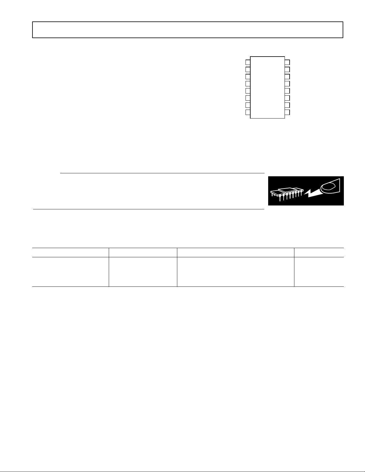
ABSOLUTE MAXIMUM RATINGS*
PIN CONFIGURATION
Supply Voltage VPS1, VPS2 . . . . . . . . . . . . . . . . . . . . . 5.5 V
Input Power LOIP, LOIN (re 50 Ω) . . . . . . . . . . . . . 10 dBm
IBBP, IBBN, QBBP, QBBN . . . . . . . . . . . . . . . . . 0 V, 2.5 V
Internal Power Dissipation . . . . . . . . . . . . . . . . . . . . 500 mW
(Exposed Paddle Soldered Down) . . . . . . . . . . . . 30°C/W
θ
JA
(Exposed Paddle not Soldered Down) . . . . . . . . . 95°C/W
θ
JA
Maximum Junction Temperature . . . . . . . . . . . . . . . . 150°C
Operating Temperature Range . . . . . . . . . . . –40°C to +85°C
Storage Temperature Range . . . . . . . . . . . . –65°C to +150°C
Lead Temperature Range (Soldering 60 sec) . . . . . . . . 300°C
*Stresses above those listed under Absolute Maximum Ratings may cause perma-
nent damage to the device. This is a stress rating only; functional operation of the
device at these or any other conditions above those indicated in the operational
section of this specification is not implied. Exposure to absolute maximum rating
conditions for extended periods may affect device reliability.
CAUTION
ESD (electrostatic discharge) sensitive device. Electrostatic charges as high as 4000 V readily
accumulate on the human body and test equipment and can discharge without detection. Although
the AD8345 features proprietary ESD protection circuitry, permanent damage may occur on
devices subjected to high-energy electrostatic discharges. Therefore, proper ESD precautions are
recommended to avoid performance degradation or loss of functionality.
WARNING!
ESD SENSITIVE DEVICE
ORDERING GUIDE
Model Temperature Range Package Description Package Option
AD8345ARE –40°C to +85°C Tube (16-Lead TSSOP with Exposed Pad) RE-16
AD8345ARE-REEL 13" Tape and Reel
AD8345ARE-REEL7 7" Tape and Reel
AD8345-EVAL Evaluation Board
REV. 0
–3–
Page 4
AD8345
PIN FUNCTION DESCRIPTIONS
Equivalent
Pin No. Mnemonic Function Circuit
1, 2 IBBP, IBBN I Channel Baseband Differential Input Pins. These high impedance inputs should Circuit A
be dc biased to approximately 0.7 V. Nominal characterized ac swing is 0.6 V p-p
on each pin (0.4 V to 1 V). This gives a differential drive of 1.2 V p-p. Inputs are
not self-biasing so external biasing circuitry must be used in ac-coupled applications.
3, 9, 13, 14 COM3 Ground Pin for Input V-to-I Converters and Mixer Core.
4 COM1 Ground Pin for the LO Phase-Splitter and LO Buffers.
5, 6 LOIN, LOIP Differential LO Drive Pins. Internal dc bias (approximately 1.8 V @ V
is supplied. Pins must be ac-coupled. Single-ended or differential drive is permissible.
7 VPS1 Power Supply Pin for the Bias Cell and LO Buffers. This pin should be decoupled
using local 1000 pF and 0.01 µF capacitors.
8 ENBL Enable Pin. A high level enables the device; a low level puts the device in sleep mode. Circuit C
10 COM2 Ground Pin for the Output Stage of Output Amplifier.
11 VOUT 50 Ω DC-Coupled RF Output. Pin should be ac-coupled. Circuit D
12 VPS2 Power supply pin for baseband input voltage to current converters and mixer core.
This pin should be decoupled using local 1000 pF and 0.01 µF capacitors.
15, 16 QBBN, QBBP Q Channel Baseband Differential Input Pins. Inputs should be dc biased to Circuit A
approximately 0.7 V. Nominal characterized ac swing is 0.6 V p-p on each pin
(0.4 V to 1 V). This gives a differential drive level of 1.2 V p-p. Inputs are not
self-biasing so external biasing circuitry must be used in ac-coupled applications.
= 5 V) Circuit B
S
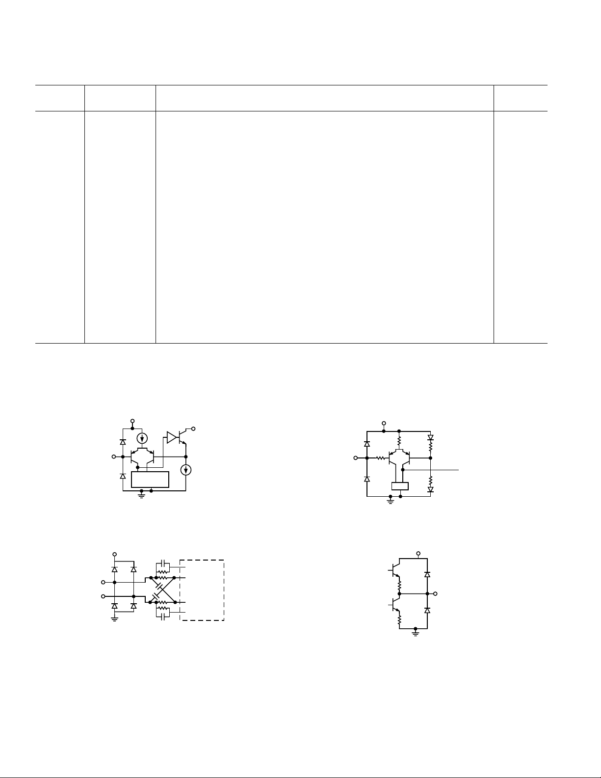
EQUIVALENT CIRCUITS
VPS2
INPUT
CURRENT
MIRROR
Circuit A
VPS1
LOIN
LOIP
Circuit B
BUFFER
TO MIXER
CORE
PHASE
SPLITTER
CONTINUES
Figure 1. Equivalent Circuits
ENBL
VPS2
100k⍀
Circuit C
VPS2
40⍀
40⍀
Circuit D
100k⍀
100k⍀
VOUT
TO BIAS FOR
STARTUP/
SHUTDOWN
–4–
REV. 0
Page 5
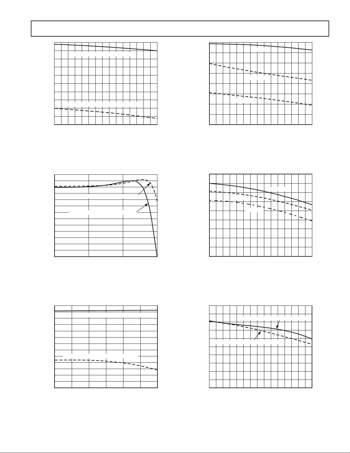
Typical Performance Characteristics–
AD8345
0
–2
–4
–6
–8
–10
–12
SSB POWER – dBm
–14
–16
–18
–20
250
V
= 5V, DIFFERENTIAL INPUT = 1.2V p-p
S
VS = 2.7V, DIFFERENTIAL INPUT = 200mV p-p
300 350 400 450 500 550 600 650 700 750 800 850 900 950 1000
LO FREQUENCY – MHz
TPC 1. Single Sideband (SSB) Output Power (P
Frequency (F
Baseband Frequency (F
1.0
0.5
0.0
–0.5
–1.0
–1.5
–2.0
–2.5
–3.0
–3.5
–4.0
OUTPUT POWER VARIATION – dB
–4.5
–5.0
–5.5
). (I and Q Inputs Driven in Quadrature at
LO
VS = 2.7V, 5V DIFFERENTIAL INPUT = 200mV p-p
V
= 5V, DIFFERENTIAL INPUT = 1.2V p-p
S
0.1
) = 1 MHz; TA = 25°C)
BB
1 10 100
BASEBAND FREQUENCY – MHz
OUT
) vs. LO
0
TA = –40ⴗC
TA = +25ⴗC
500 800
LO FREQUENCY – MHz
–10
–12
SSB OUTPUT P1dB – dBm
–14
–16
–2
–4
–6
–8
TA = +85ⴗC
350 650 950300 400 450 550 600 700 750 850 900 1000
250
TPC 4. SSB Output 1 dB Compression Point (OP 1 dB) vs.
F
. (VS = 2.7 V, LO Level = –2 dBm, I and Q Inputs Driven
LO
in Quadrature, F
4.0
3.5
3.0
2.5
2.0
1.5
1.0
SSB OUTPUT P1dB – dBm
0.5
0.0
–0.5
250
= 1 MHz)
BB
TA = +85ⴗC
TA = +25ⴗC
TA = –40ⴗC
350 650 950300 400 450 550 600 700 750 850 900 1000
500 800
LO FREQUENCY – MHz
TPC 2. I and Q Input Bandwidth. (TA = 25°C, FLO = 800 MHz,
LO Level = –2 dBm, I and Q Inputs Driven in Quadrature)
0
–2
–4
–6
–8
–10
–12
–14
–16
SSB POWER – dBm
–18
–20
–22
–24
–26
TPC 3. SSB P
V
= 2.7V, DIFFERENTIAL INPUT = 200mV p-p
S
–40
–20 20 60
OUT
Level = –2 dBm, F
VS = 5V, DIFFERENTIAL INPUT = 1.2V p-p
04080
TEMPERATURE – ⴗC
vs. Temperature. (FLO = 800 MHz, LO
= 1 MHz, I and Q Inputs Driven in
BB
Quadrature)
REV. 0
TPC 5. SSB Output 1 dB Compression Point (OP 1 dB) vs.
F
. (VS = 5 V, LO Level = –2 dBm, I and Q Inputs Driven in
LO
Quadrature, F
–40
–41
–42
–43
–44
–45
–46
–47
–48
CARRIER FEEDTHROUGH – dBm
–49
–50
= 1 MHz)
BB
VS = 5V, DIFFERENTIAL INPUT = 1.2V p-p
VS = 2.7V, DIFFERENTIAL INPUT = 200mV p-p
350 650 950300 400 450 550 600 700 750 850 900 1000
250
500 800
LO FREQUENCY – MHz
TPC 6. Carrier Feedthrough vs. FLO. (LO Level = –2 dBm,
= 25°C)
T
A
–5–
Page 6

AD8345
–30
–32
–34
–36
–38
–40
–42
–44
–46
CARRIER FEEDTHROUGH – dBm
–48
–50
–40
VS = 5V, DIFFERENTIAL INPUT = 1.2V p-p
VS = 2.7V, DIFFERENTIAL INPUT = 200mV p-p
–20 20 40 60 80
0
TEMPERATURE – ⴗC
TPC 7. Carrier Feedthrough vs. Temperature.
(F
= 800 MHz, LO Level = –2 dBm)
LO
30
28
T = +85
26
T = –40
24
22
20
18
16
14
12
PERCENTAGE
10
8
6
4
2
0
–86
–82 –78 –74 –70 –66 –62 –58 –54 –50
CARRIER FEEDTHROUGH – dBm
AFTER NULLING TO ⬍–65dBm AT +25ⴗC
TPC 8. Carrier Feedthrough Distribution at Temperature
Extremes. After Feedthrough Nulled to <–65 dBm at T
°
C. (FLO = 800 MHz, LO Level = –2 dBm)
25
=
A
–26
–28
= 5V, DIFFERENTIAL INPUT = 1.2V p-p
V
S
–30
–32
–34
–36
–38
–40
SIDEBAND SUPPRESSION – dBc
–42
VS = 2.7V, DIFFERENTIAL INPUT = 200mV p-p
–44
BASEBAND FREQUENCY – MHz
454035302520151050
50
TPC 10. Sideband Suppression vs. FBB. (TA = 25°C,
= 800 MHz, LO Level = –2 dBm, I and Q Inputs
F
LO
Driven in Quadrature)
–35
–36
–37
–38
–39
–40
–41
–42
–43
SIDEBAND SUPPRESSION – dBc
–44
–45
VS = 2.7V, DIFFERENTIAL INPUT = 200mV p-p
VS = 5V, DIFFERENTIAL INPUT = 1.2V p-p
6040200–20–40
TEMPERATURE – ⴗC
80
TPC 11. Sideband Suppression vs. Temperature.
(F
= 800 MHz, LO Level = –2 dBm, FBB =1 MHz,
LO
I and Q Inputs Driven in Quadrature)
–30
–32
–34
VS = 2.7V, DIFFERENTIAL INPUT = 200mV p-p
–36
–38
–40
–42
–44
–46
SIDEBAND SUPPRESSION – dBc
–48
–50
V
= 5V, DIFFERENTIAL INPUT = 1.2V p-p
S
LO FREQUENCY – MHz
950900850800750700650600550500450400350300250
1000
TPC 9. Sideband Suppression vs. FLO. (TA = 25°C,
LO Level = –2 dBm, F
= 1 MHz, I and Q Inputs
BB
Driven in Quadrature)
–6–
–20
–25
VS = 5V, DIFFERENTIAL INPUT = 1.2V p-p
–30
–35
–40
–45
–50
–55
THIRD ORDER DISTORTION – dBc
–60
–65
0
5 101520253035404550
VS = 2.7V, DIFFERENTIAL INPUT = 200mV p-p
BASEBAND FREQUENCY – MHz
TPC 12. Third Order Distortion vs. FBB. (TA = 25°C,
= 800 MHz, LO Level = –2 dBm, I and Q Inputs
F
LO
Driven in Quadrature)
REV. 0
Page 7

AD8345
–45
–50
–55
VS = 5V, DIFFERENTIAL INPUT = 1.2V p-p
–60
–65
–70
THIRD ORDER DISTORTION – dBc
–75
–80
VS = 2.7V, DIFFERENTIAL INPUT = 200mV p-p
TEMPERATURE – ⴗC
6040200–20–40
TPC 13. Third Order Distortion vs. Temperature.
= 800 MHz, LO Level = –2 dBm, FBB =1 MHz,
(F
LO
I and Q Inputs Driven in Quadrature)
–10
–15
–20
–25
–30
–35
–40
–45
–50
–55
THIRD ORDER DISTORTION – dBc
–60
–65
–70
BASEBAND DIFFERENTIAL INPUT VOLTAGE – V p-p
TPC 14. Third Order Distortion and SSB P
band Differential Input Level. (T
LO Level = –2 dBm, F
SSB P
OUT
THIRD ORDER DISTORTION
= 25°C, FLO = 800 MHz,
= 1 MHz, VS = 2.7 V)
BB
A
OUT
80
–2
–4
–6
–8
–10
–12
–14
–16
–18
–20
–22
–24
–26
3.02.52.01.51.00.50.0
vs. Base-
SSB OUTPUT POWER – dBm
80
75
70
VS = 5V, DIFFERENTIAL INPUT = 1.2V p-p
65
60
55
SUPPLY CURRENT – mA
50
45
40
–40
VS = 2.7V, DIFFERENTIAL INPUT = 200mV p-p
–20 20 40 60 80
0
TEMPERATURE – ⴗC
TPC 16. Power Supply Current vs. Temperature
1GHz
SMITH CHART
NORMALIZED
WITH 50⍀
WITH 100⍀
1GHz
TO 50⍀
LOIN NO BALUN
OR TERMINATION
250MHz
TPC 17. Smith Chart of LOIN Port S11 (LOIP Pin ACCoupled to Ground). Curves with Balun and External
Termination Resistors Also Shown. (VS = 5 V,
= 25°C)
T
A
–5
–10
–15
–20
–25
–30
–35
–40
–45
–50
–55
THIRD ORDER DISTORTION – dBc
–60
–65
–70
BASEBAND DIFFERENTIAL INPUT VOLTAGE – V p-p
SSB P
OUT
THIRD ORDER DISTORTION
TPC 15. Third Order Distortion and SSB P
band Differential Input Level. (T
LO level = –2 dBm, F
= 1 MHz, VS = 5 V)
BB
= 25°C, FLO = 800 MHz,
A
REV. 0
vs. Base-
OUT
4
2
0
–2
–4
–6
–8
–10
–12
–14
–16
SSB OUTPUT POWER – dBm
–18
–20
–22
3.02.52.01.51.00.50.0
0
–5
–10
–15
–20
RETURN LOSS – dB
VS = 2.7V
–25
= 5V
V
–30
250
300 350 400 450 500 550 600 650 700 750 800 850 900 9501000
S
FREQUENCY – MHz
TPC 18. Return Loss (S22) of VOUT Output (TA = 25°C)
–7–
Page 8

AD8345
–150
–151
–152
–153
–154
–155
–156
–157
NOISE FLOOR – dBm/Hz
–158
–159
–160
–9 –8 –7 –6 –5 –4 –3 –2 –1012
–10
LO LEVEL – dBm
TPC 19. Noise Floor vs. LO Input Power. (TA = 25°C, F
800 MHz, V
= 5 V, All I and Q Inputs are DC-Biased to
S
= 5V
V
S
=
LO
0.7 V) Noise Measured at 20 MHz Offset from Carrier
–36
–38
–40
–42
–44
–46
CARRIER FEEDTHROUGH – dBm
–48
–50
–10
–9 –8 –7 –6 –5 –4 –3 –2 –1012
VS = 5.5V
LO LEVEL – dBm
TPC 20. LO Feedthrough vs. LO Input Power. (TA = 25°C,
LO = 800 MHz, V
= 5.5 V)
S
CIRCUIT DESCRIPTION
Overview
The AD8345 can be divided into the following sections: Local
Oscillator (LO) Interface, Mixer, Differential Voltage-to-Current (V-to-I) Converter, Differential-to-Single-Ended (D-to-S)
Converter, and Bias. A block diagram of the part is shown in
Figure 2.
LOIP
LOIN
IBBP
IBBN
QBBP
QBBN
PHASE
SPLITTER
⌺
OUT
The LO Interface generates two LO signals at 90 degrees of
phase difference with each other, to drive two mixers in quadrature. Baseband signals are converted into current form in the
Differential V-to-I Converters, feeding into the two mixers. The
outputs of the mixers are combined to feed the Differential-toSingle-Ended Converter, which provides a 50 Ω output interface.
Bias currents to each section are controlled by the Enable
(ENBL) signal. Detailed description of each section follows.
LO Interface
The LO Interface consists of interleaved stages of polyphase
phase-splitters and buffer amplifiers. The polyphase phase-splitter
contains resistors and capacitors connected in a circular manner
to split the LO signal into I and Q paths in precise quadrature with each other. The signal on each path goes through a
buffer amplifier to make up for the loss and high frequency
roll-off. The two signals then go through another polyphase
network to enhance the quadrature accuracy. The broad operating frequency range (250 MHz to 1000 MHz) is achieved
by staggering the RC time constants of each stage of the phasesplitters. The outputs of the second phase-splitter are fed into
the driver amplifiers for the mixers’ LO inputs.
Differential V-to-I Converter
In this circuit, each baseband input pin is connected to an op amp
driving a transistor connected as an emitter follower. A resistor
between the two emitters maintains a varying current proportional to the differential input voltage through the transistor. These
currents are fed to the two mixers in differential form.
Mixers
There are two double-balanced mixers, one for the In-phase
Channel (I-Channel) and one for the Quadrature Channel (QChannel). Each mixer uses the Gilbert-cell design with four
cross-connected transistors. The bases of the transistors are
driven by the LO signal of the corresponding channel. The
output currents from the two mixers are summed together in
two load resistors. The signal developed across the load resistors
is sent to the D-to-S stage.
Differential to Single-Ended Converter
The differential-to-single-ended converter consists of two emitter followers driving a totem-pole output stage whose output
impedance is established by the emitter resistors in the output
transistors. The output of this stage is connected to the output
(VOUT) pin.
Bias
A bandgap reference circuit based on the ∆-VBE principle generates the Proportional-To-Absolute-Temperature (PTAT) as
well as temperature-stable currents used by the different sections as references. When the bandgap reference is disabled by
pulling down the voltage at the ENBL pin, all other sections are
shut off accordingly.
Figure 2. AD8345 Block Diagram
–8–
REV. 0
Page 9

AD8345
LO
+V
IP
IN
C6
1000pF
T1
C4
0.01F
1
2
34
C7
1000pF
C3
1000pF
5
R1
ETC1-1-13
50⍀
S
1
2
3
4
5
6
7
8
AD8345
IBBP
IBBN
COM3
COM1
LOIN
LOIP
VPS1
ENBL
Figure 3. Basic Connections
BASIC CONNECTIONS
The basic connections for operating the AD8345 are shown in
Figure 3. A single power supply of between 2.7 V and 5.5 V is
applied to pins VPS1 and VPS2. A pair of ESD protection diodes
are connected internally between VPS1 and VPS2 so these must
be tied to the same potential. Both pins should be individually
decoupled using 1000 pF and 0.01 µF capacitors, located as
close as possible to the device. For normal operation, the enable
pin, ENBL, must be pulled high. The turn-on threshold for
ENBL is V
/2. Pins COM1 to COM3 should all be tied to the
S
same low impedance ground plane.
LO Drive
In Figure 3, a 50 Ω resistor to ground combines with the device’s
high input impedance to provide an overall input impedance of
approximately 50 Ω (see TPC 17 for a plot of LO port input
impedance). For maximum LO suppression at the output, a
differential LO drive is recommended. In Figure 3, this is
achieved using a balun (M/A-COM Part Number ETC1-1-13).
The output of the balun is ac coupled to the LO inputs which
have a bias level about 1.8 V dc. An LO drive level of –2 dBm is
recommended for lowest output noise. Higher levels will degrade
linearity while lower levels will tend to increase the noise floor
slightly. For example, reducing the LO power from –2 dBm to
–10 dBm will increase the noise floor by approximately 0.3 dB
(see TPC 19).
The LO terminal can be driven single-ended at the expense of
slightly higher LO leakage. LOIN is ac coupled to ground using
a capacitor and LOIP is driven through a coupling capacitor
from a (single-ended) 50 Ω source (this scheme could also be
reversed with the drive signal being applied to LOIN).
LO Frequency Range
The frequency range on the LO input is limited by the internal
quadrature phase splitter. The phase splitter generates drive
signals for the internal mixers which are 90° out of phase relative
to one another. Outside of the specified LO frequency range of
250 MHz to 1 GHz, this quadrature accuracy degrades, resulting in decreased sideband suppression. See TPC 9 for a plot of
sideband suppression vs. LO frequency from 250 MHz to 1 GHz.
Figure 4 shows the sideband suppression of a typical device
from 50 MHz to 300 MHz. The level of sideband suppression
degradation below 250 MHz will be subject to manufacturing
process variations.
QBBP
QBBN
COM3
COM3
VPS2
VOUT
COM2
COM3
16
15
14
13
12
11
10
–10
–15
–20
–25
–30
–35
–40
–45
SIDEBAND SUPPRESSION – dBc
–50
–55
–60
C1
1000pF
9
–5
40
1000pF
VS = 5V, DIFFERENTIAL INPUT = 1.2V
60 80 100 120 140 160 180 200 220 240 260 280 300
C2
0.01F
C5
LO FREQUENCY – MHz
QP
QN
+V
VOUT
S
Figure 4. Typical Lower Frequency Sideband Suppression
Performance
Baseband I and Q Channel Drive
The I and Q channel baseband inputs should be driven differentially. This is convenient as most modern high-speed DACs
have differential outputs. For optimal performance at V
= 5 V,
S
the drive signal should be a 1.2 V p-p differential signal with a
bias level of 0.7 V; that is, each input should swing from 0.4 V
to 1 V. If the AD8345 is being run on a lower supply voltage,
the peak-to-peak voltage on the I and Q channel inputs must be
reduced to avoid input clipping. For example, at a supply voltage of 2.7 V, a 200 mV p-p differential drive is recommended.
This will result in a corresponding reduction in output power
(see TPC 1). The I and Q inputs have a large input bandwidth
of approximately 80 MHz. At lower baseband input levels, the
input bandwidth increases (see TPC 2).
If the baseband signal has a high peak-to-average ratio (e.g.,
CDMA or WCDMA), the rms signal strength will have to be
backed off from this peak level in order to prevent clipping of
the signal peaks. Clipping of signal peaks will tend to increase
signal leakage into adjacent channels. Backing off the I and Q
signal strength in the manner recommended will reduce the output
power by a corresponding amount. This also applies to multicarrier
applications where the per-carrier output power will be lower by
3 dB for each doubling of the number of output carriers.
REV. 0
–9–
Page 10

AD8345
+5V
10k⍀
AD8132
–5V
+5V
AD8132
0.1F 10F
0.1F
0.1F
1.5k⍀
I
IN
Q
IN
348⍀
49.9⍀
348⍀
24.9⍀
348⍀
49.9⍀
348⍀
348⍀
0.1F
348⍀
348⍀
0.1F
10F
10F
0.01F
IBBP
IBBN
QBBP
QBBN
1000pF
VPS1 VPS2
PHASE
SPLITTER
COM1 COM2 COM3
⌺
AD8345
0.01F1000pF
VOUT
LOIP
LOIN
24.9⍀
348⍀
10F
–5V
Figure 5. Single-Ended IQ Drive Circuit
The I and Q inputs have high input impedances because they
connect directly to the bases of pnp transistors. If a (dc-coupled)
filter is being used between a DAC and the modulator inputs,
this filter will need to be terminated with the appropriate resistance. If the filter is differential, the termination resistor should
be connected across the I and Q differential inputs.
Reduction of LO Leakage
Because the I and Q signals are being effectively multiplied with
the LO, any internal offset voltages on these inputs will result in
leakage of the LO. The nominal LO leakage of –42 dBm which
results from these internal offset voltages, can be reduced further
by applying offset compensation voltages on the I and Q inputs.
(Note that LO feedthrough is reduced by varying the differential
offset voltages on the I and Q inputs, not by varying the nominal
bias level of 0.7 V.) This is easily accomplished by programming
(and then storing) the appropriate DAC offset code to reduce
the LO leakage. This does, however, require the path from the
DAC to the I and Q inputs to be dc-coupled. (DC-coupling is
also advantageous from the perspective of I and Q input biasing if the DAC is capable of delivering a bias level of 0.7 V).
The procedure for reducing the LO feedthrough is simple. In
order to isolate the LO in the output spectrum, a single sideband configuration is recommended (set I and Q signals to sine
and cosine waves at, say, 100 kHz, set LO to F
– 100 kHz).
RF
An offset voltage is applied from the I DAC until the LO leakage
reaches a trough. With this offset level held, an offset voltage is
applied to the Q DAC until a (lower) trough is reached.
LO leakage compensation holds up well over temperature. TPC
8 shows the effect of temperature on LO leakage after compensation at ambient.
0.1F
Compensated LO leakage will degrade somewhat as the frequency
is moved away from the frequency at which the compensation
was performed. This is due to the effects of LO to RF output
leakage which are not a result of offsets on the I and Q inputs.
Single-Ended I and Q Drive
Where only single-ended I and Q signals are available, a differential amplifier such as the AD8132 or AD8138 can be used to
generate the required differential drive signal for the AD8345.
Even though most DACs have differential outputs, using a
single-ended low-pass filter between the dual DAC and the I
and Q inputs, may be more desirable from the perspective of
component count and cost. As a result, the output signal from
the filter must be converted back to differential mode and possibly be rebiased to 0.7 V common mode.
Figure 5 shows a circuit which converts a ground-referenced,
single-ended signal to a differential signal and adds the required
0.7 V bias voltage. Two AD8132 differential op amps, configured for a gain of unity, are used. With a 50 Ω input impedance,
this circuit is configured to accept a signal from a 50 Ω source
(e.g., a low-pass filter). The input impedance can be easily changed
by replacing the 49.9 Ω shunt resistor (and the corresponding
24.9 Ω resistor on the inverting input) with the appropriate value.
The required dc-bias level is conveniently added to the signal by
applying 0.7 V to the V
pins of the differential amplifiers.
OCM
Differential amplifiers such as the AD8132 and AD8138 can
also be used to implement active filters. For more information
on this topic, consult the data sheets of these devices.
–10–
REV. 0
Page 11

AD8345
AV DDDVD D DCOM
IOUTA
DAC
DATA
INPUTS
SELECT
WRITE
CLOCK
MUX
CONTROL
LATCH
“I”
LATCH
“Q”
2ⴛ
AD9761
2ⴛ
SLEEP
R
2k⍀
SET
“I”
DAC
“Q”
DAC
REFIOFS ADJ
0.1F
IOUTB
QOUTA
QOUTB
51⍀
51⍀
Figure 6. AD8345/TxDAC Interface
Note that this circuit assumes that the single-ended I and Q signals
are ground referenced. Any differential dc-offsets will result
in increased LO Leakage at the output of the AD8345.
It is possible to drive the baseband inputs with a single-ended
signal biased to 0.7 V, with the unused inputs being biased to a
dc level of 0.7 V. However, this mode of operation is not recommended because any dc level difference between the bias level of
the drive signal and the dc level on the unused input (including
the effect of temperature drift) will result in increased LO
leakage.
In addition, the maximum output power will be reduced
by 6 dB.
RF Output
The RF output is designed to drive a 50 Ω load but should be ac
coupled as shown in Figure 3. If the I and Q inputs are driven in
quadrature by 1.2 V p-p signals, the resulting output power will
be approximately –1 dBm (see TPC 1).
The RF output impedance is very close to 50 Ω. As a result, no
additional matching circuitry is required if the output is driving
a 50 Ω load.
Application with TxDAC
Figure 6 shows the AD8345 driven by the AD9761 TxDAC
(any of the devices in ADI’s TxDAC family can also be used in
this application). The signal from the DAC is being filtered by a
differential 51 MHz low-pass filter.
The I and Q DACs generate differential output currents of 0 mA
to 20 mA and 20 mA to 0 mA, respectively. When loaded with
50 Ω ground-referenced resistors, this would produce a 2 V p-p
differential signal (i.e., 1 V p-p on each output) with a commonmode level of 0.5 V. In the configuration shown, each DAC output
sees a composite load of 48 Ω (10 Ω + 51 Ω储(100 Ω + 51 Ω)) in
the passband. So, for example, when IOUTA is driven to its
VPS1 VPS2
⌺
PHASE
SPLITTER
AD8345
VOUT
LOIP
LOIN
33pF
51⍀
10⍀
33pF
51⍀
10⍀
310nH
310nH
310nH
310nH
100⍀
100⍀
IBBP
33pF
IBBN
QBBP
33pF
QBBN
positive full scale, IBBP will be equal to 0.96 V. With IOUTB
at 0 mA, the voltage at IBBN will be equal to 0.456 V. This
results in a full-scale differential signal of approximately 1 V p-p
which will have a common-mode level of 0.7 V.
Soldering Information
The AD8345 is packaged in a 16-lead TSSOP package with
exposed pad. For optimum thermal conductivity, the exposed
pad can be soldered to the exposed metal of a ground plane.
This results in a junction-to-air thermal impedance (θ
JA
) of
30°C/W. However, soldering is not necessary for safe operation.
If exposed pad is not soldered down, the θ
is equal to 95°C/W.
JA
Evaluation Board
Figure 7. Shows the schematic of the AD8345 evaluation board.
Note that uninstalled components are marked as open. This is a
4-layer board, with the two center layers used as ground plane
and top and bottom layers used as signal and power planes.
The board is powered by a single supply (V
) in the range, 2.7 V to
S
5.5 V. The power supply is decoupled by a 0.01 µF and 1000 pF
capacitors. The circuit closely follows the basic connection
schematic with SW1 in B Position. If SW1 is in Position A, the
Enable pin will be pulled to ground by a 10 kΩ resistor and the
device will be in its power-down mode.
All connectors are SMA-type. The I and Q inputs are dc-coupled
to allow a direct connection to a dual DAC with differential
outputs. Resistor pads are provided in case termination at the
I and Q inputs is required. The local oscillator input (LO) is
terminated to approximately 50 Ω with an external 50 Ω resistor
to ground. A 1:1 wide-band transformer (ETC1-1-13) provides
a differential drive to the AD8345’s differential LO input. The
device can also be driven single-ended by shorting out T1.
REV. 0
–11–
Page 12

AD8345
VPOS
LO
R6
50⍀
C3
0.01F
ENBL
IP
IN
5
T1
ETC1-1-13
R7
0⍀
R8
10k⍀
(OPEN)
1
2
34
C4
1000pF
A
B
VPOS
R1
(OPEN)
R2
C1
1000pF
C2
1000pF
SW1
1
2
3
4
5
6
7
8
IBBP
IBBN
COM3
COM1
LOIN
LOIP
VPS1
ENBL
AD8345
QBBP
QBBN
COM3
COM3
VPS2
VOUT
COM2
COM3
R9
(OPEN)
16
15
R10
(OPEN)
14
C5
1000pF
R14
(OPEN)
R11
0⍀
R12
0⍀
13
12
11
C7
1000pF
10
9
R15
(OPEN)
QP
QN
C6
0.01F
VPOS
VOUT
Figure 7. Evaluation Board Schematic
IP
COMPONENT
TP 4
IN
R 1
R 2
C 1
T 1
C 2
R 6
A
R 8
B
SW 1
L0
ENBL
TP 3
QP
SIDE
R 9
DUT
C 4
a
AD8345 EVAL BOARD
C 5
C 7
TP 1
R 10
R 12
R 14
08-007084
REV A
R 15
QN
TP 2
-
VOUT
Figure 8. Evaluation Board Silkscreen
Figure 9. Layout of Evaluation Board, Top Layer
–12–
Figure 10. Layout of Evaluation Board, Bottom Layer
REV. 0
Page 13

IEEE
+15V MAX
COM
+25V MAX
–25V MAX
HP3631
IEEE
AD8345
CHARACTERIZATION
BOARD
P1
IN
IP QP
QN
ENBL
VOUT
LO
RFOUT
IEEE
HP8648C
IEEE
PC CONTROLLER
SPECTRUM
ANALYZER
RF I/P
IEEE
FSIQ
PC CONTROL
AMIQ
IN IP QP QN
HP3631
+15V MAX
COM
+25V MAX
–25V MAX
IEEE
HP34970A
D1 D2 D3
34901 34907 34907
D1 D2 D3
VPS1
INTERFACE
BOARD
VN
GND
VP
P1 IN IP QP QN
Q_IN
I_IN
OUTPUT_1
OUTPUT_2
ARB FUNCTION GEN
AD8345
TEKAFG2020
IEEE
IP QP
IN
HP8648C
IEEE
RFOUT
IEEE
PC CONTROLLER
AD8345
CHARACTERIZATION
BOARD
LO
ENBL
P1
Figure 11. Characterization Board SSB Test Setup
CHARACTERIZATION SETUPS
SSB Setup
Essentially, two primary setups were used to characterize the
AD8345. These setups are shown in Figures 11 and 13. Figure
11 shows the setup used to evaluate the product as a Single
Sideband modulator. The interface board converts the singleended I and Q inputs from the arbitrary function generator to
differential inputs with a dc bias of approximately 0.7 V. The
interface board also provides connections for power supply
routing. The HP34970A and its associated plug-in 34901 were
used to monitor power supply currents and voltages being
supplied to the AD8345 characterization board. Two HP34907
plug-ins were used to provide additional miscellaneous dc and
control signals to the interface board. The LO input was driven
directly by an RF signal generator and the output was measured
directly with a spectrum analyzer. With the I Channel driven
with a sine wave and the Q Channel driven with a cosine wave,
the lower sideband is the single sideband output. The typical
SSB output spectrum is shown in Figure 12.
QN
HP8593E
VOUT
RF I/P
SPECTRUM
ANALYZER
SWEEP OUT
28V
IEEE
Modulated Waveform Setup
For evaluating the AD8345 with modulated waveforms, the
setup shown in Figure 13 was used. A Rohde & Schwarz
AMIQ signal generator with differential outputs was used to
generate the baseband signals. For all measurements the input
level on each baseband input pin was 0.7 V ± 0.3 V peak. The
output was measured with a Rohde & Schwarz FSIQ spectrum/vector analyzer.
0
–10
–20
–30
–40
–50
–60
AMPLITUDE – dBm
–70
–80
–90
–100
Figure 12. Typical SSB Output Spectrum
REV. 0
CENTER = 900MHz SPAN = 1MHz
Figure 13. Test Setup for Evaluating AD8345 with Modulated
Waveforms
–13–
Page 14

AD8345
CDMA IS95
For measuring ACPR, the I and Q input signals used were
generated with Pilot (Walsh Code 00), Sync (WC 32), Paging
(WC 01), and 6 Traffic (WC 08, 09, 10, 11, 12, 13) channels
active. Figure 14 shows the typical output spectrum for this
configuration.
For performing EVM, Rho, phase, and amplitude balance measurements, the I and Q input signals used were generated with
only the Pilot Channel (Walsh Code 00) active.
–10
–20
–30
–40
–50
–60
–70
AMPLITUDE – dBm
–80
–90
–100
–110
CENTER = 880MHz SPAN = 7.5MHz
CH PWR = –12.41dBm
ACP UP = –72.8dB
ACP LOW = –72.8dB
Figure 14. Typical IS95 Output Spectrum
WCDMA 3GPP
For evaluating the AD8345 for WCDMA, the 3GPP standard
was used with a Chip Rate of 3.84 MHz. The plot in Figure 15
is an ACPR plot of the AD8345 using “Test Model 1” from the
3GPP specification with 64 channels active.
–10
–20
–30
–40
–50
–60
–70
AMPLITUDE – dBm
–80
–90
–100
–110
CENTER = 380MHz SPAN = 14.7MHz
CH PWR = –10.95dBm
ACP UP = –52.51dB
ACP LOW = –52.41dB
Figure 15. Typical AD8345 WCDMA 3GPP Output Spectrum
GSM
For comparing the AD8345 output to the GSM transmit mask I
and Q signals were generated using MSK modulation, GSM
differential coding, a Gaussian filter and a symbol rate of
270.833 kHz. The transmit mask was manually generated on
the FSIQ using the GSM BTS specification for reference. The
plot in Figure 16 shows that the AD8345 meets the GSM transmit mask requirements.
0
–10
–20
–30
–40
–50
–60
AMPLITUDE – dBm
–70
–80
–90
–100
CENTER = 900MHz SPAN = 1MHz
Figure 16. Typical AD8345 GSM Output Spectrum
–14–
REV. 0
Page 15

16
9
81
0.256 (6.50)
0.246 (6.25)
0.177 (4.50)
0.169 (4.30)
PIN 1
0.201 (5.10)
0.193 (4.90)
0.118 (3.0)
SQ
EXPOSED
PAD
SEATING
PLANE
0.006 (0.15)
0.002 (0.05)
0.0118 (0.30)
0.0075 (0.19)
0.0256 (0.65)
BSC
0.0433 (1.10)
MAX
0.0079 (0.20)
0.0035 (0.090)
0.028 (0.70)
0.020 (0.50)
8ⴗ
0ⴗ
OUTLINE DIMENSIONS
Dimensions shown in inches and (mm).
16-Lead HTSSOP with Exposed Pad
(RE-16)
AD8345
REV. 0
–15–
Page 16

C00932–1.5–7/01(0)
–16–
PRINTED IN U.S.A.
 Loading...