

Page 1
R
Active Receive Mixer
Preliminary Datasheet
FEATURES
Broadband RF port: LF to 500 MHz
Conversion gain: 3 dB
Noise figure: 12 dB
Input IP3: 24 dBm
Input P
LO drive: 0 dBm
External control of mixer bias for low power operation
Single-ended, 50 Ω LO input ports
High Input Impedance RF port
Single-supply operation: 5 V @ 97 mA
Power-down mode
Exposed paddle LFCSP: 3 mm × 3 mm
APPLICATIONS
Cellular base station receivers and transmitters
ISM receivers and transmitters
Radio links
RF Instrumentation
: 8.5 dBm
1dB
COMM
RFCM
RFIN
VPMX
DC to 500 MHz
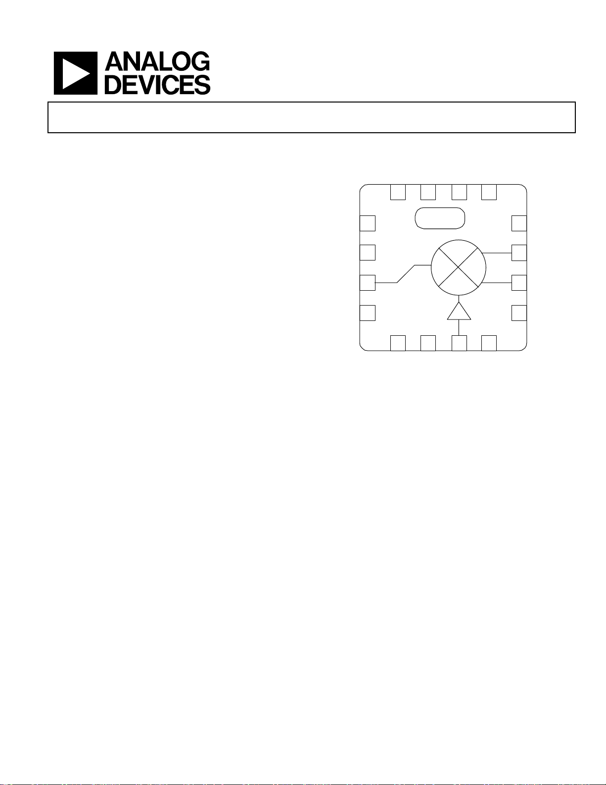
FUNCTIONAL BLOCK DIAGRAM
BPWDNVPDC
COMMEX
9101112
13
14
15
16
1234
VPLO LOCM LOIN COMM
BIAS
Figure 1.
AD8342
COMM
8
7
IFOP
IFOM
6
COMM
5
GENERAL DESCRIPTION
The AD8342 is a high performance, broadband active mixer. It
is well suited for demanding receive applications that require
wide bandwidth on all ports and very low intermodulation distortion and noise figure.
The AD8342 provides a typical conversion gain of 3dB at
500 MHz. The integrated LO driver supports a 50 Ω input impedance with a low LO drive level, helping to minimize external
component count.
The high input impedance RF port can be terminated and
driven single ended or a matching network can be used for best
noise or power match. The RF input accepts input signals as
large as 1.7 V p-p or 8 dBm (re: 50 Ω) at P
1dB
.
The open-collector differential outputs provide excellent balance and can be used with a differential filter or IF amplifier,
such as the AD8369 or AD8351. These outputs may also be
converted to a single-ended signal through the use of a matching network or a transformer (balun). When centered on the
VPOS supply voltage, each of the differential outputs may swing
2.5 V p-p.
The AD8342 is fabricated on an Analog Devices proprietary,
high performance SiGe IC process. The AD8342 is available in a
16-lead LFCSP package. It operates over a −40°C to +85°C temperature range. An evaluation board is also available.
Rev. PrB
Information furnished by Analog Devices is believed to be accurate and reliable. However, no
responsibility is assumed by Analog Devices for its use, nor for any infringements of patents
or other rights of third parties that may result from its use. Specifications subject to change
without notice. No license is granted by implication or otherwise under any patent or patent
rights of Analog Devices. Trademarks and registered trademarks are the property of their
respective owners.
One Technology Way, P.O. Box 9106, Norwood, MA 02062-9106, U.S.A.
Tel: 781.329.4700
Fax: 781.326.8703 © 2004 Analog Devices, Inc. All rights reserved.
www.analog.com
Page 2

AD8342 Preliminary Datasheet
SPECIFICATIONS
VS = 5 V, TA = 25°C, fRF = 500 MHz, fLO = 600 MHz, LO power = 0 dBm, ZO = 50 Ω, R
Table 1.
Parameter Conditions Min Typ Max Unit
RF INPUT INTERFACE (Pin 15, RFIN and Pin 14, RFCM)
Return Loss Hi-Z input terminated off-chip 10 dB
DC Bias Level Internally generated; port must be ac-coupled 2.5 V
OUTPUT INTERFACE
Output Impedance Differential impedance, f = 200 MHz 9||1 kΩ||pF
DC Bias Voltage Externally generated 4.75 VS 5.25 V
Power Range Via a 4:1 balun +13 dBm
LO INTERFACE
LO Power −10 0 +4 dBm
Return Loss 10 dB
DC Bias Voltage Internally generated; port must be ac-coupled VS − 1.6 V
POWER-DOWN INTERFACE
PWDN Threshold VS − 1.4 V
PWDN Response Time Device enabled, IF output to 90% of its final level 0.4 µs
Device disabled, supply current < 5 mA 0.01 µs
PWDN Input Bias Current Device enabled −80 µA
Device disabled +100 µA
POWER SUPPLY
Positive Supply Voltage 4.75 5 5.25 V
Quiescent Current
VPDC Supply current for bias cells 5 mA
VPMX, IFOP, IFOM Supply current for mixer, R
VPLO Supply current for LO limiting amplifier 35 mA
Total Quiescent Current VS = 5 V TBD 97 TBD mA
Power-Down Current Device disabled 500 µA
= 1.82 kΩ 57 mA
BIAS
= 1.82 kΩ, unless otherwise noted.
BIAS
Rev. PrB | Page 2 of 8
Page 3

Preliminary Datasheet AD8342
AC PERFORMANCE
VS = 5 V, TA = 25°C, LO power = 0 dBm, ZO = 50 Ω, R
Table 2.
Parameter Conditions Min Typ Max Unit
RF Frequency Range LF 500 MHz
LO Frequency Range High Side LO LF 850 MHz
IF Frequency Range Note: the upper “IF” is when used as an upconverter DC 350 MHz
Conversion Gain fRF = 460 MHz, fLO = 550 MHz, fIF = 90 MHz 3.2 dB
f
= 238 MHz, fLO = 286 MHz, fIF = 48 MHz 3.4 dB
RF
SSB Noise Figure fRF = 460 MHz, fLO = 550 MHz, fIF = 90 MHz 12.5 dB
f
Input Third-Order Intercept
Input Second-Order Intercept f
f
= 238 MHz, fLO = 286 MHz, fIF = 48 MHz 12.2 dB
RF
= 460 MHz, f
f
RF1
f
= 90 MHz, each RF tone -10 dBm
IF
= 238 MHz, f
f
RF1
= 45MHz, each RF tone -10 dBm
f
IF
= 460 MHz, f
RF1
= 238 MHz, f
RF1
Input 1 dB Compression Point fRF = 460 MHz, fLO = 550 MHz, fIF = 90 MHz 8.5 dBm
f
= 238 MHz, fLO = 286 MHz, fIF = 48 MHz 8.5 dBm
RF
LO to IF Output Leakage LO Power = 0 dBm, fRF = 500 MHz, fLO = 600 MHz TBD dBm
LO to RF Input Leakage LO Power = 0 dBm, fRF = 500 MHz, fLO = 600 MHz TBD dBm
2xLO to IF Output Leakage LO Power = 0 dBm, fRF = 500 MHz, fLO = 600 MHz TBD dBm
RF to IF Output Leakage RF Power = -10 dBm, fRF = 500 MHz, fLO = 600 MHz TBD dBm
IF/2 Spurious RF Power = -10 dBm, fRF = 500 MHz, fLO = 600 MHz TBD dBm
= 1.82 kΩ, unless otherwise noted.
BIAS
= 461 MHz, fLO = 550 MHz,
RF2
= 239 MHz, fLO = 286MHz,
RF2
= 480 MHz, fLO = 550 MHz, fIF = 90 MHz 48 dBm
RF2
= 248 MHz, fLO = 286 MHz, fIF = 48 MHz 48 dBm
RF2
22.5 dBm
23.5 dBm
Rev. PrB | Page 3 of 8
Page 4

AD8342 Preliminary Datasheet
ABSOLUTE MAXIMUM RATINGS
Table 3.
Parameter Rating
Supply Voltage, VS 5.5 V
RF Input Level 12 dBm
LO Input Level 12 dBm
PWDN Pin VS + 0.5 V
IFOP, IFOM Bias Voltage 5.5 V
Minimum Resistor from EXRB to COMM 1.82 kΩ
Internal Power Dissipation 580 mW
θJA 77°C/W
Maximum Junction Temperature 125°C
Operating Temperature Range −40°C to +85°C
Storage Temperature Range −65°C to +150°C
Lead Temperature Range (Soldering 60 sec) 300°C
ESD CAUTION
ESD (electrostatic discharge) sensitive device. Electrostatic charges as high as 4000 V readily accumulate
on the human body and test equipment and can discharge without detection. Although this product features
proprietary ESD protection circuitry, permanent damage may occur on devices subjected to high energy
electrostatic discharges. Therefore, proper ESD precautions are recommended to avoid performance
degradation or loss of functionality.
Stresses above those listed under Absolute Maximum Ratings
may cause permanent damage to the device. This is a stress
rating only; functional operation of the device at these or any
other conditions above those indicated in the operational section of this specification is not implied. Exposure to absolute
maximum rating conditions for extended periods may affect
device reliability.
Rev. PrB | Page 4 of 8
Page 5

Preliminary Datasheet AD8342
PIN CONFIGURATION AND FUNCTION DESCRIPTIONS
COMM
RFCM
RFIN
VPMX
VPDC12PWDN11EXRB10COMM
13
14
15
16
1
2
VPLO
LOCM
3
LOIN
9
4
COMM
8
7
6
5
COMM
IFOP
IFOM
COMM
04826-0-002
Figure 2. 16-Lead LFCSP
Table 4. Pin Function Descriptions
Pin No. Mnemonic Function
1 VPLO Positive Supply Voltage for the LO Buffer: 4.75 V to 5.25 V.
2 LOCM AC Ground for Limiting LO Amplifier, AC-Coupled to Ground.
3 LOIN LO Input. Nominal input level 0 dBm, input level range −10 dBm to +4 dBm, re: 50 Ω, ac-coupled.
4, 5, 8, 9, 13 COMM Device Common (DC Ground).
6, 7 IFOM, IFOP Differential IF Outputs; Open Collectors, Each Requires DC Bias of 5.00 V (Nominal).
10 EXRB
Mixer Bias Voltage, Connect Resistor from EXRB to Ground, Typical Value of 1.82 kΩ
Sets Mixer Current to Nominal Value. Minimum resistor value from EXRB to ground = 1.82 kΩ.
11 PWDN Connect to Ground for Normal Operation. Connect pin to VS for disable mode.
12 VPDC Positive Supply Voltage for the DC Bias Cell: 4.75 V to 5.25 V.
14 RFCM AC Ground for RF Input, AC-Coupled to Ground.
15 RFIN RF Input. Must be ac-coupled.
16 VPMX Positive Supply Voltage for the Mixer: 4.75 V to 5.25 V.
Rev. PrB | Page 5 of 8
Page 6

AD8342 Preliminary Datasheet
p
5
4.5
4
3.5
3
2.5
2
Conversion Gain - dB
1.5
1
0.5
0
100 150 200 250 300 350 400 450 500
10MHz
RF Frequency - MHz
48MHz
90MHz
140MHz
Figure 3. Conversion Gain vs. RF Frequency for Multiple IF Frequencies
12
11
10
9
8
ut P1dB - dB m
In
7
6
5
100 150 200 250 300 350 400 450 500
10MHz
RF Frequency - MHz
48MHz
90MHz
140MHz
Figure 5. Input Compression Point vs RF Frequency for Multiple IF Frequencies
15
14
13
12
11
10
NF - dB
9
8
7
6
5
100 150 200 250 300 350 400 450 500
10MHz
RF Frequency - MHz
90MHz
48MHz
140MHz
Figure 4. Single Sideband Noise Figure vs RF Frequency for Multiple IF
Freque ncies
30
25
20
15
IIP 3 - d B m
10
5
0
100 150 200 250 300 350 400 450 500
Figure 6.. Input IP3 vs. RF Frequency for Multiple IF Frequencies
10MHz
RF Frequency - MHz
48MHz
90MHz
140MHz
Rev. PrB | Page 6 of 8
Page 7

Preliminary Datasheet AD8342
EVALUATION BOARD
An evaluation board is available for the AD8342. The evaluation board is configured for single-ended signaling at the IF output port via a
balun transformer. The schematic for the evaluation board is presented in Figure 7.
Figure 7. Customer Evaluation Board
Table 5. Evaluation Boards Configuration Options
Component Function Default Conditions
R1, R2, R7,
C2, C4, C5, C6,
C12, C13, C14,
C15
R3, R4, R15, R16
R6, C11
C3, R14, C16, L1
C1
C8
C7
SW1
R8, R9
T1,
R10, R11, R12,
Z1, Z2, Z3, Z4
Supply Decoupling.
Power supply decoupling resistors and filter capacitors.
Jumpers for IF output interface. The eval board can be configured to provide a
balanced differential output by removing R15 and T1 and adding 0-Ω resistors for
R3, R4, and R16 and adding suitable choke inductors for Z1 and Z3.
resistor that sets the bias current for the mixer core.
R
BIAS
The capacitor provides ac bypass for R6.
RF Input. C3 Provides dc block for RF input. R14 provides a resistive input
termination. C16 and L1 are provided for reactive matching the input.
RF Common AC Coupling. Provides dc block for RF input common connection.
LO Input AC Coupling. Provides dc block for the LO input.
LO Common AC Coupling. Provides dc block for LO input common connection.
Power Down. The part is on when the PWDN is connected to a low potential. The
part is disabled when PWDN is connected to the positive supply via SW1. R8
provides a pull-down when SW1 is open and can be used as a termination when
excercising the PWDN feature with an external generator.
IF Output Interface. R12 Provides a real 100 -Ω termination to the open collector
outputs. T1 converts differential, high impedance IF output to single-ended. The
center tap of the primary is used to supply the bias voltage (V
pins.
) to the IF output
S
R1, R2, R7 = 0 Ω (Size 0603)
C4, C6, C13, C14 = 100 pF
(Size 0603)
C2, C5, C12, C15 = 0.1 µF
(Size 0603)
R3=R4=R16=open
R15=0 Ω (Size 0402)
R6 = 1.82 kΩ (Size 0603)
C11 = 100 pF (Size 0603)
C3 = 1000 pF (Size 0402)
R14 = 100 Ω (Size 0603)
C16 = open (Size 0603)
L1 = 0 Ω (Size 0603)
C1 = 1000 pF (Size 0402)
C8 = 100 pF (Size 0402)
C7 = 100 pF (Size 0402)
R8 = 10 kΩ (Size 0603)
R9 = 0 Ω (Size 0603)
T1 = TC2-1T, 2:1 (Mini-Circuits)
R10=R11 = 0 Ω (Size 0603) R12 =
100 Ω (Size 0603)
Z1 = Z2 = Open
Z3 = Z4 = Open
Rev. PrB | Page 7 of 8
Page 8

AD8342 Preliminary Datasheet
PR05352-0-1/05(PrB)
OUTLINE DIMENSIONS
0.50
0.40
PIN 1
INDICATOR
1.00
0.85
0.80
SEATING
PLANE
12° MAX
3.00
BSC SQ
TOP VIEW
0.30
0.23
0.18
2.75
BSC SQ
0.80 MAX
0.65 TYP
0.05 MAX
0.02 NOM
0.20 REF
*
COMPLIANTTO JEDEC STANDARDS MO-220-VEED-2
EXCEPT FOR EXPOSED PAD DIMENSION
0.45
0.50
BSC
1.50 REF
0.60 MAX
Figure 7. 16-Lead Lead Frame Chip Scale Package [LFCSP]
3 mm × 3 mm Body (CP-16-3)
Dimensions in millimeters
13
12
9
8
BOTTOM
VIEW
0.30
16
1
4
5
PIN 1 INDICATOR
1.65
*
1.50 SQ
1.35
0.25 MIN
© 2004 Analog Devices, Inc. All rights reserved. Trademarks and registered trademarks are the property of their respective owners.
Rev. PrB | Page 8 of 8
 Loading...