

Page 1
5 V CATV Line Driver Coarse Step
FUNDAMENTAL FREQUENCY – MHz
–50
–60
–75
–65
–55
5 152535455565
DISTORTION – dBc
–70
HD3
HD2
V
OUT
= 60dBmV @ MAX GAIN
a
FEATURES
Supports DOCSIS Standard for Reverse Path
Transmission
Gain Programmable in 6.02 dB Steps over a 48.16 dB
Range
Low Distortion at 60 dBmV Output
–63 dBc SFDR at 21 MHz
–57 dBc SFDR at 42 MHz
Output Noise Level
–47 dBmV in 160 kHz
Maintains 75 ⍀ Output Impedance
Transmit Enable and Transmit Disable Modes
Upper Bandwidth: 160 MHz (Full Gain Range)
5 V Supply Operation
Supports SPI Interfaces
APPLICATIONS
Gain-Programmable Line Driver
DOCSIS High-Speed Data Modems
Interactive Cable Set-Top Boxes
PC Plug-in Cable Modems
General-Purpose Digitally Controlled Variable Gain Block
V
IN+
V
IN–
ZIN (SINGLE) = 800⍀
Z
(DIFF) = 1.6k⍀
IN
Output Power Control
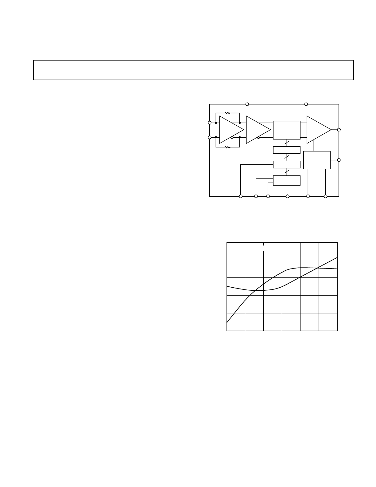
FUNCTIONAL BLOCK DIAGRAM
VCC (5 PINS)
R1
DIFF OR
SINGLE
INPUT
AMP
R2
VERNIER
DATA CLK GND (5 PINS)
DATEN
ATTENUATION
CORE
8
DECODE
8
DATA LATCH
8
SHIFT
REGISTER
AD8327
BYP
AD8327
POWER
AMP
= 75⍀
Z
OUT
POWER-DOWN
LOGIC
TXEN
SLEEP
V
OUT
CXR
GENERAL DESCRIPTION
The AD8327 is a low-cost, digitally controlled, variable gain
amplifier optimized for coaxial line driving applications such as
cable modems that are designed to the MCNS-DOCSIS
upstream standard. An 8-bit serial word determines the desired
output gain over a 48.16 dB range resulting in gain changes of
6.02 dB/major carry.
The AD8327 comprises a digitally controlled variable attenuator
of 0 dB to –48.16 dB, which is preceded by a low noise, fixed
gain buffer and followed by a low distortion, high power amplifier.
The AD8327 accepts a differential or single-ended input
signal. The output is specified for driving a 75 Ω load, such
as coaxial cable.
Distortion performance of –63 dBc is achieved with an output
level up to 60 dBmV at 21 MHz bandwidth. A key performance
and cost advantage of the AD8327 results from the ability to
maintain a constant 75 Ω output impedance during Transmit
Enable and Transmit Disable conditions. In addition, this
device has a sleep mode function that reduces the quiescent
current to 5 mA.
The AD8327 is packaged in a low-cost 20-lead TSSOP, operates
from a single 5 V supply, and has an operational temperature
range of –40°C to +85°C.
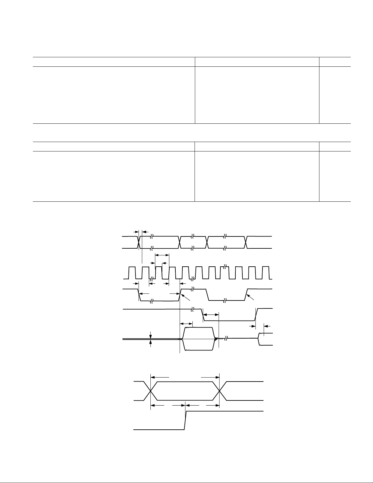
Figure 1. Harmonic Distortion vs. Frequency
REV. 0
Information furnished by Analog Devices is believed to be accurate and
reliable. However, no responsibility is assumed by Analog Devices for its
use, nor for any infringements of patents or other rights of third parties that
may result from its use. No license is granted by implication or otherwise
under any patent or patent rights of Analog Devices.
One Technology Way, P.O. Box 9106, Norwood, MA 02062-9106, U.S.A.
Tel: 781/329-4700 www.analog.com
Fax: 781/326-8703 © Analog Devices, Inc., 2001
Page 2

AD8327–SPECIFICATIONS
(TA = 25ⴗC, VS = 5 V, RL = 75 ⍀, V
IN(DIFFERENTIAL)
= 30 dBmV)
Parameter Conditions Min Typ Max Unit
INPUT CHARACTERISTICS
Specified AC Voltage P
= 60 dBmV, Max Gain 30 dBmV
OUT
Noise Figure Max Gain, f = 10 MHz 13.2 dB
Input Resistance Single-Ended Input 800 Ω
Differential Input 1600 Ω
Input Capacitance 2pF
GAIN CONTROL INTERFACE
Gain Range 47.16 48.16 49.16 dB
Maximum Gain Gain Code = 10000000 (128 Decimal) 29 30 31 dB
Minimum Gain Gain Code = 00000000 (0 Decimal) –19.16 –18.16 –17.16 dB
Gain Scaling Factor 6.02 dB/Major
Carry
OUTPUT CHARACTERISTICS
Bandwidth (–3 dB) All Gain Codes 160 MHz
Bandwidth Roll-Off f = 65 MHz 0.4 dB
Bandwidth Peaking All Gain Codes 0 dB
Output Noise Spectral Density Max Gain, f = 10 MHz –32 dBmV in
160 kHz
Min Gain, f = 10 MHz –47 dBmV in
160 kHz
Transmit Disable Mode (TXEN = 0), –66 dBmV in
f = 10 MHz 160 kHz
1 dB Compression Point Max Gain, f = 10 MHz 14.8 dBm
Differential Output Impedance Transmit Enable (TXEN = 1) and
Transmit Disable Mode (TXEN = 0) 75 ± 20% Ω
OVERALL PERFORMANCE
Second Order Harmonic Distortion f = 21 MHz, V
f = 42 MHz, V
f = 65 MHz, V
Third Order Harmonic Distortion f = 21 MHz, V
f = 42 MHz, V
f = 65 MHz, V
= 60 dBmV @ Max Gain –63 dBc
OUT
= 60 dBmV @ Max Gain –61 dBc
OUT
= 60 dBmV @ Max Gain –54 dBc
OUT
= 60 dBmV @ Max Gain –63 dBc
OUT
= 60 dBmV @ Max Gain –57 dBc
OUT
= 60 dBmV @ Max Gain –57 dBc
OUT
Adjacent Channel Power Adjacent Channel Width = Transmit Channel –62 dBc
Width = 160 K
SYM/SEC
Gain Linearity Error f = 10 MHz, Code to Code ±0.25 dB
Output Settling
Due to Gain Change (T
Due to Input Change Max Gain, V
) Min to Max Gain 60 ns
GS
= 30 dBmV 30 ns
IN
Isolation in Transmit Disable Mode Max Gain, TXEN = 0 V, f = 42 MHz, –52 dBc
VIN = 30 dBmV
POWER CONTROL
Transmit Enable Settling Time (T
Transmit Disable Settling Time (T
Transmit Enable Settling Time (T
Transmit Disable Settling Time (T
Between Burst Transients
Ramp Setting
2
2
)1Max Gain, VIN = 0 V 300 ns
ON
)1Max Gain, VIN = 0 V 40 ns
OFF
)2Max Gain, VIN = 0 V 2 µs
ON
)2Max Gain, VIN = 0 V 1.7 µs
OFF
Equivalent Output = 31 dBmV 3 mV p-p
Equivalent Output = 60 dBmV 25 mV p-p
2 µs
POWER SUPPLY
Operating Range 4.75 5 5.25 V
Quiescent Current Transmit Enable Mode (TXEN = 1) @ Dec 128 75 105 135 mA
Transmit Enable Mode (TXEN = 1) @ Dec 0 40 60 80 mA
Transmit Disable Mode @ All Gain Codes 10 15 20 mA
Sleep Mode @ All Gain Codes 3 5 7 mA
OPERATING TEMPERATURE –40 +85 °C
RANGE
NOTES
1
For Transmit Enable or Transmit Disable transitions using a 0 pF capacitor (at CXR pin) to ground.
2
For Transmit Enable or Transmit Disable transitions using a 100 pF capacitor (at CXR pin) to ground.
Specifications subject to change without notice.
–2–
REV. 0
Page 3
AD8327
LOGIC INPUTS (TTL/CMOS-Compatible Logic)
(DATEN, CLK, SDATA, TXEN, SLEEP, VCC = 5 V: Full Temperature Range)
Parameter Min Typ Max Unit
Logic “1” Voltage 2.1 5.0 V
Logic “0” Voltage 0 0.8 V
Logic “1” Current (V
Logic “0” Current (V
Logic “1” Current (V
Logic “0” Current (V
Logic “1” Current (V
Logic “0” Current (V
TIMING REQUIREMENTS
= 5 V) CLK, SDATA, DATEN 020nA
INH
= 0 V) CLK, SDATA, DATEN –600 –100 nA
INL
= 5 V) TXEN 50 190 µA
INH
= 0 V) TXEN –250 –30 µA
INL
= 5 V) SLEEP 50 190 µA
INH
= 0 V) SLEEP –250 –30 µA
INL
(Full Temperature Range, VCC = 5 V, tR = tF = 4 ns, f
= 8 MHz unless otherwise noted.)
CLK
Parameter Min Typ Max Unit
Clock Pulsewidth (t
Clock Period (t
Setup Time SDATA vs. Clock (t
Setup Time DATEN vs. Clock (t
Hold Time SDATA vs. Clock (t
Hold Time DATEN vs. Clock (t
) 16.0 ns
WH
) 32.0 ns
C
) 5.0 ns
DS
) 15.0 ns
ES
) 5.0 ns
DH
) 3.0 ns
EH
Input Rise and Fall Times, SDATA, DATEN, Clock (tR, tF)10ns
t
DS
SDATA
CLK
DATEN
TXEN
ANALOG
OUTPUT
VALID DATA WORD G1
MSB. . . .LSB
t
ES
8 CLOCK
CYCLES
SIGNAL AMPLITUDE (p-p)
Figure 2. Serial Interface Timing
SDATA
MSB MSB-1
t
C
t
WH
t
EH
GAIN TRANSFER (G1)
t
GS
VALID DATA BIT
t
DS
VALID DATA WORD G2
t
OFF
t
DH
GAIN TRANSFER (G2)
t
MSB-2
ON
REV. 0
CLK
Figure 3. SDATA Timing
–3–
Page 4
AD8327
TOP VIEW
(Not to Scale)
20
19
18
17
16
15
14
13
12
11
1
2
3
4
5
6
7
8
9
10
AD8327
DATEN
V
IN–
V
IN+
GND
V
CC
SLEEP
BYP
V
CC
V
CC
GND
SDATA
CLK
GND
V
CC
TXEN
V
CC
V
OUT
GND
GND
CXR
WARNING!
ESD SENSITIVE DEVICE
ABSOLUTE MAXIMUM RATINGS*
Supply Voltage +V
S
PIN CONFIGURATION
Pins 4, 6, 11, 12, 16 . . . . . . . . . . . . . . . . . . . . . . . . . . . . 6 V
Input Voltages
Pins 17, 18 . . . . . . . . . . . . . . . . . . . . . . . . . . . . . . . . ±0.5 V
Pins 1, 2, 3, 19, 20 . . . . . . . . . . . . . . . . . . . –0.8 V to +5.5 V
Internal Power Dissipation
TSSOP . . . . . . . . . . . . . . . . . . . . . . . . . . . . . . . . . 810 mW
Operating Temperature Range . . . . . . . . . . . –40°C to +85°C
Storage Temperature Range . . . . . . . . . . . . –65°C to +150°C
Lead Temperature, Soldering 60 seconds . . . . . . . . . . . 300°C
*Stresses above those listed under Absolute Maximum Ratings may cause perma-
nent damage to the device. This is a stress rating only; functional operation of the
device at these or any other conditions above those indicated in the operational
section of this specification is not implied. Exposure to absolute maximum rating
conditions for extended periods may affect device reliability.
PIN FUNCTION DESCRIPTIONS
Pin No. Mnemonic Description
1 SDATA Serial Data Input. This digital input allows for an 8-bit serial (gain) word to be loaded into the
internal register with the MSB (Most Significant Bit) first.
2 CLK Clock Input. The clock port controls the serial attenuator data transfer rate to the 8-bit master-
slave register. A Logic 0-to-1 transition latches the data bit and a 1-to-0 transfers the data bit to
the slave. This requires the input serial data word to be valid at or before this clock transition.
3 TXEN Logic “0” disables transmission. Logic “1” enables transmission.
4, 6, 11, 12, 16 V
CC
Common Positive External Supply Voltage. A 0.1 µF capacitor must decouple each pin.
5, 8, 9, 13, 15 GND Common External Ground Reference
7 CXR Transmit Enable/Disable Timing Capacitor. This pin is decoupled with a 100 pF capacitor to GND.
10 V
OUT
Output Signal
14 BYP Internal Bypass. This pin must be externally ac-coupled (0.1 µF capacitor).
17 V
IN+
Noninverting Input. DC-biased to approximately VCC/2. Should be ac-coupled with a 0.1 µF
capacitor.
18 V
IN–
19 SLEEP Low Power Sleep Mode. Logic 0 enables Sleep mode, where Z
Inverting Input. DC-biased to approximately VCC/2. Should be ac-coupled with a 0.1 µF capacitor.
goes to 200 Ω and supply
OUT
current is reduced to 5 mA. Logic 1 enables normal operation.
20 DATEN Data Enable Low Input. This port controls the 8-bit parallel data latch and shift register. A Logic
0-to-1 transition transfers the latched data to the attenuator core (updates the gain) and simultaneously inhibits serial data transfer into the register. A 1-to-0 transition inhibits the data latch
(holds the previous gain state) and simultaneously enables the register for serial data load.
ORDERING GUIDE
Model Temperature Range Package Description
JA
Package Option
AD8327ARU –40°C to +85°C 20-Lead TSSOP 85°C/W* RU-20
AD8327ARU-REEL –40°C to +85°C 20-Lead TSSOP 85°C/W* RU-20
AD8327-EVAL Evaluation Board
*Thermal Resistance measured on SEMI standard 4-layer board.
CAUTION
ESD (electrostatic discharge) sensitive device. Electrostatic charges as high as 4000 V readily
accumulate on the human body and test equipment and can discharge without detection. Although
the AD8327 features proprietary ESD protection circuitry, permanent damage may occur on
devices subjected to high-energy electrostatic discharges. Therefore, proper ESD precautions are
recommended to avoid performance degradation or loss of functionality.
–4–
REV. 0
Page 5
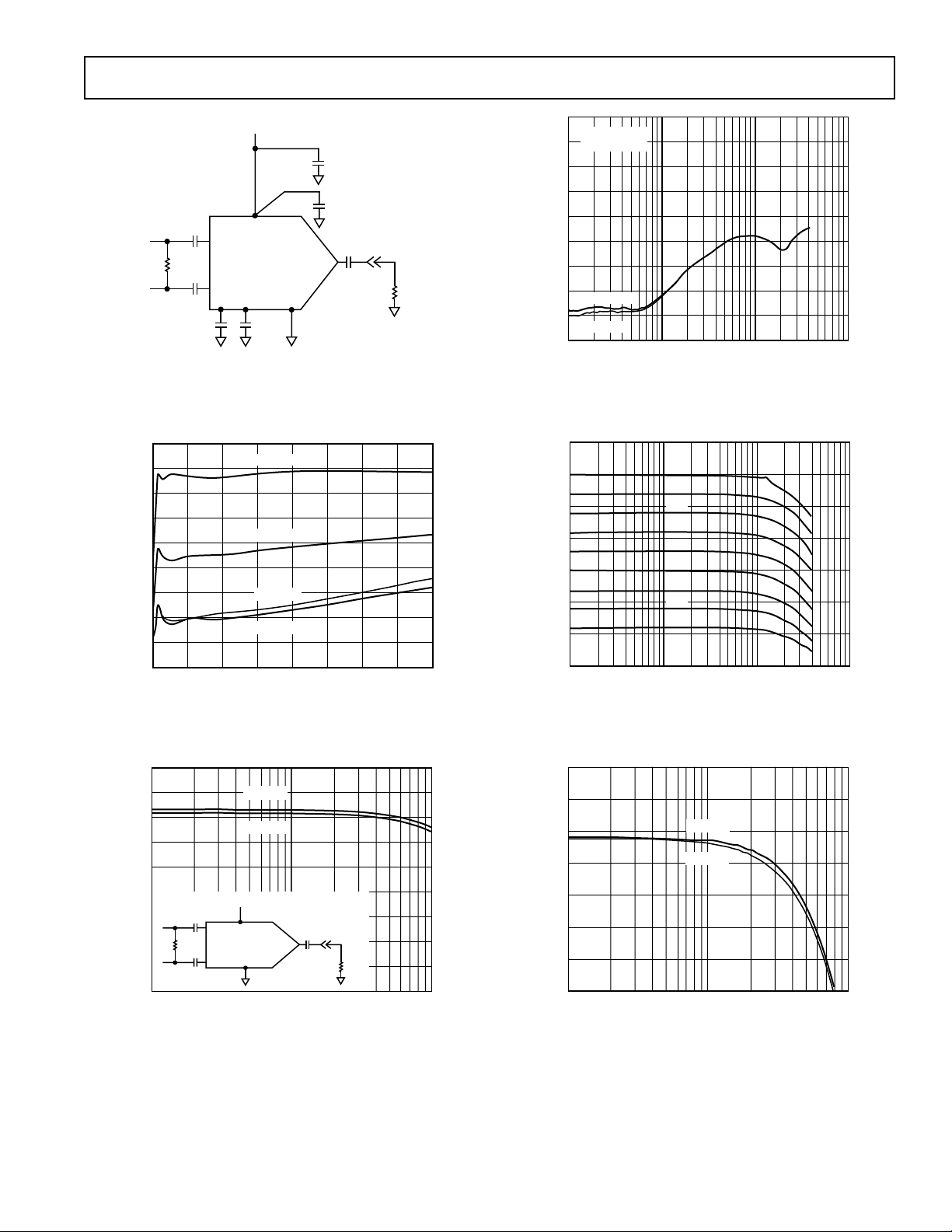
Typical Performance Characteristics–AD8327
FREQUENCY – MHz
0
–10
–90
1
100010
ISOLATION – dBc
100
–20
–30
–70
–40
–50
–60
–80
TXEN = 0
VIN = 30dBmV
MAX GAIN
MIN GAIN
FREQUENCY – MHz
100
10
1000
1
10
–20
–30
0
–10
20
30
40
GAIN – dB
128D
64D
32D
01D
16D
08D
04D
02D
00D
FREQUENCY – MHz
90
85
80
75
70
65
60
55
1
100
10
IMPEDANCE – ⍀
TXEN = 0
TXEN = 1
+V
S
10F
0.1F
0.1F
V
165⍀
IN
0.1F
0.1F
V
IN–
AD8327
V
IN+
BYP CXR
V
CC
100pF
GND
0.1F
75⍀
REV. 0
TPC 1. Basic Test Circuit
0.6
0.5
0.4
0.3
0.2
0.1
0
GAIN ERROR – dB
–0.1
–0.2
–0.3
0 16 48 80 96 112 12832 64
f = 65MHz
f = 42MHz
f = 10MHz
f = 5MHz
GAIN CONTROL – Decimal Code
TPC 2. Gain Error vs. Gain Control
160
155
150
145
140
135
IMPEDANCE – ⍀
130
125
120
115
0.1F
165⍀
V
IN
0.1F
1
TPC 3. Input Impedance vs. Frequency
TXEN = 0
TXEN = 1
+V
S
V
IN–
AD8327
V
GND
IN+
FREQUENCY – MHz
OUT
0.1F
75⍀
10
TPC 4. Isolation in Transmit Disable Mode
vs. Frequency
TPC 5. AC Response
100
TPC 6. Output Impedance vs. Frequency
–5–
Page 6
AD8327
–50
V
= 61dBmV
–55
–60
DISTORTION – dBc
–65
–70
56515
V
= 60dBmV
OUT
@ MAX GAIN
25 35 45 55
FUNDAMENTAL FREQUENCY – MHz
OUT
@ MAX GAIN
V
= 58dBmV
OUT
@ MAX GAIN
V
= 59dBmV
OUT
@ MAX GAIN
TPC 7. Second Order Harmonic Distortion vs. Frequency
for Various Output Levels
–50
FO = 5MHz
= 60dBmV @ MAX GAIN
V
–55
OUT
–60
–65
–70
–75
DISTORTION – dBc
–80
–85
HD2
HD3
–50
V
–55
–60
–65
–70
DISTORTION – dBc
–75
–80
= 61dBmV @ MAX GAIN
OUT
V
OUT
535
25 4515
FUNDAMENTAL FREQUENCY – MHz
V
= 60dBmV @ MAX GAIN
OUT
V
= 59dBmV @ MAX GAIN
OUT
= 58dBmV @ MAX GAIN
55 65
TPC 10. Third Order Harmonic Distortion vs. Frequency
for Various Output Levels
–50
FO = 21MHz
= 60dBmV @ MAX GAIN
V
OUT
–55
–60
–65
–70
–75
DISTORTION – dBc
–80
–85
HD2
HD3
–90
0 12816
32 48 64 112
GAIN CONTROL – Decimal Code
80 96
TPC 8. Harmonic Distortion vs. Gain Control
–50
F
= 42MHz
O
–55
–60
–65
–70
–75
DISTORTION – dBc
–80
–85
–90
= 60dBmV @ MAX GAIN
V
OUT
04832 6416
HD2
HD3
80 96
GAIN CONTROL – Decimal Code
112 128
TPC 9. Harmonic Distortion vs. Gain Control
–90
0 12816
32 48 64 112
GAIN CONTROL – Decimal Code
80 96
TPC 11. Harmonic Distortion vs. Gain Control
–50
FO = 65MHz
= 60dBmV @ MAX GAIN
V
OUT
–55
–60
–65
–70
–75
DISTORTION – dBc
–80
–85
–90
0 12816
32 48 64 112
GAIN CONTROL – Decimal Code
HD2
HD3
80 96
TPC 12. Harmonic Distortion vs. Gain Control
–6–
REV. 0
Page 7

AD8327
–10
–20
CH PWR 9.0dBm
ACP UP –62dBc
ACP LOW –62.5dBc
–30
–40
–50
–60
–70
–80
–90
–100
–110
C11
CENTER 21MHz 75kHz/DIV SPAN 750kHz
C11
C0
Cu1
C0
Cu1
TPC 13. Adjacent Channel Power
–30
f = 10MHz
TXEN = 1
–34
–38
–42
–46
OUTPUT NOISE – dBmV in 160kHz
–50
0 12816 32 48 64 80 96 112
GAIN CONTROL – Decimal Code
TPC 14. Output Referred Noise vs. Gain Control
60
V
= 60dBmV
OUT
50
@ MAX GAIN
40
30
20
10
0
– dBmV
OUT
–10
V
–20
–30
–40
41.0 43.041.2 41.4 41.8 42.0 42.2 42.4 42.6 42.841.6
FREQUENCY – MHz
TPC 16. Two-Tone Intermodulation Distortion
–25
–30
@ MAX GAIN, TXEN = 1
–35
–40
–45
@ MIN GAIN, TXEN = 1
–50
–55
–60
–65
OUTPUT NOISE – dBmV in 160kHz
ALL GAIN CODES, TXEN = 0
–70
–75
56515 25 35 45 55
FREQUENCY – MHz
TPC 17. Output Referred Noise vs. Frequency for Various
Gain Codes
35
V
= 60dBmV
GAIN – dB
30
25
20
15
10
1
OUT
@ MAX GAIN
0.1F
V
V
165⍀
IN
V
BYP
0.1F
0.1F
IN–
IN+
V
AD8327
CXR
CC
100pF
+V
S
GND
10F
0.1F
0.1F
CL = 20pF
C
L
CL = 50pF
C
= 0pF
L
CL = 10pF
75⍀
100
FREQUENCY – MHz
TPC 15. AC Response for Various Capacitor Loads
REV. 0
120
TXEN = 1
110
100
90
80
70
60
QUIESCENT SUPPLY CURRENT – mA
100010
50
0 12816 32 48 64 80 96 112
GAIN CONTROL – Decimal Code
TPC 18. Supply Current vs. Gain Code
–7–
Page 8

AD8327
APPLICATIONS
General Application
The AD8327 is primarily intended for use as the upstream power
amplifier (PA), also known as a line driver, in DOCSIS (Data
Over Cable Service Interface Specification) certified cable
modems and CATV set-top boxes. The upstream signal is either
a QPSK or QAM signal generated by a DSP, a dedicated QPSK/
QAM modulator, or a DAC.
In all cases the signal must be low-pass filtered before being
applied to the PA in order to filter out-of-band noise and higher
order harmonics from the amplified signal. Due to the varying
distances between the cable modem and the headend, the
upstream PA must be capable of varying the output power by
applying gain or attenuation. The varying output power of the
AD8327 ensures that the signal from the cable modem will have
the proper level once it arrives at the headend. The upstream
signal path commonly includes a diplexer and cable splitters.
The AD8327 has been designed to overcome losses associated
with these passive components in the upstream cable path.
Circuit Description
The AD8327 is composed of three analog functions in the powerup or forward mode. The input amplifier (preamp) can be used
single-ended or differentially. If the input is used in the differential configuration, it is imperative that the input signals be 180
degrees out of phase and of equal amplitude. The preamp stage
drives a DAC, which provides the AD8327’s attenuation (eight
bits or 48.16 dB). The signals in the preamp and DAC gain
blocks are differential to improve the PSRR and linearity.
A differential current is fed from the DAC into the output stage,
which amplifies these currents to the appropriate levels necessary to
drive a 75 Ω load. The output stage maintains 75 Ω output
impedance, eliminating the need for external matching resistors.
SPI Programming and Gain Adjustment
The AD8327 is controlled through a serial peripheral interface
(SPI) of three digital data lines: CLK, DATEN, and SDATA.
Changing the gain requires eight bits of data to be streamed into
the SDATA port. The sequence of loading the SDATA register
begins on the falling edge of the DATEN pin, which activates
the CLK line. With the CLK line activated, data on the SDATA
line is clocked into the serial shift register, Most Significant Bit
(MSB) first, on the rising edge of the CLK pulses. The 8-bit
data word is latched into the attenuator core on the rising edge
of the DATEN line. This provides control over the changes in
the output signal level. The serial interface timing for the AD8327
is shown in Figures 2 and 3. The programmable gain range of
the AD8327 is –18.16 dB to +30 dB with steps of 6.02 dB per
major carry. This provides a total gain range of 48.16 dB.
The AD8327 was characterized with a TOKO transformer
(TOKO#617DB-A0070) on the input, and the stated gain
values account for the losses due to the transformer. Table I
shows the possible gain states.
Input Bias, Impedance, and Termination
The V
IN+
and V
inputs have a dc bias level of VCC/2, therefore
IN–
the input signal should be ac-coupled using 0.1 µF capacitors as
seen in the typical application circuit (see Figure 4). The differential input impedance of the AD8327 is approximately 1.6 kΩ,
while the single-ended input impedance is 800 Ω.
Table I. Gain States
Decimal Code Bit 7 Bit 6 Bit 5 Bit 4 Bit 3 Bit 2 Bit 1 Bit 0 Gain
0 00000000–18.16
1 00000001–12.14
2 00000010–6.12
4 00000100–0.10
8 000010005.92
16 0001000011.94
32 0010000017.96
64 0100000023.98
128 1000000030
–8–
REV. 0
Page 9

Z
1600⍀
Z
1600⍀
V
CC
SLEEP
ENB
SDATA
CLK
TXEN
10F
0.1F
0.1F
100pF
AD8327
1
SDATA
2
CLK
3
TXEN
4
V
CC
5
GND
6
V
CC
7
CXR
8
GND
9
GND
10
V
OUT
0.1F
TO DIPLEXER ZIN = 75⍀
SLEEP
ENB
V
V
V
GND
BYP
GND
V
V
IN–
IN+
CC
CC
CC
Figure 4. Typical Application Circuit
Single-Ended Inverting Input
When operating the AD8327 in a single-ended input mode V
and V
should be terminated as illustrated in Figure 5. On the
IN–
IN+
AD8327 evaluation boards, this termination method requires
the removal of R13–R16 and R20, as well as the addition of a 0 Ω
jumper at R17. Table II shows the correct values for R11 and R12
for some common input configurations. Other input impedance configurations may be accommodated using the equations
in Figure 5. The inverting and noninverting inputs of the AD8327
must be balanced for all input configurations
Z
ⴛ 800⍀
IN
R12 =
800⍀
– ZIN
R12
Z
IN
R11
R11 =
ZIN ⴛ R12
R12
+ ZIN
–
AD8327
+
Figure 5. Single-Ended Inverting Input
Differential Input from Single-Ended Source
The default configuration of the evaluation board implements a
differential signal drive from a single-ended signal source. A
TOKO 1:1 transformer is included on the board for this purpose
(T3). Enabling the evaluation board for single to differential input
conversion requires R11–R12 and R16–R17 to be removed, and
0 Ω jumpers must be installed on the placeholders for R14, R15,
and R20. Table II provides typical R13 values for common
input configurations. Other input impedances may be calculated
using the equation in Figure 6. Refer to Figure 10 for evaluation
board schematic. To utilize the transformer for converting a singleended source into a differential signal, the input signal must
be applied to V
IN+
.
AD8327
20
19
18
17
16
15
14
13
12
11
Z
IN
Figure 6. Single to Differential Input
Differential Signal Source
The AD8327 evaluation board is also capable of accepting a
differential input signal. Remove R11–R12, R14–R15, and R20,
and place 0 Ω jumpers for R16–R17. See Table II for common
values of R13, or calculate other input configurations using the
equation in Figure 7.
Z
IN
Output Bias, Impedance, and Termination
The output of the AD8327 has a dc bias level of approximately
V
/2; therefore, it should be ac-coupled before being applied to
CC
the load. The output impedance of the AD8327 is internally
maintained at 75 Ω, regardless of whether the amplifier is in
transmit enable or transmit disable mode. This eliminates the
need for external back termination resistors. If the output signal
is being evaluated using standard 50 Ω test equipment, a minimum loss 75 Ω to 50 Ω pad must be used to provide the test
circuit with the proper impedance match.
0.1F
165⍀
0.1F
0.1F
0.1F
0.1F
0.1F
ⴛ
IN
R13 =
1600⍀ – Z
+
V
IN
R13 =
VIN+
VIN–
ⴛ
IN
1600⍀ – Z
R13
IN
R13
Figure 7. Differential Input
V
IN–
ZIN = 150⍀
V
IN+
IN
AD8327
AD8327
REV. 0
–9–
Page 10

AD8327
Table II. Common Input Terminations
Differential Input Termination
ZIN (⍀) R11 R12 R13 (⍀)
50 Open Open 52.1
75 Open Open 78.7
100 Open Open 107
150 Open Open 165
Single-Ended Input Termination
ZIN (⍀) R11 (⍀) R12 (⍀) R13
50 25.5 53.6 Open
75 39.2 82.5 Open
Power Supply
The 5 V supply should be delivered to each of the VCC pins via a
low impedance power bus to ensure that each pin is at the same
potential. The power bus should be decoupled to ground using
a 10 µF tantalum capacitor located close to the AD8327ARU.
In addition to the 10 µF capacitor, each V
vidually decoupled to ground with 0.1 µF ceramic chip capaci-
indi
tors
located close to the pins. The bypass pin, labeled BYP (Pin 14),
pin should be
CC
should also be decoupled with a 0.1 µF capacitor. The PCB
should have a low impedance ground plane covering all unused
portions of the board, except in areas of the board where input
and output traces are in close proximity to the AD8327. All
AD8327 ground pins must be connected to the ground plane to
ensure proper grounding of all internal nodes.
CXR Pin
The AD8327 features internal circuitry that controls burst
transients. This feature uses a 100 pF capacitor connected to
Pin 7 of the AD8327, to slow down the turn-on transient and
minimize between-burst transients.
Signal Integrity Layout Considerations
Careful attention to printed circuit board layout details will
prevent problems due to board parasitics. Proper RF design
techniques are mandatory. The differential input and output
traces should be kept as short as possible. It is also critical that
all differential signal paths be symmetrical in length and width.
In addition, the input and output traces should be kept far apart,
to minimize coupling (crosstalk) through the board. Following
these guidelines will optimize the overall performance of the
AD8327 in all applications.
Initial Power-Up
When the supply voltage is first applied to the AD8327, the gain
of the amplifier is initially set to gain code 0. As power is first
applied to the amplifier, the TXEN pin should be held low
(Logic 0) to prevent forward signal transmission. After power
has been applied to the amplifier, the gain can be set to the
desired level by following the procedure provided in the SPI
Programming and Gain Adjustment section. The TXEN pin
can then be brought from Logic 0 to Logic 1, enabling forward
signal transmission at the desired gain level.
Asynchronous Power-Down
The asynchronous TXEN pin is used to place the AD8327 into
between-burst mode, while maintaining a differential output
impedance of 75 Ω. Applying Logic 0 to the TXEN pin activates
the on-chip reverse amplifier, providing an 86% reduction in
consumed power. For 5 V operation, the supply current is typically
reduced from 105 mA to 15 mA. In this mode of operation,
between-burst noise is minimized and the amplifier can no longer
transmit in the upstream direction. In addition to the TXEN
pin, the AD8327 also incorporates an asynchronous SLEEP pin,
which may be used to further reduce the supply current to
approximately 5 mA. Applying Logic 0 to the SLEEP pin places
the amplifier into SLEEP mode. Transitioning into or out of
SLEEP mode may result in a transient voltage at the output of
the amplifier.
Distortion, Adjacent Channel Power, and DOCSIS
In order to deliver the DOCSIS required +58 dBmV of QPSK
signal and +55 dBmV of 16 QAM signal, the PA is required to
deliver up to +60 dBmV and +57 dBmV respectively. This level is
required to compensate for losses associated with the diplex filter
or other passive components that may be
path of cable modems or set-top boxes.
included in the upstream
It should be noted that
the AD8327 was characterized with the TOKO 617DB-A0070
transformer on the input to generate a differential input signal.
TPC 7 and TPC 10 show the AD8327 second and third order
harmonic distortion performance versus fundamental frequency
for various output power levels. These figures are useful for
determining the in-band harmonic levels from 5 MHz to 65 MHz.
Harmonics higher in frequency (above 42 MHz for DOCSIS
and above 65 MHz for EuroDOCSIS) will be sharply attenuated
by the low-pass filter function of the diplexer.
Another measure of signal integrity is adjacent channel power,
commonly referred to as ACP. DOCSIS section 4.2.10.1.1 states,
“Spurious emissions from a transmitted carrier may occur in an
adjacent channel that could be occupied by a carrier of the same or
different symbol rates.” TPC 13 shows the measured ACP for a
+57 dBmV 16 QAM signal taken at the output of the AD8327
evaluation board, through a 75 Ω to 50 Ω matching pad (5.7 dB of
loss). The transmit channel width and adjacent channel width in
TPC 13 correspond to symbol rates of 160 K
. Table III shows
SYM/S
the ACP results for the AD8327 driving a 16 QAM, +57 dBmV
signal for all conditions in DOCSIS Table 4-7 “Adjacent Channel
Spurious Emissions.”
Table III. Adjacent Channel Power
ADJACENT CHANNEL SYMBOL RATE
TRANSMIT
SYMBOL
RATE
160 K
SYM/SEC
320 K
SYM/SEC
640 K
SYM/SEC
1280 K
SYM/SEC
2560 K
SYM/SEC
160 K
320 K
SYM/SEC
ACP
(dBc)
–62 –63 –65 –66
–62
–63 –62 –63 –65
–64 –63 –63 –63
–66 –63 –63 –62
640 K
SYM/SEC
ACP
(dBc)
–63 –64 –66
SYM/SEC
ACP
(dBc)
1280 K
SYM/SEC
ACP
(dBc)
2560 K
SYM/SEC
ACP
(dBc)
–66
–66
–66
–64
–63
–10–
REV. 0
Page 11

AD8327
Noise and DOCSIS
At minimum gain, the AD8327 output noise spectral density is
11 nV/√Hz measured at 10 MHz. DOCSIS Table 4-8,“Spurious
Emissions in 5 MHz to 42 MHz,” specifies the output noise for
various symbol rates. The calculated noise in dBmV for
160
KSYM/SECOND
20
is:
nV
Hz
2
160 60 47
×
11
log –
+=
kHz dBmV
Comparing the computed noise power of –47 dBmV to the
+8 dBmV signal yields –55 dBc, which meets the required level
set forth in DOCSIS Table 4-8. As the AD8327 gain is increased
above this minimum value, the output signal increases at a faster
rate than the noise, resulting in a signal to noise ratio that improves
with gain. In transmit disable mode, the output noise spectral
density is 1.3 nV/√Hz, which results in –66 dBmV when computed
over 160 K
. The noise power was measured directly at the
SYM/S
output of the AD8327AR-EVAL board.
Evaluation Board Features and Operation
The AD8327 evaluation board (Part #AD8327AR-EVAL) and
control software can be used to control the AD8327 upstream
cable driver via the parallel port of a PC. A standard printer
cable connected between the parallel port of the personal computer is used to feed all the necessary data to the AD8327 using
the Windows-based control software. This package provides a
means of evaluating the amplifier with a convenient way to
program the gain/attenuation, as well as offering easy control of
the asynchronous TXEN and SLEEP pins. With this evaluation
kit, the AD8327 can be evaluated in either a single-ended or
differential input configuration. A schematic of the evaluation
board is provided in Figure 10.
Overshoot on PC Printer Ports
The data lines on some PC parallel printer ports have excessive
overshoot that may cause communications problems when presented to the CLK pin of the AD8327. The evaluation board
was designed to accommodate a series resistor and shunt capacitor (R2 and C5 in Figure 10) to filter the CLK signal if required.
Installing Visual Basic Control Software
Install the “CabDrive_27” software by running “setup.exe” on
disk one of the AD8327 Evaluation Software. Follow on-screen
directions and insert disk two when prompted. Choose installation directory, and then select the icon in the upper left
to complete installation.
Running AD8327 Software
To load the control software, go to START, PROGRAMS,
CABDRIVE_27, or select the AD8327.exe from the installed
directory. Once loaded, select the proper parallel port to communicate with the AD8327 (Figure 8).
Figure 8. Parallel Port Selection
Controlling Gain/Attenuation of the AD8327
The slide bar controls the gain/attenuation of the AD8327,
which is displayed in dB and in V/V. The gain scales 6 dB per
major carry. The gain code from the position of the slide bar is
displayed in decimal, binary, and hexadecimal (Figure 9).
REV. 0
Figure 9. Control Software Interface
–11–
Page 12

AD8327
Z1
TSSOP20
1
2
3
4
5
6
7
8
9
10
11
12
13
14
15
16
17
18
19
20
AGND
T4 T3
6
1
2
34
5
4
3
2
1
TOKO1
SEC PRI SECPRI
DNI
C10
0.1F
C7
0.1F
AGND
P1 19
P1 20
P1 21
P1 22
P1 23
P1 24
P1 25
P1 26
P1 27
P1 28
P1 29
P1 30
P1 31
P1 32
P1 33
P1 34
P1 35
P1 36
P1 1
P1 2
P1 3
P1 4
P1 5
P1 6
P1 7
P1 8
P1 9
P1 10
P1 11
P1 12
P1 13
P1 14
P1 15
P1 16
P1 18
P1 17
AGND
C6
DNI
R3
0⍀
TP7
TP8
C5
DNI
R2
0⍀
TP5
TP6
C4
DNI
R1
0⍀
TP3
TP4
TP2
C1
0.1F
C2
0.1F
C3
100pF
TP1
SDATA
DATEN
TXEN
SLEEP
CLK
AGND
TP9
V
CC
AGND
V
CC
TP12
TP10
TP11
C11
0.1F
C12
10F
AGND
AGND
C15
0.1F
R11
DNI
R12
DNI
R13
78.7⍀
C16
0.1F
TP23
TP24
R14
0⍀
R15
0⍀
R16
DNI
R17
DNI
R19
DNI
AGND
AGND
TP22
0⍀
HPP
COM
LPP
CBL
1
3
5
9
TP21
TP20
AGND
R8
DNI
R9
0⍀
R10
DNI
AGND
CABLE
CX6002
10–18
HPF
V
IN+
R20
0⍀
V
IN–
R21
DNI
AGND
R7
0⍀
R6
DNI
DEVICE = 2LUGPWR
TB1
AGND
C8
0.1F
TP14
TP16
C14
0.1F
R5
DNI
TP15
DATEN
V
IN–
V
IN+
GND
V
CC
SLEEP
BYP
V
CC
V
CC
GND
SDATA
CLK
GND
V
CC
TXEN
V
CC
V
OUT
GND
GND
CXR
DNI
Transmit Enable and Sleep Mode
The Transmit Enable and Transmit Disable buttons select the
mode of operation of the AD8327 by asserting logic levels on
the asynchronous TXEN pin. The Transmit Disable button
applies Logic 0 to the TXEN pin, disabling forward transmission while maintaining a 75 Ω back termination. The Transmit
Enable button applies Logic 1 to the TXEN pin, enabling the
AD8327 for forward transmission. Checking the “Enable
SLEEP Mode” checkbox applies logic “0” to the asynchronous
SLEEP pin, setting the AD8327 for SLEEP mode.
Memory Functions
The MEMORY section of the software provides a way to
alternate between two gain settings. The “X->M1” button
stores the
while the “RM1”
current value of the gain slide bar into memory
button recalls the stored value, returning
the gain slide bar to the stored level. The same applies to the
“X->M2” and “RM2” buttons.
Figure 10. Evaluation Board Schematic
–12–
REV. 0
Page 13

AD8327
REV. 0
Figure 11. Evaluation Board Layout—Top Silkscreen
–13–
Page 14

AD8327
Figure 12. Evaluation Board Layout—Component Side
–14–
REV. 0
Page 15

AD8327
REV. 0
Figure 13. Evaluation Board Layout—Internal Ground Plane
–15–
Page 16

AD8327
Figure 14. Evaluation Board Layout—Internal Power and Ground Plane
–16–
REV. 0
Page 17

AD8327
REV. 0
Figure 15. Evaluation Board Layout—Circuit Side
–17–
Page 18

AD8327
Figure 16. Evaluation Board Layout—Bottom Silkscreen
–18–
REV. 0
Page 19

EVALUATION BOARD BILL OF MATERIALS
AD8327 Evaluation Board Rev. B, Single-Ended-to-Differential Input—Revised–February 21, 2001
Qty. Description Ref Description
1 10 µF 25 V. ‘D’ size tantalum chip capacitor C12
1 100 pF 0603 ceramic chip capacitor C3
2 0.1 µF 50 V. 1206 size ceramic chip capacitor C15, C16
7 0.1 µF 25 V. 0603 size ceramic chip capacitor C1, C2, C7–C11
11 0 Ω 5% 1/8 W. 1206 size chip resistor R1–R3, R7, R9, R14, R15, R20
1 78.7 Ω 1% 1/8 W. 1206 size chip resistor R13
2 Yellow Test Point TP23, TP24
1 Red Test Point TP9
1 Black Test Point TP10–TP12 (GND)
1 Centronics-type 36-pin Right-Angle Connector P1
1 Terminal Block 2-Pos Green ED1973-ND TB1
, V
4 SMA End launch Jack (E F JOHNSON # 142-0701-801) V
IN–
, CABLE_0, HPF
IN+
1 1:1 Transformer TOKO # 617DB – A0070 T3
1 PULSE Diplexer* Z2
1 AD8327 (TSSOP) UPSTREAM Cable Driver Z1
1 AD8327 REV. C Evaluation PC board Evaluation PC board
4#4–40 × 1/4 inch STAINLESS panhead machine screw
4#4–40 × 3/4 inch long aluminum round stand-off
2# 2–56 × 3/8 inch STAINLESS panhead machine screw (P1 Hardware)
2 # 2 steel flat washer (P1 Hardware)
2 # 2 steel internal tooth lockwasher (P1 Hardware)
2 # 2 STAINLESS STEEL hex. machine nut (P1 Hardware)
NOTES
*PULSE Diplexer part numbers B5008 (42 MHz), CX6002 (42 MHz), B5009 (65 MHz).
DO NOT INSTALL C4, C5, C6, R6, R7, R8, R10–R12, R16, R17, R21, T9, TP1–TP8, TP14–TP16, TP20–TP22.
SMA’s TXEN, CLK, SLEEP, DATEN, SDATA, HPF_0, Z2.
AD8327
REV. 0
–19–
Page 20

AD8327
OUTLINE DIMENSIONS
Dimensions shown in inches and (mm).
20-Lead TSSOP
(RU-20)
0.260 (6.60)
0.252 (6.40)
20
PIN 1
0.006 (0.15)
0.002 (0.05)
SEATING
PLANE
1
0.0256 (0.65)
BSC
11
0.177 (4.50)
0.169 (4.30)
10
0.0433 (1.10)
MAX
0.0118 (0.30)
0.0075 (0.19)
0.256 (6.50)
0.246 (6.25)
0.0079 (0.20)
0.0035 (0.090)
C02653–.8–10/01(0)
8ⴗ
0ⴗ
0.028 (0.70)
0.020 (0.50)
–20–
PRINTED IN U.S.A.
REV. 0
 Loading...