

Page 1
5 V CATV Line Driver Fine Step
a
FEATURES
Supports DOCSIS Standard for Reverse Path
Transmission
Gain Programmable in 0.75 dB Steps Over a 53.5 dB
Range
Low Distortion at 60 dBmV Output
–56 dBc SFDR at 21 MHz
–55 dBc SFDR at 42 MHz
Output Noise Level
–48 dBmV in 160 kHz
Maintains 75 ⍀ Output Impedance
Power-Up and Power-Down Condition
Upper Bandwidth: 100 MHz (Full Gain Range)
5 V Supply Operation
Supports SPI Interfaces
APPLICATIONS
Gain-Programmable Line Driver
HFC High-Speed Data Modems
Interactive Set-Top Boxes
PC Plug-in Modems
General-Purpose Digitally Controlled Variable Gain Block
V
IN+
V
IN–
ZIN (SINGLE) = 800⍀
Z
(DIFF) = 1.6k⍀
IN
Output Power Control
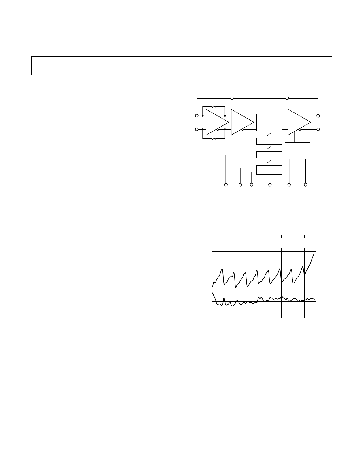
FUNCTIONAL BLOCK DIAGRAM
VCC (7 PINS)
R1
DIFF OR
SINGLE
INPUT
AMP
R2
BUFFER
DATA CLK GND (11 PINS)
DATEN
AD8323
ATTENUATION
CORE
8
DECODE
8
DATA LATCH
8
SHIFT
REGISTER
AD8323
BYP
POWER
AMP
Z
DIFF =
OUT
75⍀
POWER-DOWN
LOGIC
PD SLEEP
V
V
OUT+
OUT–
GENERAL DESCRIPTION
The AD8323 is a low-cost, digitally controlled, variable gain amplifier optimized for coaxial line driving applications such as cable
modems that are designed to the MCNS-DOCSIS upstream
standard. An 8-bit serial word determines the desired output gain
over a 53.5 dB range resulting in gain changes of 0.7526 dB/LSB.
The AD8323 comprises a digitally controlled variable attenuator
of 0 dB to –53.5 dB, which is preceded by a low noise, fixed
gain buffer and is followed by a low distortion high power amplifier. The AD8323 accepts a differential or single-ended input
signal. The output is specified for driving a 75 Ω load, such as
coaxial cable.
Distortion performance of –56 dBc is achieved with an output
level up to 60 dBmV at 21 MHz bandwidth. A key performance
and cost advantage of the AD8323 results from the ability to maintain a constant 75 Ω output impedance during power-up and
power-down conditions. This eliminates the need for external 75 Ω
termination, resulting in twice the effective output voltage when
compared to a standard operational amplifier. In addition, this
device has a sleep mode function that reduces the quiescent
current to 4 mA.
The AD8323 is packaged in a low-cost 28-lead TSSOP, operates
from a single 5 V supply, and has an operational temperature
range of –40°C to +85°C.
–50
–55
–60
–65
DISTORTION – dBc
–70
–75
8 162432404856
0
GAIN CONTROL – DEC Code
FO = 42MHz
= 60dBmV @ MAX GAIN
P
O
HD3
HD2
64 72
Figure 1. Harmonic Distortion vs. Gain Control
REV. 0
Information furnished by Analog Devices is believed to be accurate and
reliable. However, no responsibility is assumed by Analog Devices for its
use, nor for any infringements of patents or other rights of third parties
which may result from its use. No license is granted by implication or
otherwise under any patent or patent rights of Analog Devices.
One Technology Way, P.O. Box 9106, Norwood, MA 02062-9106, U.S.A.
Tel: 781/329-4700 World Wide Web Site: http://www.analog.com
Fax: 781/326-8703 © Analog Devices, Inc., 2000
Page 2

AD8323–SPECIFICATIONS
(TA = 25ⴗC, VS = 5 V, RL = RIN = 75 ⍀, VIN = 116 mV p-p, V
transformer1 with an insertion loss of 0.5 dB @ 10 MHz unless otherwise noted.)
measured through a 1:1
OUT
Parameter Conditions Min Typ Max Unit
INPUT CHARACTERISTICS
Specified AC Voltage Output = 60 dBmV, Max Gain 116 mV p-p
Noise Figure Max Gain, f = 10 MHz 13.8 dB
Input Resistance Single-Ended Input 800 Ω
Differential Input 1600 Ω
Input Capacitance 2pF
GAIN CONTROL INTERFACE
Gain Range 52.5 53.5 54.5 dB
Maximum Gain Gain Code = 71 Dec 26.5 27.5 28.5 dB
Minimum Gain Gain Code = 0 Dec –27 –26 –25 dB
Gain Scaling Factor 0.7526 dB/LSB
OUTPUT CHARACTERISTICS
Bandwidth (–3 dB) All Gain Codes 100 MHz
Bandwidth Roll-Off f = 65 MHz 1.3 dB
Bandwidth Peaking f = 65 MHz 0 dB
Output Noise Spectral Density Max Gain, f = 10 MHz –34 dBmV in
160 kHz
Min Gain, f = 10 MHz –48 dBmV in
160 kHz
Power-Down Mode, f = 10 MHz –68 dBmV in
160 kHz
1 dB Compression Point Max Gain, f = 10 MHz 18.5 dBm
Differential Output Impedance Power-Up and Power-Down 75 ± 20% Ω
OVERALL PERFORMANCE
Second Order Harmonic Distortion f = 21 MHz, P
f = 42 MHz, P
f = 65 MHz, P
Third Order Harmonic Distortion f = 21 MHz, P
f = 42 MHz, P
f = 65 MHz, P
= 60 dBmV @ Max Gain –77 dBc
OUT
= 60 dBmV @ Max Gain –71 dBc
OUT
= 60 dBmV @ Max Gain –64 dBc
OUT
= 60 dBmV @ Max Gain –56 dBc
OUT
= 60 dBmV @ Max Gain –55 dBc
OUT
= 60 dBmV @ Max Gain –53 dBc
OUT
Gain Linearity Error f = 10 MHz, Code to Code ±0.3 dB
Output Settling to 1 mV
Due to Gain Change Min to Max Gain 60 ns
Due to Input Step Change Max Gain, V
= 0 V to 116 mV p-p 30 ns
IN
Signal Feedthrough Max Gain, PD = 0, f = 42 MHz –30 dBc
POWER CONTROL
Power-Up Settling Time to 1 mV Max Gain, V
Power-Down Settling Time to 1 mV Max Gain, V
Between Burst Transients
2
Equivalent Output = 31 dBmV 3 mV p-p
= 0 300 ns
IN
= 0 40 ns
IN
Equivalent Output = 60 dBmV 30 mV p-p
POWER SUPPLY
Operating Range 4.75 5 5.25 V
Quiescent Current Power-Up Mode 123 133 140 mA
Power-Down Mode 30 35 40 mA
Sleep Mode 2 4 7 mA
OPERATING TEMPERATURE –40 +85 °C
RANGE
NOTES
1
TOKO 617DB-A0070 used for above specifications. MACOM ETC-1-IT-15 can be substituted.
2
Between Burst Transients measured at the output of a 42 MHz diplexer.
Specifications subject to change without notice.
–2–
REV. 0
Page 3
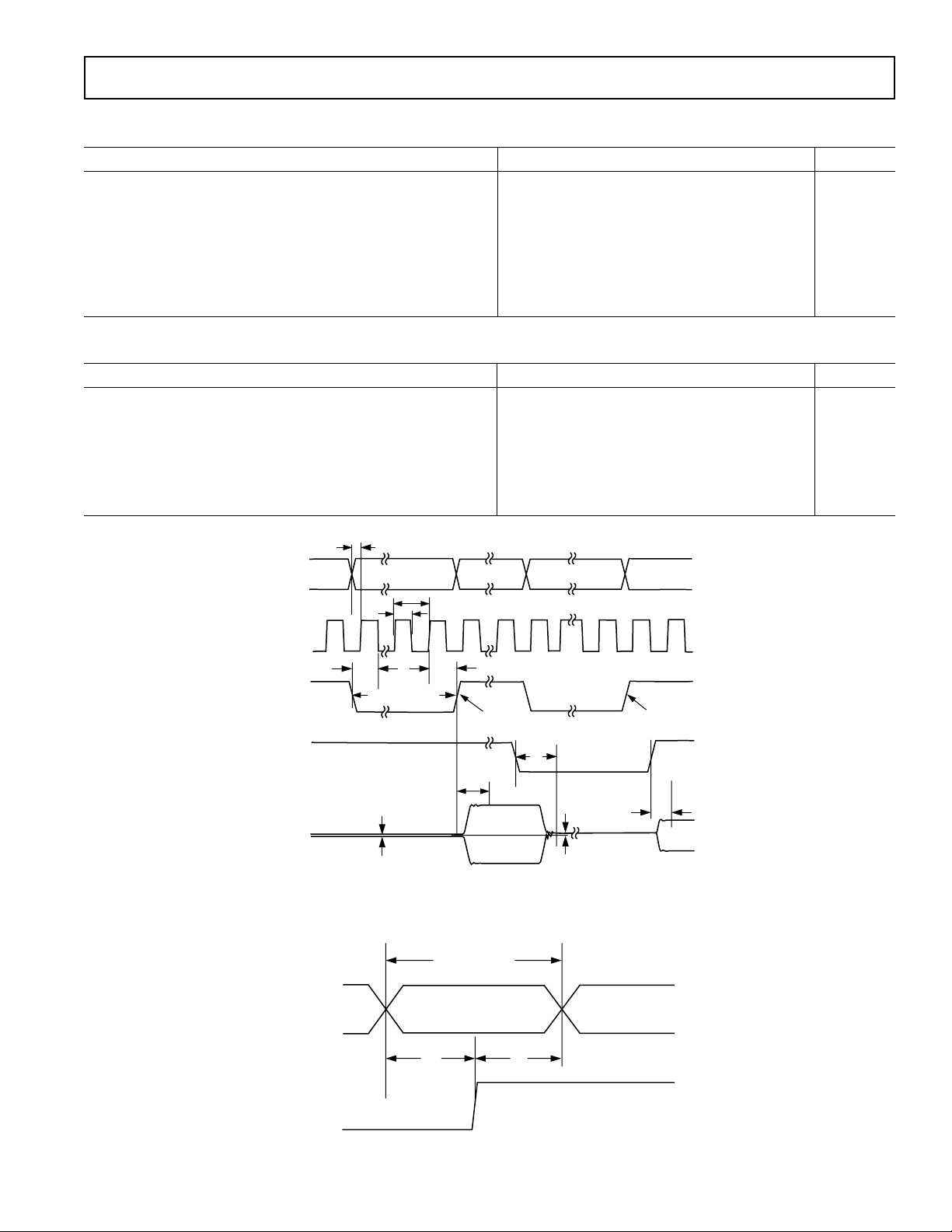
AD8323
VALID DATA BIT
MSB
MSB-1 MSB-2
T
DS
T
DH
SDATA
CLK
LOGIC INPUTS (TTL/CMOS Compatible Logic)
(DATEN, CLK, SDATA, PD, SLEEP, VCC = 5 V: Full Temperature Range)
Parameter Min Typ Max Unit
Logic “1” Voltage 2.1 5.0 V
Logic “0” Voltage 0 0.8 V
Logic “1” Current (V
Logic “0” Current (V
Logic “1” Current (V
Logic “0” Current (V
Logic “1” Current (V
Logic “0” Current (V
TIMING REQUIREMENTS
= 5 V) CLK, SDATA, DATEN 020nA
INH
= 0 V) CLK, SDATA, DATEN –600 –100 nA
INL
= 5 V) PD 50 190 µA
INH
= 0 V) PD –250 –30 µA
INL
= 5 V) SLEEP 50 190 µA
INH
= 0 V) SLEEP –250 –30 µA
INL
(Full Temperature Range, VCC = 5 V, TR = TF = 4 ns, f
= 8 MHz unless otherwise noted.)
CLK
Parameter Min Typ Max Unit
Clock Pulsewidth (T
Clock Period (T
Setup Time SDATA vs. Clock (T
Setup Time DATEN vs. Clock (T
Hold Time SDATA vs. Clock (T
Hold Time DATEN vs. Clock (T
) 16.0 ns
WH
) 32.0 ns
C
) 5.0 ns
DS
) 15.0 ns
ES
) 5.0 ns
DH
) 3.0 ns
EH
Input Rise and Fall Times, SDATA, DATEN, Clock (TR, TF)10ns
T
DS
SDATA
CLK
VALID DATA WORD G1
MSB. . . .LSB
T
C
T
WH
VALID DATA WORD G2
ANALOG
OUTPUT
DATEN
PD
SIGNAL AMPLITUDE (p-p)
T
ES
8 CLOCK CYCLES
T
EH
GAIN TRANSFER (G1)
T
GS
T
OFF
Figure 2. Serial Interface Timing
PEDESTAL
GAIN TRANSFER (G2)
T
ON
REV. 0
Figure 3. SDATA Timing
–3–
Page 4
AD8323
TOP VIEW
(Not to Scale)
28
27
26
25
24
23
22
21
20
19
18
17
16
15
1
2
3
4
5
6
7
8
9
10
11
12
13
14
AD8323
DATEN
GND
SDATA V
CC
CLK V
IN–
GND V
IN+
V
CC
GND
PD
V
CC
SLEEP
GND
GND BYP
V
CC
V
CC
V
CC
V
CC
GND GND
GND GND
GND GND
OUT– OUT+
WARNING!
ESD SENSITIVE DEVICE
ABSOLUTE MAXIMUM RATINGS*
Supply Voltage +V
S
PIN CONFIGURATION
Pins 5, 9, 10, 19, 20, 23, 27 . . . . . . . . . . . . . . . . . . . . . . 6 V
Input Voltages
Pins 25, 26 . . . . . . . . . . . . . . . . . . . . . . . . . . . . . . . . ±0.5 V
Pins 1, 2, 3, 6, 7 . . . . . . . . . . . . . . . . . . . . . –0.8 V to +5.5 V
Internal Power Dissipation
TSSOP . . . . . . . . . . . . . . . . . . . . . . . . . . . . . . . . . . . 0.9 W
Operating Temperature Range . . . . . . . . . . . –40° C to +85°C
Storage Temperature Range . . . . . . . . . . . . –65°C to +150°C
Lead Temperature, Soldering 60 seconds . . . . . . . . . . . 300°C
*Stresses above those listed under Absolute Maximum Ratings may cause perma-
nent damage to the device. This is a stress rating only; functional operation of the
device at these or any other conditions above those indicated in the operational
section of this specification is not implied. Exposure to absolute maximum rating
conditions for extended periods may affect device reliability.
ORDERING GUIDE
Model Temperature Range Package Description
JA
Package Option
AD8323ARU –40°C to +85°C 28-Lead TSSOP 67.7°C/W* RU-28
AD8323ARU-REEL –40°C to +85°C 28-Lead TSSOP 67.7°C/W* RU-28
AD8323-EVAL Evaluation Board
*Thermal Resistance measured on SEMI standard 4-layer board.
CAUTION
ESD (electrostatic discharge) sensitive device. Electrostatic charges as high as 4000 V readily
accumulate on the human body and test equipment and can discharge without detection. Although
the AD8323 features proprietary ESD protection circuitry, permanent damage may occur on
devices subjected to high-energy electrostatic discharges. Therefore, proper ESD precautions are
recommended to avoid performance degradation or loss of functionality.
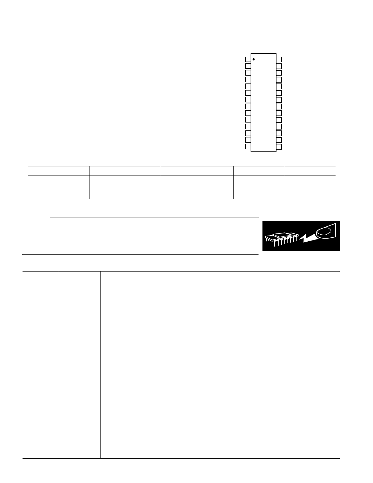
Pin No. Mnemonic Description
1 DATEN Data Enable Low Input. This port controls the 8-bit parallel data latch and shift register. A Logic
2 SDATA Serial Data Input. This digital input allows for an 8-bit serial (gain) word to be loaded into the
3 CLK Clock Input. The clock port controls the serial attenuator data transfer rate to the 8-bit master-
4, 8, 11,12, GND Common External Ground Reference.
13, 16, 17, 18,
22, 24, 28
5, 9, 10, 19, V
20, 23, 27
6 PD Logic “0” powers down the part. Logic “1” powers up the part.
7 SLEEP Low Power Sleep Mode. In the Sleep mode, the AD8323’s supply current is reduced to 4 mA. A
14 OUT– Negative Output Signal.
15 OUT+ Positive Output Signal.
21 BYP Internal Bypass. This pin must be externally ac-coupled (0.1 µF cap).
25 V
26 V
CC
IN+
IN–
PIN FUNCTION DESCRIPTIONS
0-to-1 transition transfers the latched data to the attenuator core (updates the gain) and simultaneously inhibits serial data transfer into the register. A 1-to-0 transition inhibits the data latch
(holds the previous gain state) and simultaneously enables the register for serial data load.
internal register with the MSB (Most Significant Bit) first.
slave register. A Logic 0-to-1 transition latches the data bit and a 1-to-0 transfers the data bit to
the slave. This requires the input serial data word to be valid at or before this clock transition.
Common Positive External Supply Voltage. A 0.1 µF capacitor must decouple each pin.
Logic “0” powers down the part (High Z
State) and a Logic “1” powers up the part.
OUT
Noninverting Input. DC-biased to approximately VCC/2. For single-ended inverting operation,
use a 0.1 µF decoupling capacitor and a 39.2 Ω resistor between V
and ground.
IN+
Inverting Input. DC-biased to approximately VCC/2. Should be ac-coupled with a 0.1 µF capacitor.
–4–
REV. 0
Page 5
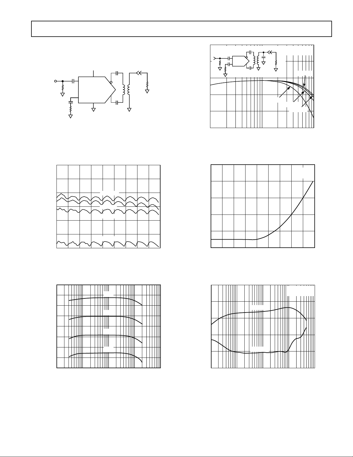
Typical Performance Characteristics–
GAIN CONTROL – Decimal
OUTPUT NOISE – dBmV in 160kHz
–30
0
–34
–38
–42
–46
–50
8 16 2432 4048 566472
f = 10MHz
PD = 1
FREQUENCY – MHz
FEEDTHROUGH – dB
0
0.1
–20
–40
–60
–80
–100
1 10 100
1k
MAX GAIN
MIN GAIN
PD = 0
V
IN
= 116mV p-p
AD8323
GAIN ERROR – dB
–0.5
1.5
1.0
0.5
0.0
V
IN
R
V
CC
0.1F
V
IN–
V
IN+
GND
TI
0.1F
39.2⍀
82.5⍀
TPC 1. Basic Test Circuit
TOKO 617DB–A0070
0.1F
OUT–
OUT+
0.1F
f = 10MHz
f = 5MHz
f = 42MHz
1:1
OUT
34
IN
31
28
R
75⍀
L
GAIN – dB
25
V
IN–
V
IN+
1:1
OUT
C
L
CL = 50pF
22
19
1 10 100
FREQUENCY – MHz
R
L
75⍀
CL = 20pF
P
= 60dBmV
OUT
@ MAX GAIN
CL = 0pF
CL = 10pF
TPC 4. AC Response for Various Cap Loads
–1.0
–1.5
0
8 16 24 32404856
TPC 2. Gain Error vs. Gain Control
40
30
20
10
0
GAIN – dB
–10
–20
–30
–40
0.1
1 10 100 1k
TPC 3. AC Response
f = 65MHz
GAIN CONTROL – Decimal
71D
46D
23D
00D
FREQUENCY – MHz
64 72
TPC 5. Output Referred Noise vs. Gain Control
TPC 6. Input Signal Feedthrough vs. Frequency
REV. 0
–5–
Page 6

AD8323
–60
–65
P
= 62dBmV
OUT
@ MAX GAIN
P
= 61dBmV
–70
–75
DISTORTION – dBc
–80
–85
5
OUT
@ MAX GAIN
P
= 60dBmV
OUT
@ MAX GAIN
P
= 58dBmV
OUT
@ MAX GAIN
15 25 35 45 55 65
FUNDAMENTAL FREQUENCY – MHz
TPC 7. Second Order Harmonic Distortion vs. Frequency
for Various Output Levels
–45
P
= 62dBmV
OUT
–50
–55
@ MAX GAIN
P
= 61dBmV
OUT
@ MAX GAIN
85
80
75
70
IMPEDANCE – ⍀
65
60
55
1
FREQUENCY – MHz
PD = 0
PD = 1
10 100
TPC 10. Input Impedance vs. Frequency
80
75
70
65
PD = 1
PD = 0
RTI = 82.5⍀
DISTORTION – dBc
–60
–65
5
15 25 35 45 55 65
P
= 60dBmV
OUT
@ MAX GAIN
P
= 58dBmV
OUT
@ MAX GAIN
FUNDAMENTAL FREQUENCY – MHz
TPC 8. Third Order Harmonic Distortion vs. Frequency for
Various Output Levels
60
50
40
30
20
10
– dBmV
OUT
P
–10
–20
–30
–40
0
41.4 41.8 42.2 42.6 43.0
41.2 41.6 42.0 42.4 42.8
41.0
FREQUENCY – MHz
P
= 60dBmV
OUT
@ MAX GAIN
TPC 9. Two-Tone Intermodulation Distortion
IMPEDANCE – ⍀
60
55
50
1
10 100
FREQUENCY – MHz
TPC 11. Output Impedance vs. Frequency
140
130
120
110
100
– mA
CC
+I
90
80
70
60
50
40
30
20
–50
–25 0 25 50 75 100
PD = 1
PD = 0
TEMPERATURE – ⴗC
TPC 12. Supply Current vs. Temperature
–6–
REV. 0
Page 7

AD8323
APPLICATIONS
General Application
The AD8323 is primarily intended for use as the upstream
power amplifier (PA) in DOCSIS (Data Over Cable Service
Interface Specifications) certified cable modems and CATV settop boxes. Upstream data is modulated in QPSK or QAM format, and done with DSP or a dedicated QPSK/QAM modulator.
The amplifier receives its input signal from the QPSK/QAM
modulator or from a DAC. In either case the signal must be
low-pass filtered before being applied to the amplifier. Because
the distance from the cable modem to the central office will vary
with each subscriber, the AD8323 must be capable of varying its
output power by applying gain or attenuation to ensure that all
signals arriving at the central office are of the same amplitude.
The upstream signal path contains components such as a transformer and diplexer that will result in some amount of power loss.
Therefore, the amplifier must be capable of providing enough
power into a 75 Ω load to overcome these losses without sacrificing the integrity of the output signal.
Operational Description
The AD8323 is composed of four analog functions in the
power-up or forward mode. The input amplifier (preamp) can
be used single-ended or differentially. If the input is used in
the differential configuration, it is imperative that the input
signals are 180 degrees out of phase and of equal amplitudes.
This will ensure the proper gain accuracy and harmonic
performance. The preamp stage drives a vernier stage that
provides the fine tune gain adjustment. The 0.7526 dB step
resolution is implemented in this stage and provides a total of
approximately 5.25 dB of attenuation. After the vernier stage,
a DAC provides the bulk of the AD8323’s attenuation (8 bits
or 48 dB). The signals in the preamp and vernier gain blocks
are differential to improve the PSRR and linearity. A differential current is fed from the DAC into the output stage, which
amplifies these currents to the appropriate levels necessary
to drive a 75 Ω load. The output stage utilizes negative feedback to implement a differential 75 Ω output impedance. This
eliminates the need for external matching resistors needed in
typical video (or video filter) termination requirements.
SPI Programming and Gain Adjustment
Gain programming of the AD8323 is accomplished using a
serial peripheral interface (SPI) and three digital control lines,
DATEN, SDATA, and CLK. To change the gain, eight bits of
data are streamed into the serial shift register through the
SDATA port. The SDATA load sequence begins with a falling
edge on the DATEN pin, thus activating the CLK line. Although
the CLK line is now activated, no change in gain is yet observed
at the output of the amplifier. With the CLK line activated, data
on the SDATA line is clocked into the serial shift register Most
Significant Bit (MSB) first, on the rising edge of each CLK
pulse. Because only a 7-bit shift register is used, the MSB of the
8-bit word is a “don’t care” bit and is shifted out of the register
on the eighth clock pulse. A rising edge on the DATEN line
latches the contents of the shift register into the attenuator core
resulting in a well controlled change in the output signal level.
The serial interface timing for the AD8323 is shown in Figures 2
and 3. The programmable gain range of the AD8323 is –26 dB
to +27.5 dB and scales 0.7526 dB per least significant bit (LSB).
Because the AD8323 was characterized with a TOKO transformer,
the stated gain values already take into account the losses associated with the transformer.
The gain transfer function is as follows:
= 27.5 dB – (0.7526 dB × (71 – CODE)) for 0 ≤ CODE ≤ 71
A
V
where A
is the gain in dB and CODE is the decimal equivalent
V
of the 8-bit word.
Valid gain codes are from 0 to 71. Figure 4 shows the gain
characteristics of the AD8323 for all possible values in an 8-bit
word. Note that maximum gain is achieved at Code 71. From
Code 72 through 127 the 5.25 dB of attenuation from the vernier stage is being applied over every eight codes, resulting in
the sawtooth characteristic at the top of the gain range. Because
the eighth bit is a “don’t care” bit, the characteristic for codes 0
through 127 repeats from Codes 128 through 255.
28
21
14
7
0
GAIN – dB
–7
–14
–21
–28
32 64 96 128 160 192 224
0
GAIN CODE – Decimal
256
Figure 4. Gain vs. Gain Code
Input Bias, Impedance, and Termination
The V
V
CC
IN+
and V
inputs have a dc bias level of approximately
IN–
/2, therefore the input signal should be ac-coupled. The
differential input impedance is approximately 1600 Ω while the
single-ended input impedance is 800 Ω. If the AD8323 is being
operated in a single-ended input configuration with a desired
input impedance of 75 Ω, the V
IN+
and V
inputs should be
IN–
terminated as shown in Figure 5. If an input impedance other
than 75 Ω is desired, the values of R1 and R2 in Figure 5 can be
calculated using the following equations:
ZR
= 1 800
IN
RZR
21=
IN
ZIN = 75⍀
–
R1 = 82.5⍀
AD8323
+
R2 = 39.2⍀
Figure 5. Single-Ended Input Termination
REV. 0
–7–
Page 8

AD8323
Output Bias, Impedance, and Termination
The differential output pins V
a dc level of approximately V
and V
OUT+
/2. Therefore, the outputs should
CC
are also biased to
OUT–
be ac-coupled before being applied to the load. This may be
accomplished by connecting 0.1 µF capacitors in series with the
outputs as shown in the typical applications circuit of Figure 6.
The differential output impedance of the AD8323 is internally
maintained at 75 Ω, regardless of whether the amplifier is in
forward transmit mode or reverse power-down mode, eliminating the need for external back termination resistors. A 1:1
transformer (TOKO #617DB-A0070) is used to couple
the amplifier’s differential output to the coaxial cable while
maintaining a proper impedance match. If the output signal
is being evaluated on standard 50 Ω test equipment, a 75 Ω to
50 Ω pad must be used to provide the test circuit with the
correct impedance match.
Power Supply Decoupling, Grounding, and Layout
Considerations
Careful attention to printed circuit board layout details will
prevent problems due to associated board parasitics. Proper RF
design technique is mandatory. The 5 V supply power should be
delivered to each of the V
pins via a low impedance power bus
CC
to ensure that each pin is at the same potential. The power bus
should be decoupled to ground with a 10 µF tantalum capacitor
located in close proximity to the AD8323. In addition to the
10 µF capacitor, each V
pin should be individually decoupled to
CC
ground with a 0.1 µF ceramic chip capacitor located as close to
the pin as possible. The pin labeled BYP (Pin 21) should also be
decoupled with a 0.1 µF capacitor. The PCB should have a low-
impedance ground plane covering all unused portions of the
component side of the board, except in the area of the input and
output traces (see Figure 11). It is important that all of the
AD8323’s ground pins are connected to the ground plane to
ensure proper grounding of all internal nodes. The differential
input and output traces should be kept as short and symmetrical
as possible. In addition, the input and output traces should be
kept far apart in order to minimize coupling (crosstalk) through
the board. Following these guidelines will improve the overall
performance of the AD8323 in all applications.
Initial Power-Up
When the 5 V supply is first applied to the VCC pins of the
AD8323, the gain setting of the amplifier is indeterminate.
Therefore, as power is first applied to the amplifier, the PD pin
should be held low (Logic 0) thus preventing forward signal
transmission. After power has been applied to the amplifier, the
gain can be set to the desired level by following the procedure in
the SPI Programming and Gain Adjustment section. The PD
pin can then be brought from Logic 0 to 1, enabling forward
signal transmission at the desired gain level.
Asynchronous Power-Down
The asynchronous PD pin is used to place the AD8323 into
“Between Burst” mode while maintaining a differential output
impedance of 75 Ω. Applying a Logic 0 to the PD pin activates
the on-chip reverse amplifier, providing a 74% reduction in
consumed power. The supply current is reduced from approximately 133 mA to approximately 35 mA. In this mode of
operation, between burst noise is minimized and the amplifier
can no longer transmit in the upstream direction. In addition to
the PD pin, the AD8323 also incorporates an asynchronous
SLEEP pin, which may be used to place the amplifier in a high
output impedance state and further reduce the supply current to
approximately 4 mA. Applying a Logic 0 to the SLEEP pin
places the amplifier into SLEEP mode. Transitioning into or
out of SLEEP mode will result in a transient voltage at the output
of the amplifier. Therefore, use only the PD pin for DOCSIS
compliant “Between Burst” operation.
PD
SLEEP
5V
DATEN
SDATA
CLK
10F
25V
0.1F
0.1F
0.1F
AD8323TSSOP
DATEN
SDATA
CLK
GND1
V
CC
PD
SLEEP
GND2
V
1
CC
V
CC2
GND3
GND4
GND5
OUT–
0.1F 0.1F
GND11
V
CC6
V
IN–
V
IN+
GND10
V
CC5
GND9
BYP
V
CC4
V
CC3
GND8
GND7
GND6
OUT+
TOKO 617DB-A0070
TO DIPLEXER Z
0.1F
0.1F
0.1F
0.1F
0.1F
= 75⍀
IN
Figure 6. Typical Applications Circuit
–8–
0.1F
0.1F
165⍀
V
IN–
ZIN = 150⍀
V
IN+
REV. 0
Page 9

AD8323
Distortion, Adjacent Channel Power, and DOCSIS
In order to deliver 58 dBmV of high fidelity output power
required by DOCSIS, the PA should be able to deliver about
60 dBmV to 61 dBmV in order to make up for losses associated
with the transformer and diplexer. It should be noted that the
AD8323 was characterized with the TOKO 617DB-A0070
transformer. TPC 7 and TPC 8 show the AD8323 second and
third harmonic distortion performance versus fundamental
frequency for various output power levels. These figures are
useful for determining the inband harmonic levels from 5 MHz to
65 MHz. Harmonics higher in frequency will be sharply attenuated by the low-pass filter function of the diplexer. Another
measure of signal integrity is adjacent channel power or ACP.
DOCSIS section 4.2.9.1.1 states, “Spurious emissions from a
transmitted carrier may occur in an adjacent channel that could
be occupied by a carrier of the same or different symbol rates.”
Figure 7 shows the measured ACP for a 16 QAM, 60 dBmV
signal, taken at the output of the AD8323 evaluation board (see
Figure 13 for evaluation board schematic). The transmit channel width and adjacent channel width in Figure 7 correspond to
symbol rates of 160 K
. Table I shows the ACP results for
SYM/SEC
the AD8323 for all conditions in DOCSIS Table 4-7 “Adjacent
Channel Spurious Emissions.”
RBW 500 Hz RF ATT 40dB
–10
VBW 5 kHz
SWT 12s UNIT dBm
–20
–30
–40
–50
–60
–70
CL1
–80
CENTER 10 MHz 60 kHz SPAN 600 kHz
C0 C0
CL1
CH PWR 5.44 dBm
ACP UP –52.99 dB
ACP LOW –54.36 dB
CU1
CU1
F1
Figure 7. Adjacent Channel Power
Table I. ACP Performance for All DOCSIS Conditions
(All Values in dBc)
TRANSMIT
CHANNEL
SYMBOL RATE
160 K
SYM/SEC
320 K
SYM/SEC
640 K
SYM/SEC
1280 K
SYM/SEC
2560 K
SYM/SEC
160 K
SYM/SEC
–53.0
–52.7 –53.4 –53.8 –54.8 –55.4
–53.8 –52.9 –53.3 –53.6 –54.2
–53.7 –53.4 –53.0 –53.3 –53.5
–55.4 –54.0 –53.6 –53.1 –53.3
ADJACENT CHANNEL SYMBOL RATE
320 K
640 K
SYM/SEC
–53.8 –55.0 –56.6 –56.3
SYM/SEC
1280 K
SYM/SEC
2560 K
SYM/SEC
Noise and DOCSIS
At minimum gain, the AD8323’s output noise spectral density is
10 nV/√Hz measured at 10 MHz. DOCSIS Table 4-8, “Spurious
Emissions in 5 MHz to 42 MHz,” specifies the output noise for
various symbol rates. The calculated noise power in dBmV for
160 K
SYM/SECOND
is:
Comparing the computed noise power of –48 dBmV to the
8 dBmV signal yields –56 dBc, which meets the required level of
–53 dBc set forth in DOCSIS Table 4-8. As the AD8323’s gain is
increased from this minimum value, the output signal increases at a
faster rate than the noise, resulting in a signal to noise ratio that
improves with gain. In transmit disable mode, the output noise
spectral density computed over 160 K
SYM/SECOND
is 1.0 nV/√Hz
or –68 dBmV.
Evaluation Board Features and Operation
The AD8323 evaluation board (Part # AD8323-EVAL) and
control software can be used to control the AD8323 upstream
cable driver via the parallel port of a PC. A standard printer
cable connected between the parallel port and the evaluation
board is used to feed all the necessary data to the AD8323 by
means of the Windows-based, Microsoft Visual Basic control
software. This package provides a means of evaluating the
amplifier by providing a convenient way to program the gain/
attenuation as well as offering easy control of the amplifiers’
asynchronous PD and SLEEP pins. With this evaluation kit the
AD8323 can be evaluated with either a single-ended or differential
input configuration. The amplifier can also be evaluated with or
without the PULSE diplexer in the output signal path. To remove
the diplexer from the signal path, move the 0 Ω chip resistor at
JP5 so the output signal is directed away from the diplexer
and toward the CABLE port of the evaluation board. Also,
remove the 0 Ω resistor at JP4. A schematic of the evaluation
board is provided in Figure 13.
Overshoot on PC Printer Ports
The data lines on some PC parallel printer ports have excessive
overshoot that may cause communications problems when presented to the CLK pin of the AD8323 (TP5 on the evaluation
board). The evaluation board was designed to accommodate a
series resistor and shunt capacitor (R1 and C15) to filter the
CLK signal if required.
Transformer and Diplexer
A 1:1 transformer is needed to couple the differential outputs of
the AD8323 to the cable while maintaining a proper impedance
match. The specified transformer is available from TOKO (Part
# 617DB-A0070); however, MA/COM part # ETC-1-1T-15
can also be used. The evaluation board is equipped with the
TOKO transformer, but is also designed to accept the MA/
COM transformer. The PULSE diplexer included on the
evaluation board provides a high-order low-pass filter function,
typically used in the upstream path. The ability of the PULSE
diplexer to achieve DOCSIS compliance is neither expressed
nor implied by Analog Devices Inc. Data on the diplexer should
be obtained from PULSE.
Differential Inputs
The AD8323-EVAL evaluation board is designed to accommodate
a Mini-Circuits T1-6T-KK81 1:1 transformer for the purpose of
converting a single-ended (ground-referenced) input signal to
differential inputs. Figure 8 and the following paragraphs identify
two options for providing differential input signals to the AD8323
evaluation board.
REV. 0
10
20
log –
nV
Hz
2
×
160 60 48
kHz dBmV
+=
–9–
Page 10

AD8323
Single-Ended-to-Differential Input (Figure 8, Option 1)
Install the Mini-Circuits T1-6T-KK81 1:1 transformer in the
T1 location of the evaluation board. Place 0 Ω chip resistors at
locations JP1, JP2, and JP3 such that the signal coming in V
IN+
is directed toward the transformer and the differential signal
coming out of the transformer is directed toward TP13 and
TP14. For 75 Ω input impedance, install 39.2 Ω resistors in R5
and R6 located on the back side of the evaluation board. In this
configuration the input signal must be applied to the V
IN+
port
of the evaluation board from a single-ended 75 Ω signal source.
For input impedances other than 75 Ω, the correct value for R5
and R6 can be computed using the following equation:
R R R Desired pedance R5 6 2 800==
()
Differential Input (Figure 8, Option 2)
, Im
=×
()
If a differential signal source is available, it may be applied
directly to both the V
IN+
and V
input ports of the evaluation
IN–
board. In this case, 0 Ω chip resistors should be placed at locations R8, JP1, JP2, and JP3 such that the V
IN+
and V
signals
IN–
are directed toward TP13 and TP14. Referring to Figure 8,
Option 2, a differential input impedance of 150 Ω can be
achieved by using a 165 Ω resistor for R7. For input impedances other than 150 Ω, the correct value for R7 can be computed
using the following equation:
Desired pedance RIm =
DIFF IN
OPTION 1 DIFFERENTIAL INPUT TERMINATION
VIN+
VIN–
7 1600
()
R6
T1
R5
R7
AD8323
AD8323
Installing the Visual Basic Control Software
To install the “CABDRIVE_23” evaluation board control software, close all Windows applications and then run “SETUP.EXE”
located on Disk 1 of the AD8323 Evaluation Software. Follow
the on-screen instructions and insert Disk 2 when prompted to
do so. Enter the path of the directory into which the software
will be installed and select the button in the upper left corner to
complete the installation.
Running the Software
To invoke the control software, go to START -> PROGRAMS
-> CABDRIVE_23, or select the AD8323.EXE icon from the
directory containing the software.
Controlling the Gain/Attenuation of the AD8323
The slide bar controls the AD8323’s gain/attenuation, which is
displayed in dB and in V/V. The gain scales at 0.7526 dB per
LSB with the valid codes being from decimal 0 to 71. The gain
code (i.e., position of the slide bar) is displayed in decimal, binary,
and hexadecimal (see Figure 9).
POWER-UP, POWER-DOWN AND SLEEP
The “Power-Up” and “Power-Down” buttons select the mode
of operation of the AD8323 by controlling the logic level on the
asynchronous PD pin. The “Power-Up” button applies a
Logic 1 to the PD pin putting the AD8323 in forward transmit
mode. The “Power-Down” button applies a Logic 0 to the PD
pin selecting reverse mode, where the forward signal transmission
is disabled while a back termination of 75 Ω is maintained.
Checking the “Enable SLEEP Mode” box applies a Logic 0 to
the asynchronous SLEEP pin, putting the AD8323 into SLEEP
mode.
Memory Section
The “MEMORY” section of the software provides a convenient
way to alternate between two gain settings. The “X->M1” button stores the current value of the gain slide bar into memory
while the “RM1” button recalls the stored value, returning the
gain slide bar to that level. The “X->M2” and “RM2” buttons
work in the same manner.
OPTION 2 DIFFERENTIAL INPUT TERMINATION
Figure 8. Differential Input Termination Options
–10–
REV. 0
Page 11

EVALUATION BOARD FEATURES AND OPERATION
AD8323
REV. 0
Figure 9. Screen Display of Windows-Based Control Software
–11–
Page 12

AD8323
Figure 10. Evaluation Board—Assembly (Component Side)
Figure 11. Evaluation Board Layout (Component Side)
–12–
REV. 0
Page 13

AD8323
Figure 12. Evaluation Board—Solder Side
REV. 0
–13–
Page 14

AD8323
S2
IN–
V
AGND;3,4,5
R9
R8
0⍀
4
NC = 5
312
3
JP1
A
2
B
1
YEL
TP14
R5
C13
0.1F
0.1F
0.1F
C8
C7
28272625242322212019181716
IN–
IN+
CC6
V
V
V
GND11
DATEN
123456789
DATEN
RED
C18
TP15
10F
+
1
CC
V
J1
SDATA
SDATA
25V
TP20
CLK
CLK
BLK
GND1
C1
GND10
VCCPD
0.1F
1
J2
DNI
82.5⍀
V
C6
CC5
U1
PD
1:1
R7
0.1F
BYP
GND9
SLEEP
GND2
SLEEP
AGND
1
6
T1 DNI
1
DNI
C12
0.1F
C5
CC4
CC3
V
V
GND8
CC1VCC2
V
GND3
1011121314
C4
C3
0.1F
S3
IN+
V
G9
10
G8
11
G7
AGND;3,4,5
12
G6
13
G5
14
G4
B
3
JP3 JP2
B
0.1F
C2
GND7
GND4
0.1F
15
2
16
17
3
18
AA
2
YEL
TP13
R6
39.2⍀
0.1F
15
OUT+
GND6
AD8323TSSOP
GND5
OUT–
G3
G2
G1
TP3
U2
DNI
TP9
DNI
TP11
C11
DNI
TP12
PD
WHT
TP6
DNI
C14
R2
0⍀
WHT
TP4
DATEN
WHT
TP1
P1P1P1P1P1P1P1P1P1P1P1P1P1P1P1P1P1
123456789
1920212223242526272829303132333435
AMP-552742
P1P1P1P1P1P1P1P1P1P1P1P1P1P1P1P1P1
S4
HPP
TP21
DNI
OUT = 2,4,6,7,8
PULSEB5008
9
TP22
DNI
B
5
A–B
3
A
1
4
NC = 2
TOKO-B4FETCC1-1T
5
4
312
0.1F
CLK
WHT
TP5
C15
R1
0⍀
WHT
TP2
SDATA
WHT
S1
CABLE
AGND;3,4,5
TP10
DNI
JP4
1
JP5
B
2
3
A
3
1:1
T2B
1
5
1:1
T2A DNI
C10
0.1F
SLEEP
WHT
TP16
DNI
C16
0⍀
R11
WHT
TP17
101112131415161718
AGND;3,4,5
R3
0⍀
TP8
TP7
WHT
TP18
DNI
R12
TP19
R4
DNI
DNI
SPARE
0⍀
WHT
DNI
C17
DNI
P1
36
P1
Figure 13. Evaluation Board Schematic
–14–
REV. 0
Page 15

AD8323
EVALUATION BOARD BILL OF MATERIALS
AD8323 Evaluation Board Rev. C SINGLE-ENDED INVERTING INPUT – Revised – June 22, 2000
Qty. Description Vendor Ref Desc.
1 10 µF 16 V. ‘C’ size tantalum chip capacitor ADS# 4-7-6 C18
12 0.1 µF 50 V. 1206 size ceramic chip capacitor ADS# 4-5-18 C1–8, 10–13
60 Ω 1/8 W. 1206 size chip resistor ADS# 3-18- 88 R1–3, 8, 11, 12
1 39.2 Ω 1% 1/8 W. 1206 size chip resistor ADS# 3-18-113 R6
1 82.5 Ω 1% 1/8 W. 1206 size chip resistor ADS# 3-18-189 R5
2 Yellow Test Point [INPUTS] (Bisco TP104-01-04) ADS# 12-18-32 TP13, 14
10 White Test Point [DATA] (Bisco TP104-01-09) ADS# 12-18-42 TP1–6, 16–19
1 Red Test Point [V
1 Black Test Point [A.GND] (Bisco TP104-01-00) ADS# 12-18-44 TP20
30Ω 0805 size chip resistors ADS# 3-27-22 JP1–3
475Ω right-angle BNC Telegartner # J01003A1949 ADS# 12-6-28 VIN+, VIN–, HPP, CABLE
1 Centronics type 36 pin Right-Angle Connector ADS# 12-3-50 P1
2 5-way Metal Binding Post (E F Johnson # 111-2223-001) ADS# 12-7-7 VCC, GND
1 1:1 Transformer TOKO # 617DB - A0070 TOKO T2 B
1 Diplexer PULSE* PULSE U2
1 AD8323 (TSSOP) UPSTREAM Cable Driver ADI# AD8323XRU U1
1 AD8323 REV. C Evaluation PC board D C S Evaluation PC Board
4 #4 - 40 × 1/4 inch STAINLESS panhead machine screw ADS# 30-1-1
4 #4 - 40 × 3/4 inch long aluminum round stand-off ADS# 30-16-3
2 # 2 - 56 × 3/8 inch STAINLESS panhead machine screw ADS# 30-1-17 (p1 hardware)
2 # 2 steel flat washer ADS# 30-6-6 (p1 hardware)
2 # 2 steel internal tooth lockwasher ADS# 30-5-2 (p1 hardware)
3 # 2 STAINLESS STEEL hex. machine nut ADS# 30-7-6 (p1 hardware)
DO NOT INSTALL C14–C17, R4, R7, R9, T1, T2A, TP7–TP12, TP21, TP22.
*PULSE Diplexer part #’s B5008 (42 MHz), CX6002 (42 MHz), B5009 (65 MHz).
] (Bisco TP104-01-02) ADS# 12-18-43 TP15
CC
REV. 0
–15–
Page 16

AD8323
OUTLINE DIMENSIONS
Dimensions shown in inches and (mm).
28-Lead TSSOP
(RU-28)
0.386 (9.80)
0.378 (9.60)
PIN 1
0.006 (0.15)
0.002 (0.05)
SEATING
PLANE
28
0.0256 (0.65)
BSC
0.0118 (0.30)
0.0075 (0.19)
15
0.177 (4.50)
0.169 (4.30)
141
0.0433 (1.10)
MAX
0.0079 (0.20)
0.0035 (0.090)
0.256 (6.50)
0.246 (6.25)
8ⴗ
0ⴗ
C02045–2.5–7/00 (Rev. 0)
0.028 (0.70)
0.020 (0.50)
–16–
PRINTED IN U.S.A.
REV. 0
 Loading...