

Page 1
Gain Programmable
GAIN CONTROL – Decimal
DISTORTION – dBc
–90
0 8 16 24 32 40 48 56 64 72
–80
–70
–60
–50
–40
fO = 42MHz
V
IN
= 137mV p-p
(P
IN
= –15dBm)
(P
OUT
= 11dBm @
MAX GAIN)
HD3
HD2
a
FEATURES
Linear in dB Gain Response Over >53 dB Range
Drives Low Distortion >11 dBm Signal into 75 ⍀ Load:
–53 dBc SFDR at 42 MHz
Very Low Output Noise Level
Maintains Constant 75 ⍀ Output Impedance
Power-Up and Power-Down Condition
No Line Transformer Required
Upper Bandwidth: 235 MHz (Min Gain)
9 V Single Supply Operation
Power-Down Functionality
Supports SPI Interface
Low Cost
APPLICATIONS
Gain Programmable Line Driver
HFC High Speed Data Modems
Interactive CATV Set-Top Boxes
CATV Plant Test Equipment
General Purpose IF Variable Gain Block
VIN+
VIN–
CATV Line Driver
FUNCTIONAL BLOCK DIAGRAM
AD8321
INV
DATEN CLK
ATTENUATOR CORE
DATA LATCH
DATA SHIFT REGISTER
DATA SHIFT REGISTER
SDATA
AD8321
GNDVCC
PWR
AMP
REVERSE
AMP
POWER-
DOWN/
SWITCH
INTER
VOUT
PD
DESCRIPTION
The AD8321 is a low cost digitally controlled variable gain
amplifier optimized for coaxial line driving applications such as
cable modems that are designed to the DOCSIS* (upstream)
standard. An 8-bit serial word determines the desired output
gain over a 53.4 dB range, resulting in gain changes of 0.75 dB/
LSB.
The AD8321 comprises a digitally controlled variable attenuator
of 0 dB to –53.4 dB, which is preceded by a low noise, fixed
gain buffer and followed by a low distortion high power amplifier. The AD8321 accepts a differential or single-ended input
signal. The output is specified for driving a 75 Ω load, such as
coaxial cable, although the AD8321 is capable of driving other
loads. Performance of –53 dBc is achieved with an output level
up to 11 dBm at 42 MHz bandwidth using a 9 V supply.
A key performance and cost advantage of the AD8321 results
from the ability to maintain a constant 75 Ω output impedance
during power-up and power-down conditions. This eliminates
the need for external 75 Ω termination, resulting in twice the
effective output voltage when compared to a standard operational amplifier, thus eliminating the need for a transformer.
*Data-Over-Cable Service Interface Specifications
The AD8321 is packaged in a low cost 20-lead SOIC, operates
from a single +9 V supply, and has an operational temperature
range of –40°C to +85°C.
Figure 1. Harmonic Distortion vs. Gain Control
REV. 0
Information furnished by Analog Devices is believed to be accurate and
reliable. However, no responsibility is assumed by Analog Devices for its
use, nor for any infringements of patents or other rights of third parties
which may result from its use. No license is granted by implication or
otherwise under any patent or patent rights of Analog Devices.
One Technology Way, P.O. Box 9106, Norwood, MA 02062-9106, U.S.A.
Tel: 781/329-4700 World Wide Web Site: http://www.analog.com
Fax: 781/326-8703 © Analog Devices, Inc., 1999
Page 2

(@ VCC = +9 V, TA = +25ⴗC, VIN = 0.137 V p-p, single-ended input, RL = 75 ⍀, RIN =
AD8321–SPECIFICATIONS
75 ⍀ unless otherwise noted)
Parameter Conditions Min Typ Max Units
INPUT CHARACTERISTICS
Specified AC Voltage Output = 11 dBm, Max Gain 0.137 V p-p
Noise Figure Max Gain, f = 10 MHz 15 dB
Input Resistance Single-Ended Input 820 Ω
Differential Input 900 Ω
Input Capacitance 2.0 pF
GAIN CONTROL INTERFACE
Gain Range 52.4 53.4 54.4 dB
Maximum Gain 25.25 26 26.75 dB
Minimum Gain –28.15 –27.4 –26.4 dB
Gain Scaling Factor 0.7526 dB/LSB
OUTPUT CHARACTERISTICS
Bandwidth (–3 dB) All Gain Codes 120 MHz
Bandwidth Roll-Off f = 65 MHz 0.8 dB
Bandwidth Peaking f = 65 MHz 0 dB
Output Offset Voltage All Gain Codes, Full Temperature Range ±30 mV
Output Noise Spectral Density Max Gain, f = 10 MHz 60 nV/√Hz
Min Gain, f = 10 MHz 20 nV/√Hz
Output Noise Temperature Sensitivity 0 ≤ T
≤ +70°C, Min Gain 0.02 nV/√Hz/°C
A
Power-Down Spectral Density 1 nV/√Hz
1 dB Compression Point Max Gain, f = 10 MHz +19.5 dBm
Output Impedance Power-Up and Power-Down 60 75 90 Ω
OVERALL PERFORMANCE
Worst Harmonic Distortion f = 42 MHz, P
f = 65 MHz, P
Distortion Temperature Sensitivity –40°C ≤ T
A
= 11 dBm, VCC = +9 V –53 dBc
OUT
= 11 dBm, VCC = +9 V –51 dBc
OUT
≤ +85°C 0.03 dBc/°C
Gain Accuracy f = 10 MHz, All Gain Codes ±0.2 dB
Gain Temperature Sensitivity 0 ≤ T
≤ +70°C 0.004 dB/°C
A
Output Settling to 1 mV
Gain Change @ T
Input Change Max Gain, V
= 1 Min to Max Gain, VIN = 0 V 60 ns
DATEN
= 0.15 V Step 30 ns
IN
Signal Feedthrough Power Down, 65 MHz, Min Gain –80 dBc
VIN = 0.137 V p-p
POWER CONTROL
Power-Down Settling Time to 1 mV Max Gain, V
Power-Up Settling Time to 1 mV Max Gain, V
Power-Up/Down Pedestal Offset Max Gain, V
= 0 40 ns
IN
= 0 300 ns
IN
= 0 ±30 mV
IN
Power-Up/Down Glitch Max Gain, VIN = 0 40 mV p-p
POWER SUPPLY
Quiescent Current Power-Up, V
= +9 V 82 90 97 mA
CC
Power-Down, VCC = +9 V 45 52 60 mA
Specifications subject to change without notice.
–2–
REV. 0
Page 3
AD8321
LOGIC INPUTS (TTL/CMOS Logic)
(DATEN, CLK, SDATA, VCC = +9 V; Full Temperature Range)
Parameter Min Typ Max Units
Logic “1” Voltage 2.1 5.0 V
Logic “0” Voltage 0 0.8 V
Logic “1” Current (V
Logic “0” Current (V
Logic “1” Current (V
Logic “0” Current (V
TIMING REQUIREMENTS
= 5 V) CLK, SDATA, DATEN 020nA
INH
= 0 V) CLK, SDATA, DATEN –600 –100 nA
INL
= 5 V) PD 50 190 µA
INH
= 0 V) PD –250 –30 µA
INL
(Full Temperature Range, VCC = +9 V, TR = TF = 4 ns, f
= 8 MHz unless otherwise noted.)
CLK
Parameter Min Typ Max Units
Clock Pulsewidth (T
Clock Period (T
Setup Time SDATA vs. Clock (T
Setup Time DATEN vs. Clock (T
Hold Time SDATA vs. Clock (T
Hold Time DATEN vs. Clock (T
) 16.0 ns
WH
) 32.0 ns
C
) 5.0 ns
DS
) 15.0 ns
ES
) 5.0 ns
DH
) 3.0 ns
EH
Input Rise and Fall Times, SDATA, DATEN, Clock (TR, TF)10ns
T
DS
SDATA
CLK
VALID DATA WORD G1
MSB. . . .LSB
T
C
T
WH
VALID DATA WORD G2
DATEN
PD
ANALOG
OUTPUT
T
ES
8 CLOCK CYCLES
SIGNAL AMPLITUDE (p-p)
Figure 2. Serial Interface Timing
SDATA
MSB
CLK
T
EH
GAIN TRANSFER (G1)
T
GS
VALID DATA BIT
MSB-1 MSB-2
T
DS
T
T
DH
OFF
PEDESTAL
GAIN TRANSFER (G2)
T
ON
Figure 3. SDATA Timing
–3–REV. 0
Page 4
AD8321
ABSOLUTE MAXIMUM RATINGS*
Supply Voltage +V
S
Pins 7, 8, 9, 17, 20 . . . . . . . . . . . . . . . . . . . . . . . . . . . +11 V
Input Voltages
Pins 18, 19 . . . . . . . . . . . . . . . . . . . . . . . . . . . . . . . . ±0.5 V
Pins 1, 2, 3, 6 . . . . . . . . . . . . . . . . . . . . . . –0.8 V to +5.5 V
Internal Power Dissipation
Small Outline (R) . . . . . . . . . . . . . . . . . . . . . . . . . . . 0.90 W
Operating Temperature Range . . . . . . . . . . . –40°C to +85°C
Storage Temperature Range . . . . . . . . . . . . –65°C to +150°C
Lead Temperature, Soldering 60 seconds . . . . . . . . . . +300°C
*Stresses above those listed under Absolute Maximum Ratings may cause perma-
nent damage to the device. This is a stress rating only; functional operation of the
device at these or any other conditions above those indicated in the operational
section of this specification is not implied. Exposure to absolute maximum rating
conditions for extended periods may affect device reliability.
PIN CONFIGURATION
SDATA
CLK
DATEN
GND
BYP1
PD
VCC
VCC
VCC
VOUT
1
2
3
4
5
AD8321
TOP VIEW
6
(Not to Scale)
7
8
9
10
20
VCC
19
VIN–
18
VIN+
17
VCC
16
GND
15
GND
14
BYP2
13
GND
12
GND
11
GND
ORDERING GUIDE
Model Temperature Range Package Description
JA
Package Option
AD8321AR –40°C to +85°C 20-Lead SOIC 58°C/W* R-20
AD8321AR-REEL –40°C to +85°C 20-Lead SOIC 58°C/W* R-20
AD8321-EVAL Evaluation Board
*Thermal Resistance measured on SEMI standard 4-layer board.
CAUTION
ESD (electrostatic discharge) sensitive device. Electrostatic charges as high as 4000 V readily
accumulate on the human body and test equipment and can discharge without detection.
WARNING!
Although the AD8321 features proprietary ESD protection circuitry, permanent damage may
occur on devices subjected to high energy electrostatic discharges. Therefore, proper ESD
precautions are recommended to avoid performance degradation or loss of functionality.
ESD SENSITIVE DEVICE
PIN FUNCTION DESCRIPTIONS
Pin Function Description
1 SDATA Serial Data Input. This digital input allows for an 8-bit serial (gain) word to be loaded into the internal
register with the MSB (most significant bit) first.
2 CLK Clock Input. The clock port controls the serial attenuator data transfer rate to the 8-bit master-slave
register. A Logic 0-to-1 transition latches the data bit and a 1-to-0 transfers the data bit to the slave.
This requires the input serial data word to be valid at or before this clock transition.
3 DATEN Data Enable Low Input. This port controls the 8-bit parallel data latch and shift register. A Logic 0-to-
1 transition transfers the latched data to the attenuator core (updates the gain) and simultaneously
inhibits serial data transfer into the register. A 1-to-0 transition inhibits the data latch (holds the previous gain state) and simultaneously enables the register for serial data load.
4, 11, 12,
13, 15, 16 GND Common External Ground Reference.
5 BYP1 V
/2 Reference Pin. A dc output reference level that is equal to 1/2 of the supply voltage (VCC). This
CC
port should be externally ac-decoupled (0.1 µF capacitor). For external use of this reference voltage,
buffering is required.
6 PD Power-Down Low Logic Input. A Logic 0 powers down (shuts off) the power amplifier disabling the
output signal and enabling the reverse amplifier. A Logic 1 enables the output power amplifier and
disables the reverse amplifier.
7, 8, 9, 17, 20 VCC Common Positive External Supply Voltage.
10 VOUT Output Signal Port. DC-biased to approximately V
CC
/2.
14 BYP2 Internal Bypass. This pin must be externally ac-decoupled (0.1 µF cap).
18 VIN+ Noninverting Input. DC-biased to approximately V
/2. For single-ended inverting operation, use
CC
0.1 µF decoupling capacitor between VIN+ and ground.
19 VIN– Inverting Input. DC-biased to approximately V
/2. Should be ac-coupled with a 0.1 µF capacitor.
CC
–4–
REV. 0
Page 5
Typical Performance Characteristics–AD8321
FREQUENCY – MHz
3RD ORDER INTERCEPT – dBm
5
22
23
24
25
27
PO = 11dBm
MAX GAIN
26
15 25
35 45
55
28
29
30
65
0.6
0.3
0
–0.3
–0.6
GAIN ERROR – dB
–0.9
–1.2
08
f = 10MHz
f = 42MHz
f = 65MHz
16 24 32 40 48 56 64 72
GAIN CONTROL – Decimal
Figure 4. Gain Error vs. Gain Control
70
PD = 1
60
50
40
30
OUTPUT NOISE – nV/ Hz
20
10
MAX GAIN
(71D)
MIN GAIN
(00D)
1 10 100
FREQUENCY – MHz
Figure 7. Output Referred Noise vs.
Frequency
30
–10
GAIN – dB
–20
–30
–40
20
10
0
0.1
1 10 100
FREQUENCY – MHz
71D
46D
23D
00D
Figure 5. AC Response
–30
–40
–50
–60
DISTORTION – dBc
–70
–80
0816
GAIN CONTROL – Decimal
fO = 65MHz
= 0.137V p-p
V
IN
(P
= –15dBm)
IN
(P
= 11dBm @
OUT
MAX GAIN)
HD2
24 40 48 56 64 72
32
Figure 8. Harmonic Distortion vs.
Gain Control
HD3
1000
70
60
50
40
30
OUTPUT NOISE – nV/ Hz
20
10
08
16 24 32 40 48 56 64 72
GAIN CONTROL – Decimal
f = 10MHz
PD =1
Figure 6. Output Referred Noise vs.
Gain Control
–47
PIN = –14dBm
= 12dBm @
(P
OUT
MAX GAIN)
–50
PIN = –13dBm
= 13dBm @
(P
OUT
MAX GAIN)
–53
DISTORTION – dBc
–56
–59
5 15 25 45 55 65
FUNDAMENTAL FREQUENCY – MHz
PIN = –15dBm
(P
OUT
MAX GAIN)
PIN = –17dBm
(P
OUT
MAX GAIN)
35
= 11dBm @
= 9dBm @
Figure 9. Second Order Harmonic
Distortion vs. Frequency for Various
Input Levels
–47
PIN = –13dBm
(P
MAX GAIN)
–50
–53
DISTORTION – dBc
–56
–59
5 15 25 45 55 65
Figure 10. Third Order Harmonic
Distortion vs. Frequency for Various
Input Levels
REV. 0
= 13dBm @
OUT
FUNDAMENTAL FREQUENCY – MHz
PIN = –14dBm
= 12dBm @
(P
OUT
MAX GAIN)
PIN = –15dBm
= 11dBm @
(P
OUT
MAX GAIN)
PIN = –17dBm
= 9dBm @
(P
OUT
MAX GAIN)
35
20
0
–20
– dBm
OUT
–40
P
–60
–80
41.0
41.4 41.8 42.2 42.6 43.0
FREQUENCY – MHz
PO = 11dBm
MAX GAIN
Figure 11. Two-Tone Intermodulation Distortion
–5–
Figure 12. Third Order Intercept vs.
Frequency
Page 6
AD8321
34
30
26
GAIN – dB
22
18
14
1 10 100
FREQUENCY – MHz
MAX GAIN
= 11dBm
P
O
CL = 10pF
CL = 0pF
CL = 20pF
CL = 50pF
Figure 13. AC Response for Various
Capacitor Loads
7.5mV
V
OUT
VIN = 0V p-p
MAX GAIN
tr(CLK) = 3ns
CLK
DATEN
5V
150ns
Figure 16. Clock Feedthrough
5mV
5V
V
OUT
MIN GAIN
V
= 0V p-p
IN
PD
75ns
Figure 14. Power Up/Power Down
Glitch
0
–20
–40
–60
FEEDTHROUGH – dB
–80
–100
0.1
1 10 100
FREQUENCY – MHz
PD = 0
MAX GAIN
MIN GAIN
1000
Figure 17. Input Signal Feedthrough
vs. Frequency
15mV
5V
V
OUT
MAX GAIN
= 0V p-p
V
IN
PD
75ns
Figure 15. Power Up/Power Down
Glitch
0.75V
V
OUT
V
IN
200mV
MAX GAIN
V
= 0V p-p – 0.137V p-p
IN
30ns
Figure 18. Output Settling Time Due
to Input Change
1.5V
V
V
OUT
IN
0.5V
MAX GAIN
30ns
Figure 19. Overload Recovery
90
85
80
75
70
IMPEDANCE – V
65
60
1 10 100
PD = 0
PD = 1
FREQUENCY – MHz
Figure 20. Output Impedance vs.
Frequency
100
90
80
– mA
70
CC
+I
60
50
40
–50
–25 0 25
PD =1
PD = 0
50 75 100
TEMPERATURE – 8C
Figure 21. Supply Current vs.
Temperature
–6–
REV. 0
Page 7

AD8321
OPERATIONAL DESCRIPTION
The AD8321 is a digitally controlled variable gain power ampli-
fier that is optimized for driving a 75 Ω cable. As a multifunc-
tional bipolar device on a single silicon die, it incorporates all
the analog features necessary to accommodate reverse path
(upstream) high speed (5 MHz to 65 MHz) cable data modem
requirements. The AD8321 has an overall gain range of approximately 53 dB and is capable of greater than 100 MHz
operation at output signal levels exceeding 12 dBm. Overall,
when considering the device’s wide gain range, low distortion,
wide bandwidth and variable load drive, the device can be used
in many variable gain block applications.
GNDVCC
PWR
AMP
REVERSE
AMP
POWER-
DOWN/
SWITCH
INTER
VOUT
PD
VIN+
VIN–
INV
DATEN CLK
AD8321
ATTENUATOR CORE
DATA SHIFT REGISTER
DATA SHIFT REGISTER
DATA LATCH
SDATA
Figure 22. Functional Block Diagram
The digitally programmable gain is controlled by the three-wire
“SPI” compatible inputs. These inputs are called SDATA
(serial data input port), DATEN (data enable low input port)
and CLK (clock input port). See Pin Function Descriptions
and Functional Block diagram. The AD8321 is programmed by
an 8-bit “attenuator” word. When a standard 8-bit word is
used, the first data bit MSB will be shifted out of the 7-bit shift
register during the eighth rising CLK edge. The lower seven
bits will then be loaded into the AD8321’s digital decode section when the DATEN input is taken high.
The gain of the AD8321 is linear in steps of 0.7526 dB. The
gain transfer function starts at –27.43 dB (at decimal code 0)
and increases 0.7526 dB/LSB. The gain increases up to decimal
code 71. At this point the gain is at its maximum level of 26 dB.
If a decimal word between 71 and 127 is entered, the gain is no
longer incremented and stays at 26 dB. Since the MSB of an 8-bit
word is a “don’t care” bit, at decimal code 128, the AD8321’s
gain returns to its minimum value. The gain vs. gain control
relationship repeats itself as shown in Figure 23 for the upper
127 codes.
The gain transfer function is as follows:
= 26 dB – ((71 – CODE) × 0.7526 dB) for CODE ≤ 71
A
V
A
= 26 dB for 71 ≤ CODE ≤ 127
V
= 26 dB + ((199 – CODE) × 0.7526 dB) for 128 ≤
A
V
CODE ≤ 199
A
= 26 dB for 199 ≤ CODE ≤ 255
V
where CODE is the decimal equivalent of the 8-bit word loaded in
the AD8321’s data latch (see Figure 23).
30
20
10
0
GAIN – dB
–10
–20
–30
32 22419216012864 96
0 256
GAIN CODE – Decimal
Figure 23. Linear-In dB Gain vs. Gain Control
The AD8321 is composed of four analog functions in the
power-up or forward mode. The input amplifier (preamp) which
can be used single-endedly or differentially and provides a maximum of 12 dB of attenuation. If the input is used in the differential configuration, it is imperative that the input signals are
180 degrees out of phase and of equal amplitudes. This will
ensure the proper gain accuracy and harmonic performance.
The preamp stage drives a vernier stage that provides the fine
tune gain adjustment. The 0.7526 dB step resolution is implemented in this stage. After the vernier stage, a DAC provides the
bulk of the AD8321’s attenuation (six bits or 36 dB). The signals
in the preamp and vernier gain blocks are differential to improve the PSRR and linearity. A single-ended current is fed
from the DAC into the output stage, which amplifies this cur-
rent to the appropriate level necessary to drive a 75 Ω load. The
output stage utilizes negative feedback to implement a
75 Ω output impedance. This eliminates the need for an external 75 Ω matching resistor needed in typical video (or video
filter) termination requirements.
–7–REV. 0
Page 8

AD8321
The attenuation setting in the AD8321 is determined by the
8-bit word in the data latch. The SDATA load sequence is
initiated by a falling edge on DATEN. The gain control data
(SDATA) is serially loaded (MSB first) into the 7-bit shift register
at each rising edge of the clock. See Figure 24. While DATEN
is low, the data latch holds the previous data word allowing the
attenuation level to remain unchanged. After eight clock cycles
the new data word is fully loaded and DATEN is switched high.
This enables the data latch and the loaded register data is passed to
the attenuator with the updated gain value. Also at this DATEN
transition, the internal clock is disabled, thus inhibiting new
serial input data.
The power amplifier has two basic modes of operation. A forward mode (or power-up mode) and a reverse mode (or powerdown) mode. In the power-up mode (PD = 1), the power
amplifier stage is enabled and the AD8321 has a maximum gain
of 20 V/V or 26 dB (into 75 Ω). With a total attenuation of
53.43 dB in the DAC, vernier and preamp, the AD8321’s total
gain range is 26 dB to –27.43 dB. In both the forward or reverse
mode the single-ended output signal maintains a dc level of
/2. This dc output level provides for optimum large signal
V
CC
linearity.
In the power-down mode (PD = 0), the power amplifier is
turned off and a “reverse” amplifier (the inner triangle in Figure
22) is enabled. During this 1-to-0 transition, the output power
is disabled. This assures that S11 and S22 remain approximately
equal to zero thus minimizing line reflections. In the time domain, as PD switches states, a transitional glitch and pedestal
offset results (See Figures 14 and 15). These anomalies have
been minimized by temperature compensated internal circuitry
and laser trimming. The powered down supply current drops to
52 mA versus 90 mA in the power-up mode.
APPLICATIONS
General Application
The AD8321 is primarily intended for use as the return path
(also called upstream path) Power Amplifier (PA) or line driver
in cable modem applications. Upstream data is modulated in
either QPSK or QAM format. This is done either in DSP or by
a dedicated QPSK/QAM modulator such as the AD9853 or
other modem/modulator chip. The amplifier receives its input
signal either from the dedicated QPSK/QAM modulator or from
a DAC. In both cases, the signal must be low-pass filtered before being applied to the line driving amplifier. Because the
distance to the central office varies from cable modem subscriber to subscriber, resulting in various line losses, signals from
various subscribers will require attenuation while others may
require gain. As a result, the AD8321 line driver is required to
vary its output applying attenuation or gain as needed so that all
signals arriving at the central office are of the same amplitude.
DOCSIS (Data Over Cable Service Interface Specifications)
requires a cable modem output signal ranging in power from a
minimum of 8 dBmV to a maximum of 58 dBmV. In cable
modem applications where DOCSIS compliance is desired, the
AD8321 amplifier must be used in conjunction with a 75 Ω
matching attenuator connected between the AD8321 output
and the low-pass input port of the diplexer. See the schematic in
Figure 28. The matching attenuator is used to achieve DOCSIScompliant noise levels at the lower end of the AD8321 output
power range. The insertion loss of a diplexer is typically less
than 1 dB. As a result of these combined losses, the PA line
driver must be capable of delivering sufficient power into a 75 Ω
load while maintaining reasonable distortion performance at the
output of the modem. (See sections containing “DOCSIS” for
further information. All references to DOCSIS pertain to
SP-RFI-I04-980724 entitled Radio Frequency Interface
Specification.)
SDATA
CLK
DATEN
ANALOG
OUTPUT
VALID DATA WORD G1
T
ES
PD
SIGNAL AMPLITUDE (p-p)
T
DS
MSB. . . .LSB
T
C
8 CLOCK CYCLES
T
WH
T
EH
GAIN TRANSFER (G1)
T
GS
VALID DATA WORD G2
T
OFF
PEDESTAL
Figure 24. Serial Interface Timing
GAIN TRANSFER (G2)
T
ON
–8–
REV. 0
Page 9

AD8321
Basic Connection
Figure 25 shows the basic schematic for operating the AD8321
in single-ended inverting mode. To operate in inverting mode,
connect the input signal through an ac coupling capacitor to
VIN–; VIN+ should be decoupled to ground with a 0.1 µF
capacitor. Because the amplifier operates from a single supply,
and the differential input pins are biased to approximately
/2, the differential inputs must be ac-coupled using 0.1 µF
V
CC
capacitors. For operation in the noninverting mode, the VIN–
pin should be decoupled to ground via a 0.1 µF capacitor, with
the input signal being fed to the AD8321 through the (ac-coupled)
VIN+ pin. Inverting mode should be chosen if the AD8321 is
being used as a drop-in replacement for the AD8320 (the
AD8321 predecessor). Balanced differential inputs to the
AD8321 may also be applied at an amplitude that is one-half
the specified single-ended input amplitude. See the Differential
Inputs section for more on this mode of operation.
Power Supply and Decoupling
The AD8321 should be powered with a good quality (i.e., low
noise) single supply of 9 V. Although the AD8321 circuit will
function at voltages lower than 9 V, optimum performance will
not be achieved at lower supply settings. Careful attention must
be paid to decoupling the power supply pins. A 10 µF capacitor
located in near proximity to the AD8321 is required to provide
good decoupling for lower frequency signals. In addition, and
more importantly, five 0.1 µF decoupling capacitors should be
located close to each of the five power supply pins (7, 8, 9, 17
and 20). A 0.1 µF capacitor must also be connected to the pins
labeled BYP1 and BYP2 (Pins 5 and 14) to provide decoupling
to internal nodes of the device. All six ground pins should be
connected to a common low impedance ground plane.
Input Bias, Impedance and Termination
On the input side, the VIN+ and VIN– have a dc bias level
equal to (V
/2)–0.2 V. The input signal must therefore be ac-
CC
coupled before being applied to either input pin. The input
impedance, when operated in single-ended mode is roughly
820 Ω (900 Ω in differential mode). An external shunt resistance (R1) to ground of 82.5 Ω is required to create a singleended input impedance of close to 75 Ω. If single-ended 50 Ω
termination is required, a 53.6 Ω shunt resistor may be used.
Differential input operation may be achieved by using a shunt
resistor of 41 Ω to ground on each of the inputs, or 82.6 Ω
across the inputs resulting in a differential input impedance of
approximately 75 Ω. Note: to avoid dc loading of either the
VIN+ or VIN– pin, the ac-coupling capacitor must be placed
between the input pin(s) and the shunt resistor(s). Refer to the
Differential Inputs section for more details on this mode of
operation.
Output Bias, Impedance and Termination
On the output side, the VOUT pin is also dc-biased to VCC/2 or
midway between the supply voltage and ground. The output
signal must therefore be ac-coupled before being applied to the
load. The dc-bias voltage is available on the BYP1 and BYP2
pins (Pins 5 and 14 respectively) and can be used in dc-biasing
schemes. These nodes must be decoupled to ground using a
0.1 µF capacitor as shown in Figure 25. If the BYP1 and/or
BYP2 voltages are used externally, they should be buffered.
External back termination resistors are not required when using
the AD8321. The output impedance of the AD8321 is 75 Ω and
is maintained dynamically. This on chip back termination is
maintained regardless of whether the amplifier is in forward
transmit mode or reverse powered down mode. If the output
signal is being evaluated on 50 Ω test equipment such as a spectrum analyzer, a 75 Ω to 50 Ω adapter (commonly called a mini-
mum loss pad) should be used to maintain a properly matched
circuit.
VCC
+9V
INPUT
10mF
82.5V
DATEN
SDATA
C7
C8
C9
C6
0.1mF
0.1mF
VCC VCC
C2
0.1mF
VIN+
C1
0.1mF
VIN–
R1
DATEN
CLK
PD
AD8321
CLK
0.1mF
VCC
ATTENUATOR
DATA LATCH
SDATA
C10
0.1mF
VCC
CORE
DATA SHIFT
REGISTER
0.1mF
C11
VCC
C4
0.1mF
BYP1
C5
0.1mF
POWER-
DOWN/
SWITCH
INTER
GNDGNDGNDGNDGND
BYP2
VOUT
Ce
0.1mF
TO
DIPLEXER
R
= 75V
IN
Figure 25. Basic Connection for Single-Ended Inverting Operation
–9–REV. 0
Page 10

AD8321
Varying the Gain and SPI Programming
The gain of the AD8321 can be varied over a range of 53 dB
from approximately –27 dB to +26 dB, in increments of approximately 0.7526 dB per LSB. Programming the gain of the
AD8321 is accomplished using conventional Serial Peripheral
Interface or SPI protocol. Three digital lines, DATEN, CLK
and SDATA, are used to stream eight bits of data into the serial
shift register of the AD8321. Changing the state of the DATEN
port from Logic 1-to-0 starts the load sequence by activating the
CLK line. No changes in output signal are realized during this
transition. Subsequently, any data applied to SDATA is clocked
into the serial shift register Most Significant Bit (MSB) first and
on the rising edge of each CLK pulse. The AD8321 may be
programmed to deliver maximum gain (+26 dB) at decimal
code 71. As a result, only the last seven bits of a typical 8-bit
SPI word effect the gain resulting in the gain response depicted
in Figure 22. Since the SPI codes from 0 through 71 appear
digitally identical to codes 128 through 199 for all bits except
the MSB, the AD8321 repeats the gain vs. decimal code response twice in the 256 available codes (see Operational Description for gain equations and Figure 23 for Gain Response).
The MSB of a typical SPI word (i.e., the first data bit presented
to the SDATA line after the DATEN transition from logic 1 to
0 and prior to the rising edge of the first clock pulse) is disregarded or ignored. Data enters the serial shift register through
the SDATA port on the rising edge of the next seven CLK
pulses. Returning the DATEN line to Logic 1 latches the content of the shift register into the attenuator core resulting in a
well controlled change in output signal level. The timing diagram for AD8321’s serial interface is shown in Figure 24.
Gain Dependence on Load Impedance
The AD8321 has a dynamic output impedance of 75 Ω. This
dynamic output impedance is trimmed to provide a maximum
gain of +26 dB when loaded with 75 Ω. Operating the AD8321
at load impedances other than 75 Ω will only change the gain of
the AD8321 while the specified gain range of 53 dB is unchanged.
Varying the load impedance will result in 6 dB of additional gain
when R
R
LOAD
approaches infinity. The relationship between
LOAD
and gain is depicted in Figure 26 and is described by the
following equation:
Gain (dB) = [20 log ((2 × R
LOAD
)/(R
+75))]+(26–(0.7526 ×
LOAD
(71-Code)))
35
30
25
20
Between Burst On/Off Transients, Asynchronous PowerDown and DOCSIS
A 42% reduction in consumed power may be achieved asynchronously by applying Logic 0 to PD Pin 6 activating the onchip “reverse amplifier.” The supply current is then reduced to
approximately 52 mA and the modem can no longer transmit in
the upstream direction. The on-chip reverse amplifier is de-
signed to reduce “between burst noise” and maintain a 75 Ω
source impedance to the low pass port of the modem’s diplexer
while minimizing power consumption. Changing the logic level
applied to the PD pin will result in a Burst On/Off Transient at
the output of the AD8321. The transient results from switching
between the forward transmit amplifier and the powered down
(reverse) amplifier. Although the resulting transient meets the
DOCSIS transient amplitude requirements at maximum gain, it
is the lower gain range (i.e., 8 dBmV to 31 dBmV) where the
AD8321 may exceed the 7 mV maximum. The diplexer may
further reduce the glitch amplitude. An external RF switch, such
as Alpha Industries AS128-73 GaAs 2 Watt High Linearity
SPDT RF switch, may be used to further reduce the spurious
emissions, improve the isolation between the cable plant and the
upstream line driver and switch in a 75 Ω back termination
required to maintain proper line termination to the LP port of
the diplexer (see Figure 28).
Noise and DOCSIS
One of the most difficult issues facing designers of DOCSIS
compliant modems is maintaining a quiet output from the PA
during times when no information is being transmitted upstream. In addition, maintaining proper signal-to-noise ratios
serves to ensure the quality of transmitted data. This is extremely
critical when the output signal of the modem is set to the minimum DOCSIS specified output level or 8 dBmV. The AD8321
output noise spectral density at minimum gain (or 8 dBmV) is
20 nV/√Hz measured at 10 MHz. Considering the “Spurious
Emissions in 5 MHz to 42 MHz” of Table 4–8 in DOCSIS, the
calculated noise power in dBmV for 160 K sym/sec is:
20 20 160 3 60 41 5
log / .nV Hz E or dBmV
2
×+
+−
Comparing the computed noise power to the signal at 8 dBmV
yields –49.5 dBc or 3.5 dB higher than the required –53 dBc in
DOCSIS Table 4–8. An attenuator designed to match the
AD8321 75 Ω source to the 75 Ω load may be required. Refer-
ring to the schematic of Figure 28 and the evaluation board
silkscreen of Figure 31, the matching attenuator is comprised of
the three resistors referred to as Rc, Rd and Re. Select the attenuation level from Table I such that noise floor is reduced to
levels specified in DOCSIS.
15
GAIN – dB
10
5
0
0 500
R
LOAD
– V
Figure 26. Maximum Gain vs. R
400300200100
LOAD
Table I.
Rc (⍀) Rd (⍀) Re (⍀) Attenuation (dB)
1304 8.65 1304 –1
654.3 17.42 654.3 –2
432 26.1 432 –3
331.5 35.75 331.5 –4
–10–
REV. 0
Page 11

AD8321
Distortion and DOCSIS
Care must be taken when selecting attenuation levels specified
in Table I as the output signal from the AD8321 must compensate for the losses resulting from any added attenuation as well
as the insertion losses associated with the diplexer. An increase
in input signal becomes apparent at the upper end of the gain
range and will be needed to achieve the 58 dBmV at the modem output. The insertion losses of the diplexer may vary,
depending on the quality of the diplexer and whether the frequency of operation is in near proximity to the cut-off frequency of the low-pass filter. Figures 9 and 10 show the
expected second and third harmonic distortion performance vs.
fundamental frequency at various input power levels. These
graphs indicate the worst harmonic levels exhibited over the
entire output range of the AD8321 (i.e., –27 dB to +26 dB).
Figures 9 and 10 are useful when it is necessary to determine
inband harmonic levels (5 MHz to 42 MHz or 5 MHz to
65 MHz). Harmonics that are higher in frequency, as compared
to the cutoff frequency of the low-pass filter of the diplexer, will
be further suppressed by the stop band attenuation level of the
LP filter in the diplexer. Designers must balance the need to
improve noise performance by adding attenuation with the
resulting need for increased signal amplitude while maintaining
DOCSIS specified distortion performance.
Evaluation Board Features and Operation
The AD8321 evaluation board (p/n AD8321-EVAL) and companion software program written in Microsoft Visual Basic are
available through Analog Devices, Inc. and can be used to
control the AD8321 Variable Gain Upstream Power Amplifier
via the parallel port of a PC. This evaluation package provides a
convenient way to program the gain/attenuation of the AD8321
without the addition of any external glue logic. AD8321-EVAL
has been developed to facilitate the use of the AD8321 in an
application targeted at DOCSIS compliance. A low cost Alpha
Industries AS128-73 GaAs 2 Watt High Linearity SPDT RF
switch (referred to as SWb) is included on the evaluation board
(see Figure 28) along with accommodations for a user specified
75 Ω matching attenuator (See Table I for a table of resistor
values of attenuators ranging from –1 dB to –4 dB). The
AD8321 DATEN, CLK and SDATA digital lines are programmed according to the gain setting and mode of operation
selected using the Windows
®
interface of the control software
(see Figure 30). The serial interface of the AD8321 is addressed through the parallel port of a PC using four or more
bits (plus ground). Two additional bits from the parallel port
are used to control the RF switch(s). This software programs
the AD8321 gain or attenuation, incorporates asynchronous
control of the power-down feature (PD Pin 6) as well as asynchronous control of the Alpha Industries RF switch(es) AS128-
73.* A standard printer cable is used to feed the necessary data
to the AD8321-EVAL board. These features allow the designer
to fully develop and evaluate the upstream signal path beginning at the input to the PA.
Windows is a registered trademark of Microsoft Corporation.
*Alpha Industries @ www.alphaind.com
Overshoot on PC Printer Ports
The data lines on some PC parallel printer ports have excessive
overshoot. Overshoot presented to the CLK pin (TP7 on the
evaluation board) may cause communications problems. The
evaluation board layout was designed to accommodate a series
resistor and shunt capacitor (R6 and C12) if required to filter or
condition the CLK data.
Between Burst Transient Reduction
In order to reduce the amplitude of the “Burst On/Off Transient” glitch at the output of the AD8321, when switching from
forward transmit mode to reverse powered down mode, position
the SWb switch in Figure 28 to position “a” before changing the
logic applied to PD Pin 6 of the AD8321 from Logic 1-to-0
(and also 0-to-1). Use the “Enable Output Switch” feature in
the evaluation board control software (see Figure 31) to select
the appropriate position of the AS128-73 switch. A check in this
box enables the switch to pass upstream data to the output of
the evaluation board. The AS128-73 produces a glitch of approximately 5 mV p-p regardless of the AD8321 gain setting.
The AD8321-EVAL board comes with resistors and capacitors
installed on the logic lines controlling the RF switch (R8, R9,
C16, C17). These values were selected to reduce the glitch
amplitude to DOCSIS acceptable levels and may be modified if
required. The SPDT function of the AS128-73 RF switch accommodates the need to maintain proper termination when the
diplexer is disconnected from the output of the AD8321. The
AD8321-EVAL board accommodates the needed back termination (refer to the Cb and Rb of the evaluation circuit).
Differential Inputs
When evaluating the AD8321 in differential input mode, termination resistor(s) should be selected and applied such that the
combined resistance of the termination resistor(s) and the input
impedance of the AD8321 results in a match between the signal
source impedance and the input impedance of the AD8321. The
evaluation board is designed to accommodate Mini-Circuits T16T-KK81 1:1 transformer for the purposes of converting a
single-ended (i.e., ground referenced) input signal to differential inputs. The following paragraphs identify three options for
providing differential input signals to the AD8321 evaluation
board. Option 1 uses a transformer to produce a truly differential input signal. The termination resistor(s) specified in Option
1 and 2 may also be used without the transformer if a differential signal source is available. Option 2 uses a transformer andproduces ground referenced input signals that are separated in
phase by 180°. Option 3 relies on differential signals provided
by the user and does not employ a transformer for single-todifferential conversion.
Differential Input Option 1: Install the Mini-Circuits T1-6TKK81 1:1 transformer in the T1 location of the evaluation
board. Jumpers J1, J2 and J3 should be applied pointing in the
direction of the transformer. A differential input termination
resistor of 82.5 Ω can be used in the R3 position. This value
should be used when the single-ended input signal has a source
impedance of 75 Ω. In this configuration, the input signal must
be applied to the VIN+/DIFF IN port of the evaluation board.
An open circuit is required in R1, R2 and J4 positions resulting
in a 75 Ω differential input termination to the AD8321. If a
50 Ω single-ended input source is applied to the VIN+/DIFF IN
port, the R3 value should be 53.6 Ω.
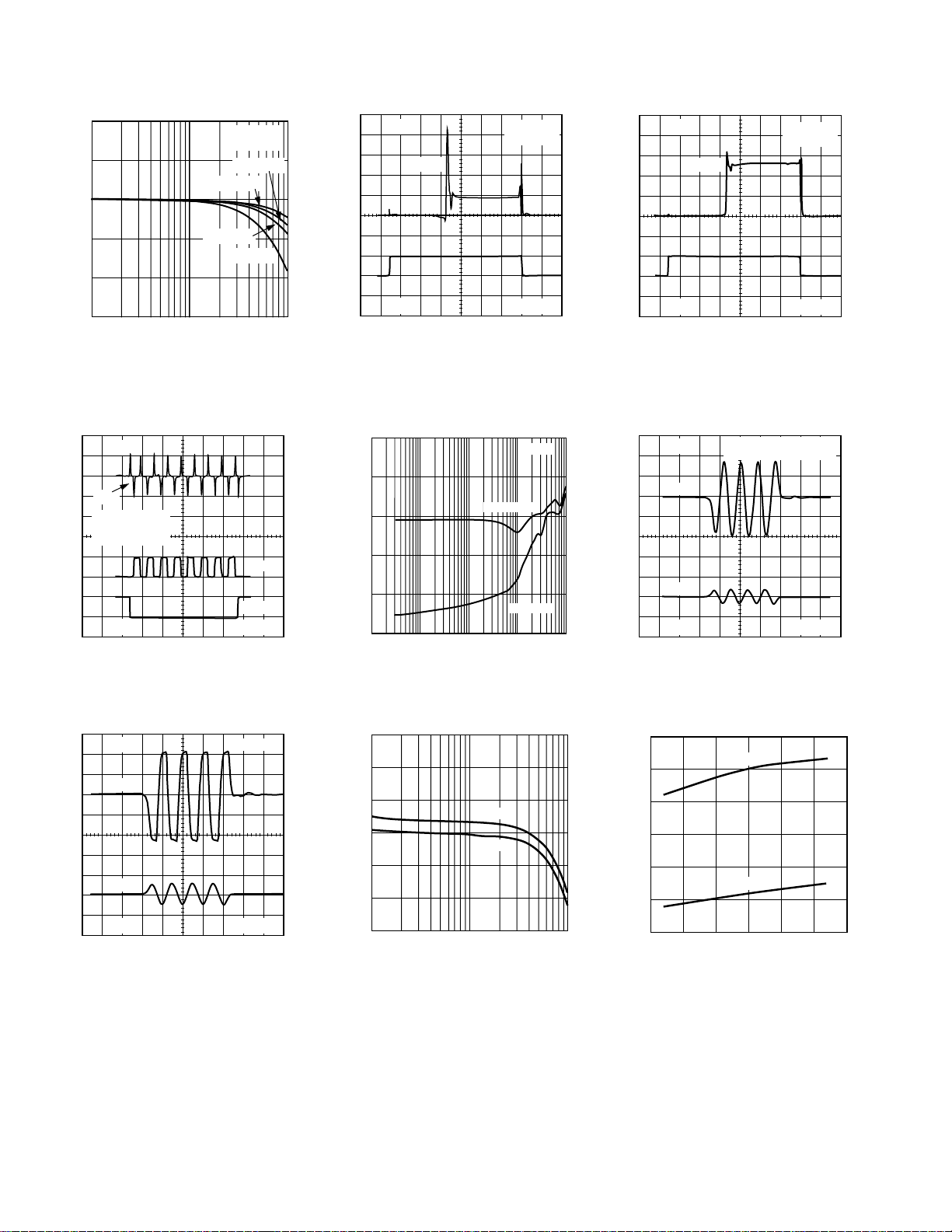
–11–REV. 0
Page 12
AD8321
Differential Input Option 2: Install the Mini-Circuits T1-6TKK81 1:1 transformer in the T1 location of the evaluation
board. Jumpers J1, J2 and J3 should be applied pointing in the
direction of the transformer. Apply an open circuit in the R3
position while J4 is applied connecting the center-tap of the
secondary to ground. A 41 Ω resistor should be used between
each input and ground at R1 and R2. This option will also
result in a 75 Ω differential input termination to the AD8321.
If a 50 Ω single-ended input source is applied to the VIN+/
DIFF IN port, the R1 and R2 values should be 26.7 Ω.
Differential Input Option 3: A differential input may be applied to both VIN– and VIN+ inputs of the evaluation board. In
this example, no transformer is employed. Jumpers J1, J2 and J3
are installed in line with the input signals. Select the differential
input termination configuration of either Option 1 or Option 2.
Apply Option 1 resistor value to R3 for a true differential input
or apply Option 2 values to R1 and R2 to produce ground refer-
enced inputs that are separated in phase by 180°. If the differential input signal source impedance is anything other than 75 Ω
or 50 Ω, calculate the appropriate value according to the equa-
tions below:
For Option 1 Configurations:
Desired Input Impedance = R3储900
For Option 2 and 3 (R1 = R2 = R):
Desired Input Impedance = 2 × (R储450)
DIFF IN
T1
OPTION 1 DIFFERENTIAL INPUT TERMINATION
DIFF IN
T1
OPTION 2 DIFFERENTIAL INPUT TERMINATION
VIN+
VIN–
OPTION 3 DIFFERENTIAL INPUT TERMINATION
R3
R2
R1
R2
R1
AD8321
AD8321
AD8321
Figure 27. Differential Input Termination Options
Controlling the Evaluation Board from a PC
The AD8321-EVAL package comes with the circuit described
by Figure 28 and includes a –2 dB attenuator (reference Rc, Rd
and Re) and the control software allowing the user to program
the gain/attenuation of the AD8321 via a standard printer cable
connected to the parallel port of a PC.
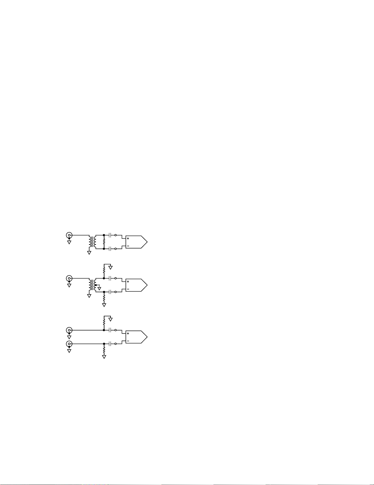
Install Software
To install the “CABDRIVE” software that controls the AD8321EVAL evaluation circuit, close all Windows applications and
select the “SETUP” file located on Disk 1 of the AD8321EVAL software. Follow the on screen instructions (see Figure
29) and insert Disk 2 when prompted to do so. Enter the path
of the directory into which the control software will be installed.
Select the button in the upper left corner to begin the installation of “CABDRIVE” software into the specified directory.
Running the Software
To invoke the control software, select the “Ad8321” icon from
the directory containing the installed software. After invoking
the control software, choose the appropriate printer port from
the display portrayed in Figure 30.
Controlling the Gain/Attenuation of AD8321
The AD8321 control panel has four different functions. The
slide bar controls the gain/attenuation of the AD8321. Adjust
the slider to the gain/attenuation displayed in units of dB. The
additional displays show the selection in units of Volts (output)/
Volts (input), and the corresponding control codes in decimal,
binary and hexadecimal. (See Figure 31.)
“POWER UP” and “POWER DOWN”
The buttons marked “Power Up” and “Power Down” select
the mode of operation of the AD8321. The “Power Up” button
puts the AD8321 in forward transmit mode feeding the conditioned signal to the VOUT port on the evaluation board. Conversely, the “Power Down” button selects the reverse mode
where the forward signal transmission is disabled and the low
noise reverse amplifier actively maintains a 75 Ω back termina-
tion. These features may be selected asynchronously (at any
time). (See the section on Between Burst Transient Reduction
for more specific details.)
Enable Output Switch
An Alpha Industries AS128-73 GaAs 2W Hi Linearity switch is
installed on a standard AD8321-EVAL circuit and is controlled
by the check box on the control panel portrayed in Figure 31.
This feature is intended to remove the output of the AD8321
from the VOUT port prior to using the “Power Up” and
“Power Down” feature described above. This application circuit
may be used to reduce any transients created between bursts to
DOCSIS compliant levels. (See the section on Between Burst
Transient Reduction for more specific details.)
–12–
REV. 0
Page 13

VIN–
J3
82.5V
P1–5
P1–6
P1–2
P1–3
P1– 8
P1–7
R1
TP1
10mF
C1
0.1mF
VCC
SDATA
CLK
DATEN
PD
C15
0.1mF
GND
C
X
V1
V2
R8
1kV
R9
1kV
V
CT
VCC
TP6
TP7
TP8
TP9
TP5
TP4
C6
0.1mF
R6
C16
10mF
C16
1000pF
C17
1000pF
TPc
C12
1000pF
Jb
AD8321
1
AD8321
2
3
TPa
Cc
0.1mF
4
5
6
7
8
9
10
C4
C7
C8
C9
C10
20
19
18
17
16
15
14
13
12
11
C11
C5
Rc Re
C2
0.1mF
Cd
TPd
0.1mF
Rd
Cb
0.1mF
NOTE:
BYPASS CAPACITORS
C4, C5, C7, C8, C9, C10, C11 ARE
0.1mF.
AS128-73
SWb
V1
b
V2
Rb
75V
TP12
TPe
TP13
Vct
Rf
10kV
Ce
0.1mF
TO
DIPLEXER
Figure 28. AD8321-EVAL Schematic of Single-Ended Inverting Input, Upstream PA Driver Solution Using AD8321,
Matching Attenuator and Alpha Industries AS128-73 RF Switch
–13–REV. 0
Page 14
AD8321
EVALUATION BOARD FEATURES AND OPERATION
Figure 29. Evaluation Board Software Installation
Figure 30. Evaluation Board Control Software
–14–
REV. 0
Page 15

AD8321
Figure 31. Screen Display of Windows-Based Control Software
–15–REV. 0
Page 16

AD8321
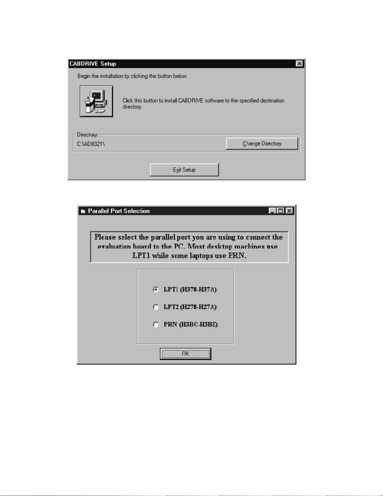
Figure 32. Evaluation Board Silkscreen (Component Side)
–16–
REV. 0
Page 17
AD8321
Figure 33. Evaluation Board Layout (Component Side)
Figure 34. Evaluation Board Layout (Solder Side)
–17–REV. 0
Page 18

AD8321
EVALUATION BOARD BILL OF MATERIALS
AD8321 Evaluation Board Rev. B SINGLE- ENDED INVERTING INPUT March 17, 1999
Qty. Description Vendor Ref Desc.
210µF 16 V. 1350 size tantalum chip capacitor ADS# 4-7-6 C6 & C14
14 0.1 µF 50 V. 1206 size ceramic chip capacitor ADS# 4-5-18 C1–C5, C7–C11, Cb–e
3 1,000 pF 50 V. 1206 size ceramic chip capacitor ADS# 4-5-20 C12, C16 & C17
1 82.5 Ω 1% 1/8 W. 1206 size chip resistor D -K # P 82.5 FCT-ND R1
30 Ω 5% 1/8 W. 1206 size chip resistor ADS# 3-18- 88 R2 & R6, Ca
2 1.00 kΩ 1% 1/8 W. 1206 size chip resistor ADS# 3-18-11 R8 & 9
1 75.0 Ω 1% 1/8 W. 1206 size chip resistor ADS# 3-18-145 Rb
2 649 Ω 1% 1/8 W. 1206 size chip resistor D -K # P 649 FCT-ND Rc & Re
1 10.0 kΩ 1% 1/8 W. 1206 size chip resistor ADS# 3-18-119 Rf
1 17.4 Ω 1% 1/8 W. 1206 size chip resistor D -K # P17.4 FCT-ND Rd
1 Alpha # AS 128-73 GaAs Hi Linearity switch Alpha # AS 128-73 SWb
2 Pink Test Point ADS# 12-18-63 TPc & TPd
1 Blue Test Point [Vct] ADS# 12-18-62 TP14
6 Grey Test Point [Bus lines] ADS# 12-18-64 TP6–TP9, TP12 & TP13
2 Yellow Test Point [INPUTS] ADS# 12-18-32 TP1 & TP2
3 Orange Test Point [OUTPUTS] ADS# 12-18-60 TPa, TPb & TPe
1 Red Test Point [DUT VCC] ADS# 12-18-43 TP4
2 Black Test Point [GND] ADS# 12-18-44 TP5 & TP15
2 2 pin .1 inch ctr. shunt Berg # 65474 - 001 ADS# 11-2-38 J3 & Jb
5 2 pin .1 inch ctr. male Header Berg # 69157 - 102 ADS# 11-2-37 J3, Ja, Jb, Jc, Jd
2 75 Ω right-angle BNC Telegartner # J01003A1949 Comp. Mktg. Services INPUTS, OUTPUT
1 Conn. 36 pin Centronics Right Angle ADS# 12-3-50 P1
4 5-way Metal Binding Post ADS# 12-7-7 DUT VCC, GND, Vct
1 AD8321 AR ADS# AD8321AR D.U.T.
1 AD8321 REV. B Evaluation PC board E.M.C. Evaluation PC board
4 #4 - 40 × 1/4 inch ss panhead machine screw ADS# 30-1-1
4 #4 - 40 × 3/4 inch long aluminum round stand-off ADS# 30-16-3
2 # 2 - 56 × 3/8 inch ss panhead machine screw ADS# 30-1-17 (p1 hardware)
2 # 2 steel flat washer ADS# 30-6-6 (p1 hardware)
2 # 2 steel internal tooth lockwasher ADS# 30-5-2 (p1 hardware)
2 # 2 ss hex. machine nut ADS# 30-7-6 (p1 hardware)
Optional Components J1, J2, J4, R3, Ra, SWa, T1, +VIN+
–18–
REV. 0
Page 19
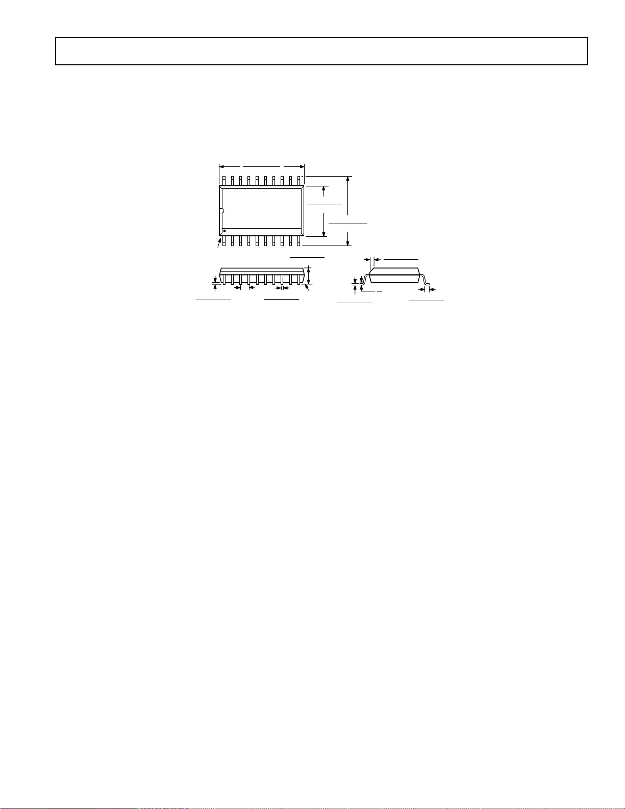
OUTLINE DIMENSIONS
Dimensions shown in inches and (mm).
20-Lead Small Outline Package
(R-20)
0.5118 (13.00)
0.4961 (12.60)
AD8321
20 11
PIN 1
0.0118 (0.30)
0.0040 (0.10)
0.0500
(1.27)
BSC
0.1043 (2.65)
0.0926 (2.35)
0.0192 (0.49)
0.0138 (0.35)
0.2992 (7.60)
0.2914 (7.40)
101
SEATING
PLANE
0.4193 (10.65)
0.3937 (10.00)
0.0125 (0.32)
0.0091 (0.23)
0.0291 (0.74)
0.0098 (0.25)
88
08
C3557–8–4/99
3 458
0.0500 (1.27)
0.0157 (0.40)
PRINTED IN U.S.A.
–19–REV. 0
 Loading...