

Page 1
Serial Digital Controlled
a
FEATURES
8-Bit Serial Gain Control
V/V/LSB Linear Gain Response
36 dB Gain Range
60.20 dB Gain Accuracy
Upper Bandwidth: 150 MHz
22 dBm 1 dB Compression Point (75 V)
Drives Low Distortion Signals into 75 V Load:
–57 dBc SFDR at 42 MHz and 12 dBm Out
–46 dBc SFDR at 42 MHz and 18 dBm Out
Single Supply Operation from 5 V to 12 V
Maintains 75 V Output Impedance
Power-Up and Power-Down Condition
Supports SPI Input Control Standard
APPLICATIONS
Coaxial Cable Driver
HFC Cable Telephony Systems
HFC High Speed Data Modems
Interactive Set-Top Boxes
PC Plug-In Modems
Interfaces with AD9853 I
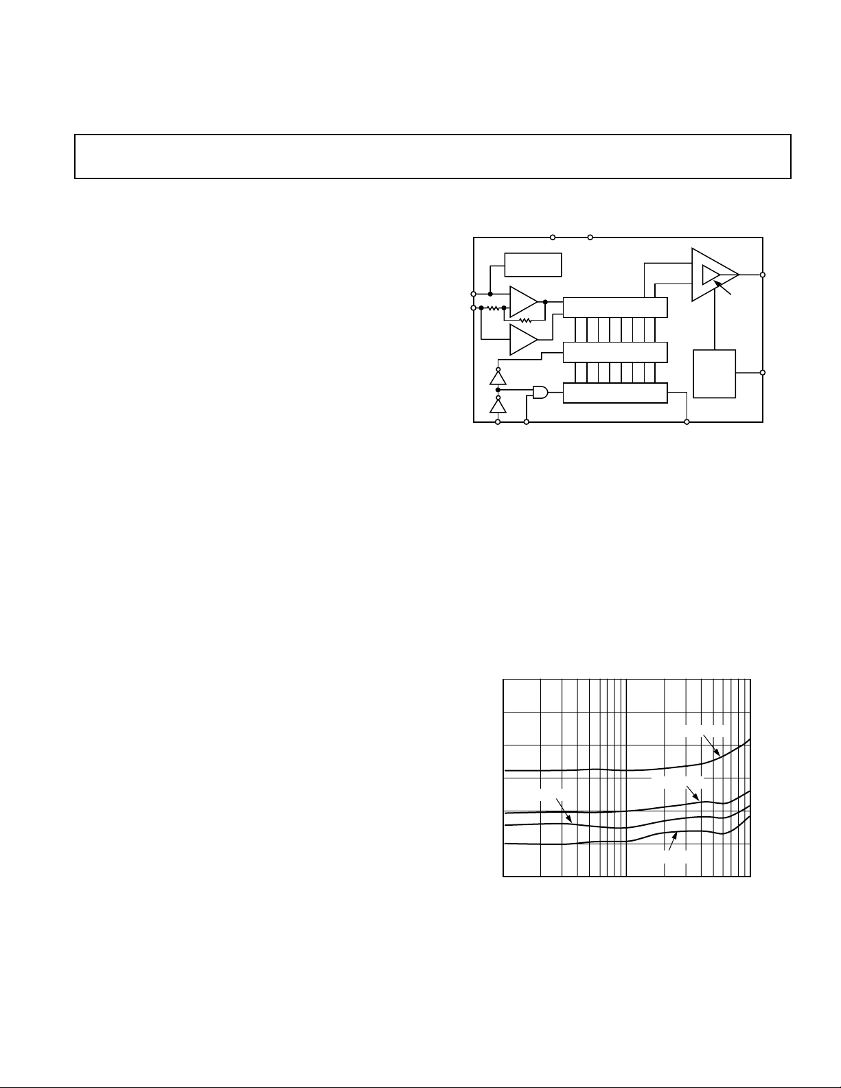
High Performance Digitally Controlled Variable Gain
Block
2
C Controlled Digital Modulator
Variable Gain Line Driver
FUNCTIONAL BLOCK DIAGRAM
GNDVCC
REFERENCE
VREF
VIN
INV.
BUF.
DATEN CLK SDATA
AD8320
ATTENUATOR CORE
DATA LATCH
DATA SHIFT REGISTER
AD8320
PWR AMP
REVERSE
AMP
POWER-
DOWN/
SWITCH
INTER.
VOUT
PD
DESCRIPTION
The AD8320 is a digitally controlled variable gain amplifier
optimized for coaxial line driving applications. An 8-bit serial
word determines the desired output gain over a 36 dB range
(256 gain levels). The AD8320 provides linear gain response.
The AD8320 is made up of a digitally controlled variable attenuator of 0 dB to –36 dB, which is preceded by a low noise,
fixed gain buffer and followed by a low distortion high power
amplifier. The AD8320 has a 220 Ω input impedance and accepts a single-ended input signal with a specified analog input
level of up to 0.310 V p-p. The output is specified for driving a
75 Ω load, such as coaxial cable, although the AD8320 is capable of driving other loads. Distortion performance of –57 dBc
is achieved with an output level up to 12 dBm (3.1 V p-p) at
42 M H z, while –46 dBc distortion is achieved with an output
level up to 18 dBm (6.2 V p-p).
A key performance and cost advantage of the AD8320 results
from the ability to maintain a constant 75 Ω output impedance
during power-up and power-down conditions. This eliminates
the need for external 75 Ω back-termination, resulting in twice
the effective output voltage when compared to a standard operational amplifier. Additionally, the on-chip 75Ω termination
REV. 0
Information furnished by Analog Devices is believed to be accurate and
reliable. However, no responsibility is assumed by Analog Devices for its
use, nor for any infringements of patents or other rights of third parties
which may result from its use. No license is granted by implication or
otherwise under any patent or patent rights of Analog Devices.
results in low glitch output during power-down and power-up
transitions, eliminating the need for an external switch.
The AD8320 is packaged in a 20-lead SOIC and operates from
a single +5 V through +12 V supply and has an operational
temperature range of –40°C to +85°C.
220
230
PO = 18dBm
240
250
PO = 8dBm
260
DISTORTION – dBc
270
280
1
FREQUENCY – MHz
PO = 12dBm
PO = 4dBm
10 100
Figure 1. Worst Harmonic Distortion vs. Frequency for
Various Output Levels at V
One Technology Way, P.O. Box 9106, Norwood, MA 02062-9106, U.S.A.
Tel: 781/329-4700 World Wide Web Site: http://www.analog.com
Fax: 781/326-8703 © Analog Devices, Inc., 1998
= 12 V
CC
Page 2

(@ VCC = 12 V, TA = +258C, VIN = 0.310 V p-p, RL = 75 V, RS = 75 V unless
AD8320–SPECIFICA TIONS
otherwise noted)
Parameter Conditions Min Typ Max Units
INPUT CHARACTERISTICS
Full-Scale Input Voltage Max Gain, P
Max Gain, P
= 18 dBm, VCC = 12 V 0.310 V p-p
OUT
= 12 dBm, VCC = 5 V 0.155 V p-p
OUT
Input Resistance 220 Ω
Input Capacitance 2.0 pF
GAIN CONTROL INTERFACE
Gain Range 36 dB
Full Scale (Max) Gain 26 (20) dB (V/V)
Gain Offset (Min) Gain –10.0 (0.316) dB (V/V)
Gain Scaling Factor 0.077 V/V/LSB
OUTPUT CHARACTERISTICS
Bandwidth (–3 dB) All Gain Codes 150 MHz
Bandwidth Roll-Off F = 65 MHz 0.7 dB
Bandwidth Peaking F = 65 MHz 0 dB
Output Offset Voltage All Gain Codes ± 40 mV
Output Offset Drift Full Temperature Range ±0.25 mV/°C
Output Noise Spectral Density Max. Gain, Frequency = 10 MHz 73 nV/√Hz
Min. Gain, Frequency = 10 MHz 53 nV/√ Hz
PD = 0, Frequency = 10 MHz 4.5 nV/√Hz
1 dB Compression Point V
= 12 V 22.5 dBm
CC
V
= 5 V 16 dBm
CC
Output Impedance Power Up and Power Down 65 75 85 Ω
Overload Recovery Max Gain, VIN = 500 mV p-p 40 ns
OVERALL PERFORMANCE
Worst Harmonic Distortion F = 42 MHz, P
F = 42 MHz, P
F = 42 MHz, P
F = 65 MHz, P
F = 65 MHz, P
F = 65 MHz, P
3rd Order Intercept F = 42 MHz, P
F = 42 MHz, P
F = 65 MHz, P
F = 65 MHz, P
= 12 dBm, VCC = 12 V –57.0 –52.0 dBc
OUT
= 12 dBm, VCC = 5 V –43.0 –39.0 dBc
OUT
= 18 dBm, VCC = 12 V –46.0 –42.0 dBc
OUT
= 12 dBm, VCC = 12 V –57.0 –52.0 dBc
OUT
= 12 dBm, VCC = 5 V –42.5 –39.0 dBc
OUT
= 18 dBm, VCC = 12 V –43.0 –40.0 dBc
OUT
= 18 dBm, VCC = 12 V 34 dBm
OUT
= 12 dBm, VCC = 5 V 32 dBm
OUT
= 18 dBm, VCC = 12 V 32.5 dBm
OUT
= 12 dBm, VCC = 5 V 28.5 dBm
OUT
Full-Scale (Max Gain) Accuracy F = 10 MHz ± 0.1 dB
Gain Offset (Min Gain) Accuracy F = 10 MHz ± 0.2 dB
Gain Accuracy F = 10 MHz, All Gain Codes –0.75 ±0.2 0.75 dB
Gain Drift Full Temperature Range ±0.5 mdB/°C
Gain Variation w/Supply V
= +5 V to 12 V 35 mdB/V
CC
Output Settling to 1 mV
Gain Change @ T
= 1 Min to Max Gain, VIN = 0.31 V p-p 30 ns
DATEN
Input Change Max Gain, VIN = 0 V to 0.31 V p-p 25 ns
POWER CONTROL
Power-Down Settling Time to 1 mV Max Gain, V
Power-Up Settling Time to 1 mV Max Gain, V
Power-Down Pedestal Offset Max Gain, V
= 0 45 ns
IN
= 0 65 ns
IN
= 0 ±30 mV
IN
Spectral Output Leakage F (PD) = 400 Hz @ 15% Duty Cycle –70 dBm
5 MHz ≤ F ≤ 65 MHz
Maximum Reverse Power PD = 0 5 dBm
POWER SUPPLY
Specified Operating Range +5 +12 V
Quiescent Current PD = 1, V
Power Down PD = 0, V
Power Up, V
= +12 V PD = 1, VCC = +12 V 97 105 mA
CC
= +5 V 80 85 mA
CC
= +5 V 25 30 mA
CC
Power Down, VCC =+12 V PD = 0, VCC = +12 V 32 37 mA
–2–
REV. 0
Page 3
AD8320
LOGIC INPUTS (TTL/CMOS Logic)
(DATEN, CLK, SDATA, 5 V ≤ VCC ≤ 12 V; Full Temperature Range)
Parameter Min Typ Max Units
Logic “1” Voltage 2.1 5.0 V
Logic “0” Voltage 0 0.8 V
Logic “1” Current (V
Logic “0” Current (V
Logic “1” Current (V
Logic “0” Current (V
TIMING REQUIREMENTS
= 5 V) CLK, SDATA, DATEN 020nA
INH
= 0 V) CLK, SDATA, DATEN –450 –75 nA
INL
= 5 V) PD 0 190 µA
INH
= 0 V) PD –320 –70 µA
INL
(Full Temperature Range, VCC Supply Range, TR = TF = 4 ns, F
= 8 MHz unless otherwise noted.)
CLK
Parameter Min Typ Max Units
Clock Pulse Width (T
Clock Period (T
C
Setup Time SDATA vs. Clock (T
Setup Time DATEN vs. Clock (T
Hold Time SDATA vs. Clock (T
Hold Time DATEN vs. Clock (T
) 12.0 ns
WH
) 32.0 ns
) 6.5 ns
DS
) 17.0 ns
ES
) 5.0 ns
DH
) 3.0 ns
EH
Input Rise and Fall Times, SDATA, DATEN, Clock (TR, TF)10ns
T
DS
SDATA
CLK
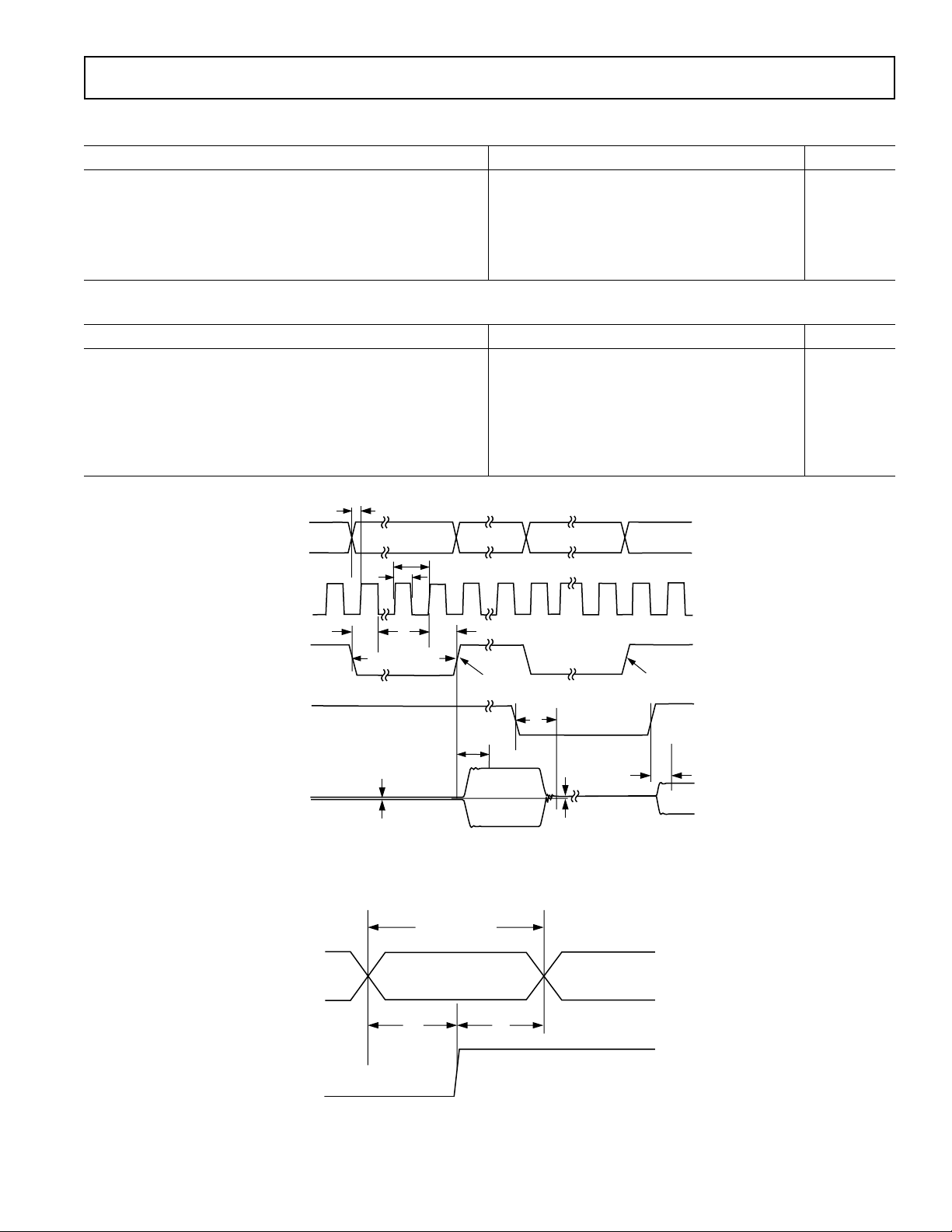
VALID DATA WORD G1
MSB. . . .LSB
T
C
T
WH
VALID DATA WORD G2
DATEN
PD
ANALOG
OUTPUT
T
ES
8 CLOCK CYCLES
SIGNAL AMPLITUDE (p-p)
T
EH
GAIN TRANSFER (G1)
T
Figure 2. Serial Interface Timing
VALID DATA BIT
MSB
T
CLK
MSB-1 MSB-2
DS
GAIN TRANSFER (G2)
T
OFF
GS
T
ON
PEDESTAL
T
DH
Figure 3.
–3–REV. 0
Page 4
AD8320
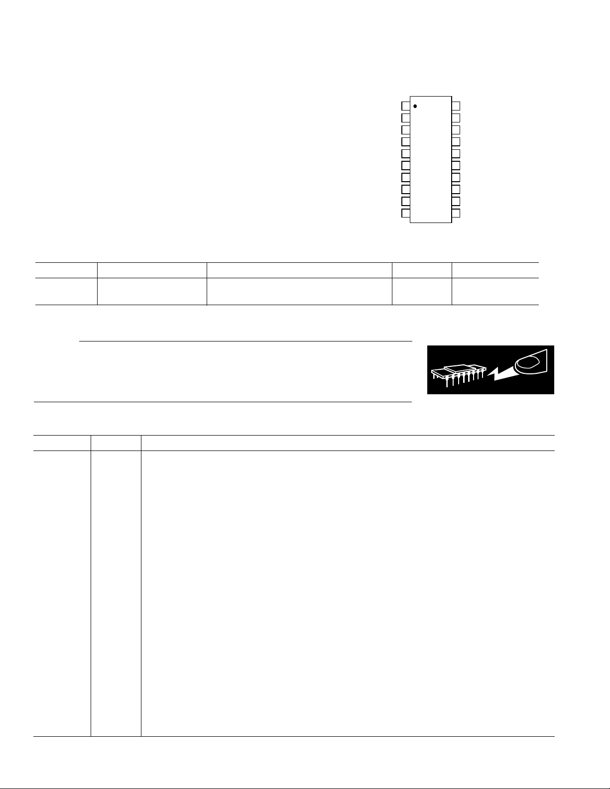
TOP VIEW
(Not to Scale)
20
19
18
17
16
15
14
13
12
11
1
2
3
4
5
6
7
8
9
10
AD8320
VOUT
VCC
VCC
CLK
DATEN
GND
VCC
PD
VOCM
GND
GND
VIN
VREF
VCC
BYP
GND
GND
SDATA
VCC
GND
ABSOLUTE MAXIMUM RATINGS*
Supply Voltage +V
S
PIN CONFIGURATION
Pins 7, 8, 9, 17, 20 . . . . . . . . . . . . . . . . . . . –0.8 V to +13 V
Input Voltages
Pins 19 . . . . . . . . . . . . . . . . . . . . . . . . . . . . . . . . . . . . . ±3 V
Pins 1, 2, 3, 6 . . . . . . . . . . . . . . . . . . . . . . . . –0.8 V to +5 V
Internal Power Dissipation
Small Outline (RP) . . . . . . . . . . . . . . . . . . . . . . . . . . 1.3 W
Operating Temperature Range . . . . . . . . . . . –40°C to +85°C
Storage Temperature Range . . . . . . . . . . . . –65°C to +150°C
Lead Temperature, Soldering 60 seconds . . . . . . . . . . +300°C
*Stresses above those listed under Absolute Maximum Ratings may cause perma-
nent damage to the device. This is a stress rating only; functional operation of the
device at these or any other conditions above those indicated in the operational
section of this specification is not implied. Exposure to absolute maximum rating
conditions for extended periods may affect device reliability.
ORDERING GUIDE
Model Temperature Range Package Description u
JA
Package Option
AD8320ARP –40°C to +85°C 20-Lead Thermally Enhanced Power SOIC* 53°C/W RP-20
AD8320-EB Evaluation Board
*Shipped in tubes (38 pieces/tube) and dry packed per J-STD-020.
CAUTION
ESD (electrostatic discharge) sensitive device. Electrostatic charges as high as 4000 V readily
accumulate on the human body and test equipment and can discharge without detection.
WARNING!
Although the AD8320 features proprietary ESD protection circuitry, permanent damage may
occur on devices subjected to high energy electrostatic discharges. Therefore, proper ESD
precautions are recommended to avoid performance degradation or loss of functionality.
ESD SENSITIVE DEVICE
PIN FUNCTION DESCRIPTIONS
Pin Function Description
1 SDATA Serial Data Input. This digital input allows for an 8-bit serial (gain) word to be loaded into the internal
register with the MSB (most significant bit) first.
2 CLK Clock Input. The clock port controls the serial attenuator data transfer rate to the 8-bit master-slave
register. A Logic 0 to 1 transition latches the data bit and a 1 to 0 transfers the data bit to the slave.
This requires the input serial data word to be valid at or before this clock transition.
3 DATEN Data Enable Low Input. This port controls the 8-bit parallel data latch and shift register. A Logic 0 to 1
transition transfers the latched data to the attenuator core (updates the gain) and simultaneously inhibits serial data transfer into the register. A 1 to 0 transition inhibits the data latch (holds the previous
gain state) and simultaneously enables the register for serial data load.
4, 11, 12,
13, 15, 16 GND Common External Ground Reference.
5 VOCM VCC/2 Reference Pin. A dc output reference level that is equal to 1/2 of the supply voltage (VCC).
This port should be externally ac decoupled (0.1µF cap).
6 PD Power-Down Low Logic Input. A Logic 0 powers down (shuts off) the power amplifier disabling the
output signal and enabling the reverse amplifier. A Logic 1 enables the output power amplifier and
disables the reverse amplifier.
7, 8, 9, 17, 20 VCC Common Positive External Supply Voltage.
10 VOUT Output Signal Port. DC biased to approximately VCC/2.
14 BYP Internal Bypass. This pin must be externally ac decoupled (0.1 µF cap).
18 VREF Input Reference Voltage (typically 1.9 V at 27°C). This port should be externally ac decoupled
19 VIN Analog Voltage Input Signal Port. DC biased to VREF voltage.
(0.1 µF cap).
–4–
REV. 0
Page 5
T ypical Performance Characteristics–AD8320
GAIN CONTROL – Decimal
GAIN ERROR – dB
0.45
0
0
20.30
20.15
20.45
64 128 192 256
0.15
F = 10MHz
T = +258C
VCC = 5V
VCC = 12V
0.30
FREQUENCY – Hz
220
100k 1G1M 10M 100M
290
VCC = 12V, PIN = 28dBm
FEEDTHROUGH – dB
VCC = 5V, PIN = 214dBm
MAX GAIN
PD = 0V
230
240
250
260
270
280
2100
0.3
VCC = 12V
F = 10MHz
0.2
0.1
0
20.1
GAIN ERROR – dB
20.2
20.3
T = 2408C
0
GAIN CONTROL – Decimal
T = +858C
64 128 192
T = +258C
256
Figure 4. Gain Error vs. Gain Control
at Various Temperatures
30
20
10
0
GAIN – dB
210
255D
170D
85D
01D
00D
VCC = 5V
0.6
0.3
0
20.3
GAIN ERROR – dB
20.6
20.9
21.2
0
GAIN CONTROL – Decimal
64 128 192 256
VCC = 12V
T = +258C
10MHz
42MHz
65MHz
Figure 5. Gain Error vs. Gain Control
at Various Frequencies
30
20
10
GAIN – dB
0
210
255D
170D
85D
01D
00D
VCC = 12V
Figure 6. Gain Error vs. Gain Control
at Different Supply Voltages
220
100k 1G1M 10M 100M
Figure 7. AC Response
80
F = 10MHz
75
V
CC
70
65
60
55
50
OUTPUT NOISE – nV/!Hz
45
40
064
Figure 10. Output Referred Noise vs.
Gain Control at Various Temperatures
REV. 0
FREQUENCY – Hz
= 12V
+858C
128 192
GAIN CONTROL – Decimal
+258C
2408C
256
220
100k 1G1M 10M 100M
FREQUENCY – Hz
Figure 8. AC Response
80
F = 10MHz
75
70
65
60
55
50
OUTPUT NOISE – nV/!Hz
45
40
064
VCC = 12V
VCC = 5V
GAIN CONTROL – Decimal
128 192
256
Figure 11. Output Referred Noise vs.
Gain Control at Different Supply
Voltages
–5–
Figure 9. Input Signal Feedthrough
vs. Frequency
90
80
70
MAX GAIN, VCC = 5V
60
50
OUTPUT NOISE – nV/!Hz
40
30
100k
MAX GAIN, VCC = 12V
MIN GAIN, VCC = 12V
MIN GAIN, VCC = 5V
1M
FREQUENCY – Hz
10M 100M
Figure 12. Output Referred Noise vs.
Frequency
Page 6
AD8320
230
VCC = 12V
240
F = 42MHz, PO = 18dBm
250
260
270
DISTORTION – dBc
280
F = 65MHz, PO = 12dBm
290
0 64 128 192 256
F = 65MHz, PO = 18dBm
F = 42MHz, PO = 12dBm
GAIN CONTROL – Decimal
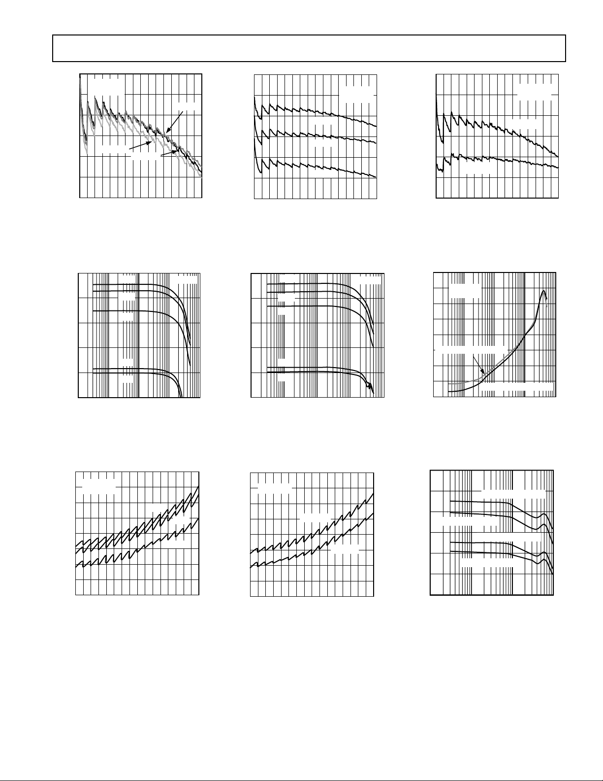
Figure 13. Worst Harmonic Distortion vs. Gain Control
220
230
240
250
PO = 8dBm
260
DISTORTION – dBc
270
280
1 10 100
PO = 18dBm
PO = 12dBm
PO = 4dBm
FREQUENCY – MHz
Figure 16. Worst Harmonic Distortion vs. Frequency for Various Output
Levels at VCC = 10 V
220
230
240
250
260
DISTORTION – dBc
270
280
1 10 100
PO = 12dBm
PO = 10dBm
PO = 8dBm
PO = 4dBm
FREQUENCY – MHz
Figure 14. Worst Harmonic Distortion vs. Frequency for Various Output
Levels at VCC = 5 V
220
230
240
250
PO = 8dBm
260
DISTORTION – dBc
270
280
1
FREQUENCY – MHz
PO = 18dBm
PO = 12dBm
PO = 4dBm
10 100
Figure 17. Worst Harmonic Distortion vs. Frequency for Various Output
Levels at VCC = 12 V
220
230
240
250
260
DISTORTION – dBc
270
280
1 10 100
PO = 10dBm
PO = 8dBm
FREQUENCY – MHz
PO = 12dBm
PO = 4dBm
Figure 15. Worst Harmonic Distortion vs. Frequency for Various Output
Levels at VCC = 6 V
40
30
20
PERCENTAGE
10
0
247
HARMONIC DISTORTION – dBc
246 245 244 243
VCC = 12V
= 18dBm
P
O
F = 42MHz
N = 30
Figure 18. Distribution of Worst Harmonic Distortion
40
30
20
PERCENTAGE
10
0
245
HARMONIC DISTORTION 2 dBc
244 243 242 241
VCC = 12V
P
= 18dBm
O
F = 65MHz
N = 30
Figure 19. Distribution of Worst Harmonic Distortion
20
VCC = 12V
P
= 12dBm
O
15
10
PERCENTAGE
5
0
259
HARMONIC DISTORTION 2 dBc
258 257 256 255
F = 42MHz
N = 30
Figure 20. Distribution of Worst Harmonic Distortion
–6–
30.0
22.5
15.0
PERCENTAGE
7.5
0
244
HARMONIC DISTORTION 2 dBc
243 242 241 240
VCC = 5V
P
= 12dBm
O
F = 65MHz
N = 30
Figure 21. Distribution of Worst Harmonic Distortion
REV. 0
Page 7

AD8320
FREQUENCY – MHz
45
1 10 100
35
30
3RD ORDER INTERCEPT – dBm
40
25
VCC = 12V
PO = 12dBm
20
PO = 18dBm
235
F = 42MHz, VCC = 5V, PO = 12dBm
240
245
250
F = 65MHz
V
= 12V
250
DISTORTION 2 dBc
255
260
265
250 225
F = 42MHz
V
= 12V
CC
= 18dBm
P
O
F = 65MHz, VCC = 12V, PO = 12dBm
075
TEMPERATURE 2 8C
CC
250
= 18dBm
P
O
25 50 100
Figure 22. Harmonic Distortion vs.
Temperature
VCC = 12V
= 310mV p-p
V
IN
MIN GAIN
F = 10MHz
20
PO = 18dBm
MAX GAIN
VCC = 12V
42.041.2 42.4 42.8
–20
– dBm
OUT
P
–40
–60
–80
0
41.6
FREQUENCY – MHz
Figure 23. Two-Tone Intermodulation Distortion
VCC = 12V
= 310mV p-p
V
IN
MAX GAIN
F = 10MHz
Figure 24. Third Order Intercept vs.
Frequency
30
27
24
21
GAIN – dB
CL = 22pF
CL = 100pF
VCC = 5V
MAX GAIN
CL = 0pF
CL = 150pF
FREQUENCY – Hz
20mV
12.5nsec
Figure 25. Transient Response
12.5nsec1.2V
Figure 26. Transient Response
18
15
100k 1G1M 10M 100M
Figure 27. AC Response for Various
Capacitive Loads
30
VCC = 5V
MAX GAIN
F = 1MHz
CL = 0pF
OUTPUT VOLTAGE – Volts
500mV
TIME – Seconds
CL = 22pF
CL = 100pF
CL = 150pF
5nsec
Figure 28. Transient Response for
Various Capacitive Loads
27
24
21
GAIN – dB
18
15
100k 1G1M 10M 100M
CL = 22pF
CL = 100pF
CL = 150pF
FREQUENCY – Hz
Figure 29. AC Response for Various
Capacitive Loads
VCC = 12V
MAX GAIN
CL = 0pF
VCC = 12V
MAX GAIN
F = 1MHz
CL = 0pF
1V
CL = 22pF
CL = 100pF
CL = 150pF
5nsec
Figure 30. Transient Response for
Various Capacitive Loads
–7–REV. 0
Page 8

AD8320
100mV
V
OUT
5V
5V
VCC = 12V
MAX GAIN
V
= 0V p-p
IN
PD
75nsec
Figure 31. Power-Up/Power-Down
Glitch
2.50V
V
OUT
V
IN
5V1V
VCC = 12V
F = 40MHz
MAX GAIN
20nsec
Figure 34. Overload Recovery
5mV
V
OUT
5V
5V
VCC = 12V
MAX GAIN
V
= 0V p-p
IN
CLK
DATEN
250nsec
Figure 32. Clock Feedthrough
2.00V
V
OUT
V
IN
250mV
VCC = 12V, F = 40MHz
MAX GAIN
20nsec
Figure 35. Output Settling Time Due
to Input Change
1.25V
V
OUT
V
IN
5V500mV
VCC = 5V
F = 40MHz
MAX GAIN
20nsec
Figure 33. Overload Recovery
2.50V
V
5V
OUT
DATEN
VCC = 12V, F = 40MHz
MIN TO MAX GAIN
V
= .310V p-p
IN
20nsec
Figure 36. Output Settling Time Due
to Gain Change
80
70
60
50
INPUT IMPEDANCE – V
40
100k 1G1M 10M 100M
FREQUENCY – Hz
VCC = 5V
= 115V
R
T
Figure 37. Input Impedance vs.
Frequency
90
VCC = 5V, PD = 0
80
70
VCC = 12V, PD = 0
60
OUTPUT IMPEDANCE – V
50
100k 1M 10M 100M
VCC = 5V, PD = 1
VCC = 12V, PD = 1
FREQUENCY – Hz
Figure 38. Output Impedance vs.
Frequency
120
0
–50 –25
VCC = 12V, PD = 1
VCC = 5V, PD = 1
VCC = 12V, PD = 0
VCC = 5V, PD = 0
0 25 50 75 100
TEMPERATURE – 8C
100
80
60
40
SUPPLY CURRENT – mA
20
Figure 39. Supply Current vs.
Temperature
–8–
REV. 0
Page 9

–16
GAIN – Code – Decimal
–8
0 25632
GAIN – dB
64 96 128 160 192 224
24
8
0
32
16
AV = 20 3 LOG10 (0.316 + 0.077 3 CODE)
OPERATIONAL DESCRIPTION
The AD8320 is a digitally controlled variable gain power amplifier that is optimized for driving 75 Ω cable. A multifunctional
bipolar device on single silicon, it incorporates all the analog
features necessary to accommodate reverse path (upstream) high
speed (5 MHz to 65 MHz) cable data modem and cable telephony requirements. The AD8320 has an overall gain range of
36 dB (–10 dB to 26 dB) and is capable of greater than 100MHz
of operation at output signal levels exceeding 18 dBm. Overall,
when considering the device’s wide gain range, low distortion,
wide bandwidth and variable load drive, the device can be used
in many variable gain block applications.
The digitally programmable gain is controlled by the three wire
“SPI” compatible inputs. These inputs are called SDATA
(serial data input port), DATEN (data enable low input port)
and CLK (clock input port). See Pin Function Descriptions and
Functional Block diagram. The AD8320 is programmed by an
8-bit “attenuator” word. These eight bits determine the 256
programmable gain settings. See attenuator core description
below. The gain is linear in V/V/LSB and can be described by
the following equation:
A
= 0.316 + 0.077 × Code (RL = 75 Ω)
V
where code is the decimal equivalent of the 8-bit word. For example, if all 8 bits are at a logic “1,” the decimal equivalent is
255 and A
equals 19.95 V/V or 26 dB. The gain scaling factor
V
is 0.077 V/V/LSB, with an offset of 0.316 V/V (–10.0dB). Figure 40 shows the linear gain versus decimal code and Figure 41
shows the gain in dB versus decimal code. Note the nonlinearity that results when viewed in dB versus code. The dB step
size increases as the attenuation increases (i.e., gain decreases)
and reaches a maximum step size of approximately 1.9dB (gain
change between 01 and 00 decimal).
22
20
18
AV = 0.316 + 0.077 3 CODE
16
14
12
10
8
GAIN – V/V
6
4
2
0
–2
0 25632
64 96 128 160 192 224
POWER-UP
POWER-DOWN
GAIN – Code – Decimal
Figure 40. Linear Gain vs. Gain Control
The AD8320 is composed of three analog functions in the powerup or forward mode (Figure 42). The input inverter/buffer
amplifier provides single-ended to differential output conversion. The output signals are nominally 180 degrees out of phase
and equal in amplitude with a differential voltage gain of 2 (6 dB).
Maintaining close to 180 degrees and equal amplitude is required for proper gain accuracy of the attenuator core over the
specified operating frequency. The input buffer/inverter also
provides equal dc voltages to the core inputs via the internal
reference. This is required to ensure proper core linearity over
the full specified power supply range (5 V to 12V).
–9–REV. 0
AD8320
Figure 41. Log Gain vs. Gain Control
The attenuator core can be viewed as eight binarily weighted
(differential in–differential out) transconductance (gm) stages
with the “in phase” current outputs of all eight stages connected
in parallel to their respective differential load resistors (not
shown). The core differential output signals are also 180 degrees
out of phase and equal in amplitude. The input stages are likewise parallel, connected to the inverting input amplifier and
buffer outputs as shown. Nine bits plus of accuracy is achieved
for all gain settings over the specified frequency, supply voltage
and temperature range. The actual total core GM × RL attenuation is determined by which combination of binarily weighted
gm stages are selected by the data latch. With 8 bits, 256 levels
of attenuation can be programmed. This results in a 36dB
attenuation range (0 dB to –36 dB). See gain equation above.
GNDVCC
REFERENCE
VREF
VIN
INV.
BUF.
DATEN CLK SDATA
AD8320
ATTENUATOR CORE
DATA LATCH
DATA SHIFT REGISTER
Figure 42. Functional Block Diagram
To update the AD8320 gain, the following digital load sequence
is required. The attenuation setting is determined by the 8-bit
word in the data latch. This 8-bit word is serially loaded (MSB
first) into the shift register at each rising edge of the clock. See
Figure 43. During this data load time (T), DATEN is low and
the data latch is latched holding the previous (T– 1) data word
keeping the attenuation level unchanged. After eight clock
cycles the new data word is fully loaded and DATEN is
switched high. This enables the data latch (becomes transparent) and the loaded register data is passed to the attenuator with
the updated gain value. Also at this DATEN transition, the
internal clock is disabled, thus inhibiting new serial input data.
PWR AMP
REVERSE
POWER–
DOWN
SWITCH
INTER.
VOUT
AMP
PD
Page 10

AD8320
SDATA
CLK
T
DS
VALID DATA WORD G1
MSB. . . .LSB
T
C
T
WH
VALID DATA WORD G2
DATEN
PD
ANALOG
OUTPUT
T
ES
8 CLOCK CYCLES
SIGNAL AMPLITUDE (p-p)
T
EH
GAIN TRANSFER (G1)
T
GS
Figure 43. Serial Interface Timing
The power amplifier has two basic modes of operation; forward
or power-up mode and reverse or power-down mode. In the
power-up mode (PD = 1), the power amplifier stage is enabled
and the differential output core signal is amplified by 20dB.
With a core attenuation range of 0 dB to –36 dB and 6dB of
input gain, the overall AD8320 gain range is 26 dB to –10dB.
In this mode, the single-ended output signal maintains a dc
level of VCC/2. This dc output level provides for optimum large
signal linearity and allows for dc coupling the output if necessary. The output stage is unique in that it maintains a dynamic
output impedance of 75 Ω. This allows for a direct 75 Ω cable
connection and results in 6 dB of added load power versus using
a series 75 Ω back-termination resistor as required with traditional low output impedance amplifiers. The power amplifier
will also drive lower or higher output loads, although the device’s
gain (not gain range) will change accordingly (see Applications
section).
In the power-down mode (PD = 0), the power amplifier is turned
off and a “reverse” amplifier (the inner triangle in Figure 42) is
enabled. During this 1 to 0 transition, the output power amplifier’s
input stage is also disabled, resulting in no forward output signal
(S21 is 0), although the attenuator core and input amplifier/
buffer signals are not affected (S11 ≈ 0). The function of the
reverse amplifier is to maintain 75 Ω and VCC/2 at the output
port (VOUT) during power-down. This is required to minimize
line reflections (S22 ≈ 0) and ensures proper filter operation for
any forward mode device sharing the same bus (i.e., in a multiplexed configuration). (See Applications section.) In the time
domain, as PD switches states, a transitional glitch and pedestal
offset results. (See Figures 31 and 43.) The powered down
supply current drops to 32 mA versus 97 mA (V
= 12 V) in
CC
power-up mode.
Generally, using the power-down low input (PD) for switching
allows for multiple devices to be multiplexed via splitters (N-1
off, 1 on) and reduces overall total power consumption as required for cable data applications. For cable telephony, the
power-down current generally needs to be much lower during
GAIN TRANSFER (G2)
T
OFF
T
ON
PEDESTAL
what is referred to as sleep and standby modes, and VCC supply
switching via PFETS or equivalent, as described in the applications section, would be required.
APPLICATIONS
The AD8320 is primarily intended to be used as the return path
(also called upstream path) line driver in cable modem and
cable telephony applications. Data to be transmitted is modulated in either QPSK or QAM format. This is done either in
DSP or by a dedicated QPSK/QAM modulator such as the
AD9853.
The amplifier receives its input signal either from the dedicated
QPSK/QAM modulator or from a DAC. In both cases, the
signal must be low-pass filtered before being applied to the line
driving amplifier.
CENTRAL
OFFICE
75V
AD9853
TO MODEM
RECEIVE
CIRCUITRY
7TH ORDER
ELLIPTIC
LOW PASS
FILTER
SUBSCRIBER
DIPLEXER
AD8320
Figure 44. Block Diagram of Cable Modem’s Upstream
Driver Section
The amplifier drives the line through a diplexer. The insertion
loss of a diplexer is typically –3 dB. As a result, the line driver
must deliver a power level roughly 3 dB greater than required by
the applicable cable modem standard so that diplexer losses are
canceled out.
Because the distance to the central office varies from subscriber
to subscriber, signals from different subscribers will be attenuated by differing amounts. As a result, the line driver is required
to vary its gain so that all signals arriving at the central office
have the same amplitude.
–10–
REV. 0
Page 11

AD8320
Basic Connection
Figure 45 shows the basic schematic for operating the AD8320.
Because the amplifier operates from a single supply, the input
signal must be ac-coupled using a 0.1 µF capacitor. The input
pin has a bias level of about 1.9 V. This bias level is available on
the VREF pin (Pin 18) and can be used to externally bias signals
if dc-coupling is desired. Under all conditions, a 0.1 µF decoupling
capacitor must be connected to the VREF pin. If the VREF voltage is to be used externally, it should be buffered first.
The VIN pin of the AD8320 (Pin 19) has an input impedance
of 220 Ω. Typically, in video applications, 75 Ω termination is
favored. As a result, an external shunt resistance (R1) to ground
of 115 Ω is required to create an overall input impedance of
75 Ω. If 50 Ω termination is required, a 64.9Ω shunt resistor
should be used. Note, to avoid dc loading of the VIN pin, the
ac-coupling capacitor should be placed between the input pin
and the shunt resistor as shown in Figure 45.
On the output side, the VOUT pin also has a dc bias level. In
this case the bias level is midway between the supply voltage and
ground. The output signal must therefore be ac-coupled before
being applied to the load. The dc bias voltage is available on the
VOCM pin (Pin 5) and can be used in dc-coupled applications.
This node must be decoupled to ground using a 0.1 µF capaci-
tor. If the VOCM voltage is to be used externally, it should be
buffered.
Since the AD8320 has a dynamic output impedance of 75Ω, no
external back termination resistor is required. If the output
signal is being evaluated on 50 Ω test equipment such as a spectrum analyzer, a 75 Ω to 50 Ω adapter (commonly called a pad)
should be used to maintain a properly matched circuit.
Varying the Gain
The gain of the AD8320 can be varied over a range of 36dB,
from –10 dB to +26 dB, by varying the 8-bit gain setting word.
The timing diagram for AD8320’s serial interface is shown in
Figure 43.
The write cycle to the device is initiated by the falling edge of
DATEN. This is followed by eight clock pulses that clock in the
control word. Because the clock signal is level triggered, data is
effectively clocked on the falling edge of CLK.
After the control word has been clocked in, the DATEN line
goes back high, allowing the gain to be updated (this takes
about 30 ns).
The relationship between gain and control word is given by the
equation:
Gain (V/V) = 0.077 × Code + 0.316
where code is the decimal equivalent of the gain control word
(0 to 255).
The gain in dB is given by the equation:
Gain (dB) = 20 log
(0.077 × Code + 0.316)
10
The digital interface also contains an asynchronous power-down
mode. The normally high PD line can be pulled low at any time.
This turns off the output signal after 45 ns, and reduces the
quiescent current to between 25 mA and 32mA (depending
upon the power supply voltage). In this mode, the programmed
gain is maintained.
Clock Line Feedthrough
Clock feedthrough results in a 5 mV p-p signal appearing superimposed on the output signal (see Figure 32). If this impinges
upon the dynamic range of the application, the clock signal
should be noncontinuous, i.e., should only be turned on for
eight cycles during programming.
Power Supply and Decoupling
The AD8320 should be powered with a good quality (i.e., low
noise) single supply of between +5 V and +12 V. In order to
achieve an output power level of +18 dBm (6.2 V p-p) into
+5V TO +12V
C12
0.1mF
INPUT
R1*
115V
*FOR A 75V INPUT
IMPEDANCE
SDATA
DATEN
CLK
PD
VCC
10mF
C1
0.1mF
C3
C7
0.1mF
VREF
VIN
DATEN
C6
0.1mF
VCC
REFERENCE
C5
CLK
C4
0.1mF
VCC
VCC VCC VCC GND BYP
AD8320
ATTENUATOR CORE
DATA LATCH
DATA SHIFT REGISTER
0.1mF
C2
C11
0.1mF
SDATA GNDGND GND GND GND
0.1mF
POWER-
DOWN
/
SWITCH
INTER.
VOUT
VOCM
PD
C10
0.1mF
TO DIPLEXER
RIN = 75V
C8
0.1mF
Figure 45. Basic Connection
–11–REV. 0
Page 12

AD8320
75 Ω, a supply voltage of at least +10 V is required. To achieve
a signal level of +12 dBm (about 3.1 V p-p) into 75Ω, a minimum supply level of +5 V is required. However, for the lowest
possible distortion, the power supply voltage should be raised as
high as possible. In varying the power supply from +5 V to
+12 V, the quiescent current increases from 80 mA to 97 mA.
Careful attention must be paid to decoupling the power supply
pins. A 10 µF capacitor, located fairly close to the device, is
required to provide good decoupling for lower frequency signals.
In addition, five 0.1 µF decoupling capacitors should be located
close to each of the five power supply pins (7, 8, 9, 17 and 20).
A 0.1 µF capacitor must also be connected to the pin labeled
BYP (Pin 14), to provide decoupling to an internal node of the
device. All six ground pins should be connected to a low impedance ground plane.
Alternative Power-Down Mode
As previously mentioned, the AD8320 can be put into a low
power sleep mode by pulling the PD pin low. If lower power
consumption is required during power-down mode, an alternative
scheme can be used as shown in Figure 46.
VCC+12V
POWER-
DOWN
PD
DATEN
CLK
SDATA
PD
AD8320
14
0.1mF
G
GND
*
S
D
VCC
75V
IRLML5103
VOUT
VOCM
0.01mF
0.1mF
AS103
SEE TEXT)
(
J2
0.1mF
VOUT
J1
VDD
+5V
0.1mF
J3
0.1mF
75V
V1V2
A HEXFET power MOSFET (International Rectifier part number IRLML5103) is used to turn on and off the current to the
supply pins of the AD8320. Under normal operating conditions,
the gate (labeled POWER-DOWN) should be grounded. Pulling the gate to within 2 V of the supply will open the switch and
reduce the current to the amplifier to zero.
In cable modem and cable telephony applications the modem
must always present an output impedance of 75 Ω to the line.
This forces the line driver to always present a 75 Ω impedance
to the diplexer. In this application, a single pole double throw
RF switch (AS103, Alpha Semiconductor) is used to switch in
an external 75 Ω impedance when the AD8320 is turned off.
This resistor then mimics the dynamic output impedance of the
AD8320. TTL or CMOS logic can be used to drive the two
voltages driving the RF switch (V1 and V2).
Before the AD8320 is turned back on again, the gain needs to
be set to a known level. This can be done by holding the PD pin
of the AD8320 low after POWER-DOWN has gone high. While
PD is held low, the 8-bit serial data stream can be clocked into
the AD8320. During this time the quiescent current will increase to 32 mA. However, this time period can be as small as
about 1 µs. In this mode the output settles about 45 ns after the
rising edge of PD.
Alternatively, if DATEN is held low as the AD8320 is powered
on, the device will power up in minimum gain. In this mode, the
output settles after about 200 µs. Note that for both cases, the
capacitor on VOCM has been reduced from 0.1 µF to 0.01 µF
to facilitate a faster turn-on time. All other capacitors in the
circuit should be connected as shown in Figure 45.
V2
V1
*ADDITIONAL PINS AND DECOUPLING CAPACITORS
OMITTED FOR CLARITY
POWER-
DOWN
V1
V2
PD
DATEN
CLK
SDATA
OUTPUT
QUIESCENT
CURRENT
10–12V
0V
3–5V
0V
3–5V
0V
0V
97mA
0mA 32mA
97mA
Figure 46. Alternative Power-Down Mode with Timing
–12–
REV. 0
Page 13

+5V
AD603*
REFIN
AGND
DATA
CLK
ENABLE
PD
11dBmV
DGND
VIN
15V
PD
VDD
AD7801*
CS D0–D7WR LDAC
CLR
D0–D7
CLK
VIN
COMM
8
74HCT164*
AB
1.5V
1kV
100V
GPOS
VPOS
GNEG
+0.5V
VNEG
–5V
FBDK
VOUT
41dBmV
Figure 47. Enhanced Dynamic Range Circuit
Enhanced Dynamic Range Application
The AD8320 can be combined with the AD603 to give additional dynamic range as shown in Figure 47. The AD603 is a
voltage controlled variable gain amplifier. The gain of the AD603 is
determined by the difference in voltage between the GPOS and
GNEG pins. This differential voltage has a range of ± 0.5 V. In
this example, the voltage on GNEG is tied to +0.5 V. As the
voltage on GPOS is varied from 0 V to 1 V, the gain of the AD603
changes from –10 dB to +30 dB with a slope of 25 mV/dB (i.e.,
linear in dB). The gain control voltage is supplied by the AD7801
DAC. The output voltage of the DAC (0 V to +2.5V) is divided
down to fit the 0 V to 1 V range of the AD603 using a resistor
attenuator network.
In order that the same gain control word can be used for both
the AD603 and the AD8320, the serial data stream is converted
to the parallel format of the AD7801 DAC using a serial-toparallel shift register. The rising edge of the enable pulse simultaneously updates both amplifiers.
As the control word is varied from 00Dec to 255Dec, the gain of
the signal chain varies from –26 dB to +50 dB (there is 6 dB of
attenuation between AD603 and AD8320). In practice, this
circuit is not usable at the lower end of the gain range due to the
small input signal (11 dBmV or about 10 mV p-p). Figure 48
shows the spectrum of the output signal at a frequency of
42 MHz and an output level of 61 dBmV (3.1 V p-p, max gain).
The gain vs. code transfer function of the two amplifiers along
with the overall gain is shown in Figure 49. The overall gain
transfer function combines a linear in dB transfer function with
a linear in Volts/Volt transfer function. It is clear from Figure 49
that the overall gain transfer function can be considered to be
approximately linear in dB over the top 50 dB of its range.
AD8320
TO MODEM
RECEIVE
CHANNEL
DIPLEXER
+12V
AD8320*
0.1mF
220V
20pF
75V
220V
*ADDITIONAL PINS AND
DECOUPLING CAPACITORS
OMITTED FOR CLARITY
61dBmV
Figure 48. Output Spectrum of Enhanced Dynamic Range
Circuit (Output Level = 61 dBmV, Frequency = 42 MHz)
60
50
40
30
20
GAIN
–10
–20
–30
10
0
41 61 81 101 121 141
0 16121
GAIN CONTROL WORD – Decimal
AD603
Figure 49. Gain Transfer Function of Enhanced Dynamic
Range Circuit
58dBmV
75V
AD8320/AD603
AD8320
181 201 221 241
–13–REV. 0
Page 14

AD8320
Varying Gain by Varying Load Impedance
As already mentioned, the AD8320 has a dynamic output impedance of 75 Ω. The specified gain range assumes that the
output is terminated with a 75 Ω load impedance. Varying the
load impedance allows the gain to be varied, up to a maximum
of twice the specified gain (for R
= `). The variation in gain
L
with load resistance is shown in Figure 50 for the case of a gain
control word of 255Dec (i.e., max gain).
32
30
28
26
GAIN – dB
24
22
20
0 100
Figure 50. Gain vs. R
R
LOAD
(Gain Control Word = 255Dec)
LOAD
1000 10000
– V
The gain can be described by the following equation:
AV=20log
2R
10
R
LOAD
LOAD
()
+75
0.316 +0.077 ×Code
where Code is the decimal equivalent of the 8-bit word.
Evaluation Board
A two layer evaluation board for the AD8320 is available (part
number AD8320-EB). This board has been carefully laid out
and tested to demonstrate the specified high speed performance
of the device. Figure 51 shows the schematic of the evaluation
board. The silkscreen for the component side layer is shown in
Figure 52. The layout of the board is shown in Figure 53 and
Figure 54.
The evaluation board package includes a fully populated board
with BNC-type connectors along with Windows
®
-based software for controlling the board from a PC’s printer port via a
standard printer cable.
A prototyping area is provided to allow for additional circuitry
on the board. The single supply and ground to the board are
brought over to this area and are available on two strips. There
are also two extra strips available on the prototyping area which
can be used for additional power supplies.
The board should be powered with a good quality (i.e., low
noise) single supply of between +5 V and +12 V. Extensive
decoupling is provided on the board. A 10 µF capacitor, located
fairly close to the device, provides good decoupling for lower
frequency signals. In addition, and more importantly, five
0.1 µF decoupling capacitors are located close to each of the
five power supply pins (7, 8, 9, 17 and 20).
Controlling the Evaluation Board from a PC
The evaluation board ships with Windows-based control software. A standard printer cable can be used to connect the
evaluation board to a PC’s printer port (also called parallel
port). The cable length should be kept to less than about 5 feet.
The wiring of a standard printer cable, with respect to the signal lines that are used in this application, is shown in Figure 55.
Although the software controls the evaluation board via the
PC’s parallel port, the AD8320 digital interface is serial. Three
of the parallel port’s eight bits (and one digital ground line) are
used to implement this serial interface. A fourth bit is used to
control the PD pin.
VCC
VREF
INPUT
TP2
115V
C7
10mF
C12
0.1mF
TP1
C1
0.1mF
R1
0.1mF
VREF
VIN
C9
OPTIONAL
C6
0.1mF
VCC
REFERENCE
CLK
Figure 51. Evaluation Board Schematic
All trademarks are the property of their respective holders.
C5
C4
0.1mF
VCC VCC VCC VCC GND BYP
0.1mF
C2
C11
0.1mF
AD8320
ATTENUATOR CORE
DATA LATCH
DATA SHIFT REGISTER
SDATA
R4
0
562 16, 19-30, 33
36-PIN CENTRONICS CONNECTOR
GND GNDGND GND GND
DATEN
3
–14–
C3
0.1mF
POWER-
DOWN
/
SWITCH
INTER
VOUT
VOCM
PD
C10
0.1mF
TP4
TP3
C8
0.1mF
OUTPUT
VOCM
REV. 0
Page 15

AD8320
The control software requires Windows 3.1 or later to operate.
To install the software, insert the disk labeled “Disk # 1 of 2” in
the PC and run the file called SETUP.EXE. Additional installation instructions will be given on-screen. Before beginning installation, it i s important to close any other Windows applications
that are running.
When you launch the installed control software from Windows,
you will be asked to select the printer port you are using. Most
modern PCs have only one printer port, usually called LPT1.
However, some laptop computers use the PRN port.
Figure 56 shows the main screen of the control software. Using
the slider, you can set any gain in the AD8320’s 36 dB range.
The gain is displayed on-screen in dB and V/V. The 8-bit gain
setting byte is also displayed, in binary, hexadecimal and decimal.
Each time the slider is moved, the software automatically sends
and latches the required 8-bit data stream to the AD8320. You
can power down or reset the device simply by clicking the
appropriate buttons. The software also offers one volatile storage location that can be used to store a particular gain. This
functions in the same way as the memory on a pocket calculator.
Overshoot on PC Printer Ports’ Data Lines
The data lines on some printer ports have excessive overshoot.
Overshoot on the pin used as the serial clock (Pin 6 on the DSub-25 connector) can cause communication problems. This
overshoot can be eliminated by applying mild filtering to the
CLK line on the evaluation board. This can be done by putting
a small series resistor on the CLK line, combined with a
capacitor to ground. Pads are provided (C9, R4) on the component side of the evaluation board to allow easy insertion of
these devices. Determining the size of these values will take
some experimentation. Depending upon the overshoot from the
printer port, this capacitor may need to be as large as 0.01µF,
while the resistor is typically in the 50 Ω to 100Ω range.
Figure 52. Evaluation Board Silkscreen (Component Side)
–15–REV. 0
Page 16

AD8320
Figure 53. Evaluation Board Layout (Component Side)
–16–
REV. 0
Page 17

AD8320
Figure 54. Evaluation Board Layout (Solder Side)
36 PIN CENTRONICS
1
19
36
18
SIGNAL D-SUB-25 36-PIN CENTRONICS
DATEN 23
PD 31
DATA 5 5
CLK 6 2
DGND 25 16, 19–30, 33
EVALUATION BOARD PC
D-SUB 25 PIN (MALE)
1
14
25
13
DATEN
PD
SDATA
CLK
GND
Figure 55. Interconnection Between AD8320EB and PC Printer Port
–17–REV. 0
Page 18

AD8320
Figure 56. Screen Display of Windows-Based Control Software
–18–
REV. 0
Page 19

OUTLINE DIMENSIONS
Dimensions shown in inches and (mm).
20-Lead Thermally Enhanced Power Small Outline Package
(RP-20)
0.5118 (13.00)
0.4961 (12.60)
AD8320
0.2992 (7.60)
0.2914 (7.40)
PIN 1
0.0118 (0.30)
0.0040 (0.10)
STANDOFF
20
1
0.0500
(1.27)
BSC
HEAT
SINK
0.3340 (8.61)
0.3287 (8.35)
0.0201 (0.51)
0.0130 (0.33)
11
0.1890 (4.80)
0.1791 (4.55)
10
0.1043 (2.65)
0.0926 (2.35)
SEATING
PLANE
0.4193 (10.65)
0.3937 (10.00)
8°
0°
0.0500 (1.27)
0.0057 (0.40)
0.0295 (0.75)
0.0098 (0.25)
x 45°
–19–REV. 0
Page 20

C3167–8–1/98
–20–
PRINTED IN U.S.A.
 Loading...