

Page 1
AN
IFN
VP
IFP
AP
GND
VN
RFP
RFN
VN
VP
LON
LOP
VP
GND
BIAS
VN
OUT
VFB
COM
AD831
50Ω
50Ω
139 10 11 12
6
7
8
4
5
14
15
16
17
18
123
19
20
a
Low Distortion Mixer
AD831
FEATURES
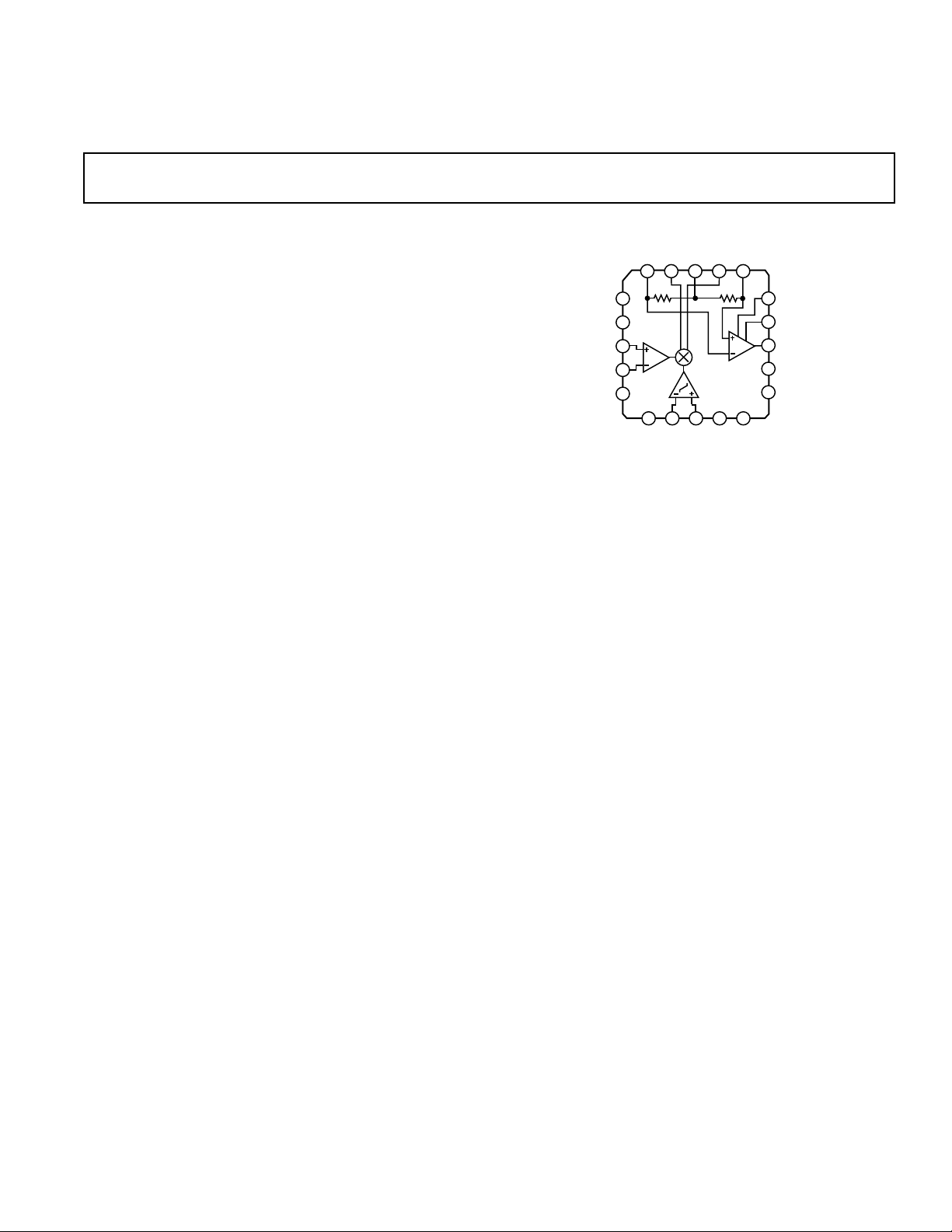
FUNCTIONAL BLOCK DIAGRAM
Doubly-Balanced Mixer
Low Distortion
+24 dBm Third Order Intercept (IP3)
+10 dBm 1 dB Compression Point
Low LO Drive Required: –10 dBm
Bandwidth
500 MHz RF and LO Input Bandwidths
250 MHz Differential Current IF Output
DC to >200 MHz Single-Ended Voltage IF Output
Single or Dual Supply Operation
DC Coupled Using Dual Supplies
All Ports May Be DC Coupled
No Lower Frequency Limit—Operation to DC
User-Programmable Power Consumption
APPLICATIONS
High Performance RF/IF Mixer
Direct to Baseband Conversion
Image-Reject Mixers
I/Q Modulators and Demodulators
filtering. When building a quadrature-amplitude modulator or
image reject mixer, the differential current outputs of two
AD831s may be summed by connecting them together.
An integral low noise amplifier provides a single-ended voltage
PRODUCT DESCRIPTION
The AD831 is a low distortion, wide dynamic range, monolithic
mixer for use in such applications as RF to IF down conversion
in HF and VHF receivers, the second mixer in DMR base stations, direct-to-baseband conversion, quadrature modulation and demodulation, and doppler-shift detection in ultrasound imaging applications. The mixer includes an LO driver
and a low-noise output amplifier and provides both user-programmable power consumption and 3rd-order intercept point.
The AD831 provides a +24 dBm third-order intercept point for
–10 dBm LO power, thus improving system performance and
reducing system cost compared to passive mixers, by eliminating
the need for a high power LO driver and its attendant shielding
and isolation problems.
The RF, IF, and LO ports may be dc or ac coupled when the
mixer is operating from ±5 V supplies or ac coupled when operating from a single supply of 9 V minimum. The mixer operates
output and can drive such low impedance loads as filters, 50 Ω
amplifier inputs, and A/D converters. Its small signal bandwidth
exceeds 200 MHz. A single resistor connected between pins
OUT and FB sets its gain. The amplifier’s low dc offset allows
its use in such direct-coupled applications as direct-to-baseband
conversion and quadrature-amplitude demodulation.
The mixer’s SSB noise figure is 10.3 dB at 70 MHz using its
output amplifier and optimum source impedance. Unlike passive mixers, the AD831 has no insertion loss and does not require an external diplexer or passive termination.
A programmable-bias feature allows the user to reduce power
consumption, with a reduction in the 1 dB compression point
and third-order intercept. This permits a tradeoff between dynamic range and power consumption. For example, the AD831
may be used as a second mixer in cellular and two-way radio
base stations at reduced power while still providing a substantial
performance improvement over passive solutions.
with RF and LO inputs as high as 500 MHz.
The mixer’s IF output is available as either a differential current
output or a single-ended voltage output. The differential output
is from a pair of open collectors and may be ac coupled via a
transformer or capacitor to provide a 250 MHz output bandwidth. In down-conversion applications, a single capacitor connected across these outputs implements a low-pass filter to
reduce harmonics directly at the mixer core, simplifying output
REV. B
Information furnished by Analog Devices is believed to be accurate and
reliable. However, no responsibility is assumed by Analog Devices for its
use, nor for any infringements of patents or other rights of third parties
which may result from its use. No license is granted by implication or
otherwise under any patent or patent rights of Analog Devices.
PRODUCT HIGHLIGHTS
1. –10 dBm LO Drive for a +24 dBm Output Referred Third
Order Intercept Point
2. Single-Ended Voltage Output
3. High Port-to-Port Isolation
4. No Insertion Loss
5. Single or Dual Supply Operation
6. 10.3 dB Noise Figure
© Analog Devices, Inc., 1995
One Technology Way, P.O. Box 9106, Norwood. MA 02062-9106, U.S.A.
Tel: 617/329-4700 Fax: 617/326-8703
Page 2

(TA = +258C and 6VS = 65 V unless otherwise noted;
AD831–SPECIFICA TIONS
all values in dBm assume 50 V load.)
Parameter Conditions Min Typ Max Units
RF INPUT
Bandwidth –10 dBm Signal Level, IP3 ≥ +20 dBm 400 MHz
10.7 MHz IF and High Side Injection
See Figure 1
1 dB Compression Point 10 dBm
Common-Mode Range ±1V
Bias Current DC Coupled 160 500 µA
DC Input Resistance Differential or Common Mode 1.3 kΩ
Capacitance 2pF
IF OUTPUT
Bandwidth Single-Ended Voltage Output, –3 dB
Level = 0 dBm,
RL = 100 Ω 200 MHz
Conversion Gain Terminals OUT and VFB Connected 0 dB
Output Offset Voltage DC Measurement; LO Input Switched ± 1 –40 15 +40 mV
Slew Rate 300 V/µs
Output Voltage Swing R
= 100 Ω, Unity Gain ±1.4 V
L
Short Circuit Current 75 mA
LO INPUT
Bandwidth –10 dBm Input Signal Level 400 MHz
10.7 MHz IF and High Side Injection
Maximum Input Level –1 +1 V
Common-Mode Range –1 +1 V
Minimum Switching Level Differential Input Signal 200 mV p-p
Bias Current DC Coupled 17 50 µA
Resistance Differential or Common Mode 500 Ω
Capacitance 2pF
ISOLATION BETWEEN PORTS
LO to RF LO = 100 MHz, R
LO to IF LO = 100 MHz, R
= 50 Ω, 10.7 MHz IF 70 dB
S
= 50 Ω, 10.7 MHz IF 30 dB
S
RF to IF RF = 100 MHz, RS = 50 Ω, 10.7 MHz IF 45 dB
DISTORTION AND NOISE LO = –10 dBm, f = 100 MHz, IF = 10.7 MHz
3rd Order Intercept Output Referred, ± 100 mV LO Input 24 dBm
2rd Order Intercept Output Referred, ± 100 mV LO Input 62 dBm
1 dB Compression Point R
= 100 Ω, R
L
= ∞ 10 dBm
BIAS
Noise Figure, SSB Matched Input, RF = 70 MHz, IF = 10.7 MHz 10.3 dB
Matched Input, RF = 150 MHz, IF = 10.7 MHz 14 dB
POWER SUPPLIES
Recommended Supply Range Dual Supply ±4.5 ±5.5 V
Single Supply 9 11 V
For Best 3rd Order Intercept Point Performance 100 125 mA
Quiescent Current
1
BIAS Pin Open Circuited
NOTES
1
Quiescent current is programmable.
Specifications subject to change without notice.
–2–
REV. B
Page 3
AD831
GND
VN
VN
RFP
RFN
AN
IFN
AP
VP
IFP
VP
LON
GND
LOP
VP
COM
VFB
BIAS
OUT
VN
1931220
4
5
8
6
7
12 1391110
18
17
14
16
15
TOP VIEW
(Not to Scale)
AD831
ABSOLUTE MAXIMUM RATINGS
1
Supply Voltage ±VS . . . . . . . . . . . . . . . . . . . . . . . . . . ±5.5 V
Input Voltages
RFHI, RFLO . . . . . . . . . . . . . . . . . . . . . . . . . . . . . . . . ±3 V
LOHI, LOLO . . . . . . . . . . . . . . . . . . . . . . . . . . . . . . . ±1 V
Internal Power Dissipation
2
. . . . . . . . . . . . . . . . . . 1200 mW
Operating Temperature Range
AD831A . . . . . . . . . . . . . . . . . . . . . . . . . . . –40°C to +85°C
Storage Temperature Range . . . . . . . . . . . . –65°C to +150°C
Lead Temperature Range (Soldering 60 sec) . . . . . . . . +300°C
NOTES
1
Stresses above those listed under “Absolute Maximum Ratings” may cause
permanent damage to the device. This is a stress rating only and functional
operation of the device at these or any other conditions above those indicated in the
operational section of this specification is not implied. Exposure to absolute
maximum rating conditions for extended periods may affect device reliability.
2
Thermal Characteristics:
20-Pin PLCC Package: θJA = 110°C/Watt; θJC = 20°C/Watt.
Note that the θJA = 110°C/W value is for the package measured while suspended
in still air; mounted on a PC board, the typical value is θ
conduction provided by the AD831’s package being in contact with the board,
which serves as a heat sink.
= 90°C/W due to the
JA
ORDERING GUIDE
Temperature Package Package
Model Range Description Option
AD831AP –40°C to +85°C 20-Lead PLCC P-20A
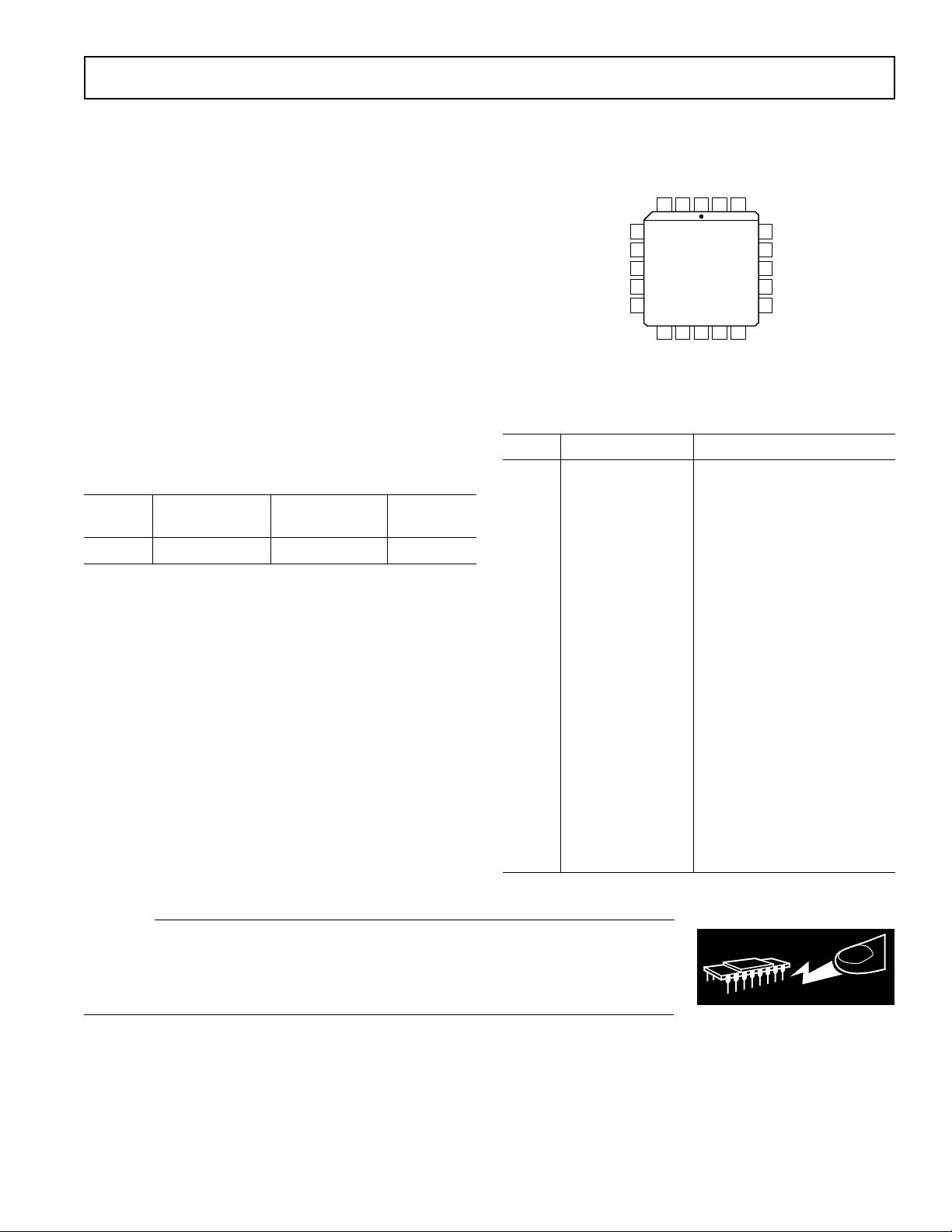
PIN CONFIGURATION
20-Lead PLCC
PIN DESCRIPTION
Pin Mnemonic Description
1 VP Positive Supply Input
2 IFN Mixer Current Output
3 AN Amplifier Negative Input
4 GND Ground
5 VN Negative Supply Input
6 RFP RF Input
7 RFN RF Input
8 VN Negative Supply Input
9 VP Positive Supply Input
10 LON Local Oscillator Input
11 LOP Local Oscillator Input
12 VP Positive Supply Input
13 GND Ground
14 BIAS Bias Input
15 VN Negative Supply Input
16 OUT Amplifier Output
17 VFB Amplifier Feedback Input
18 COM Amplifier Output Common
19 AP Amplifier Positive Input
20 IFP Mixer Current Output
CAUTION
ESD (electrostatic discharge) sensitive device. Electrostatic charges as high as 4000 V readily
accumulate on the human body and test equipment and can discharge without detection.
Although the AD831 features proprietary ESD protection circuitry, permanent damage may
occur on devices subjected to high energy electrostatic discharges. Therefore, proper ESD
precautions are recommended to avoid performance degradation or loss of functionality.
–3–
REV. B
WARNING!
ESD SENSITIVE DEVICE
Page 4
AD831–Typical Characteristics
FREQUENCY – MHz
80
70
0
40
30
20
10
50
60
10 1000100
ISOLATION – dB
3 x RF-to-IF
2 x RF-to-IF
RF-to-IF
3 x RF-to-IF
2 x RF-to-IF
RF-to-IF
30
25
20
15
10
THIRD ORDER INTERCEPT – dBm
5
0
10 1000100
FREQUENCY – MHz
Figure 1. Third-Order Intercept vs. Frequency,
IF Held Constant at 10.7 MHz
80
70
60
50
40
30
ISOLATION – dB
20
10
0
10 1000100
FREQUENCY – MHz
65
64
63
62
61
SECOND ORDER INTERCEPT – dBm
60
10 1000100
FREQUENCY – MHz
Figure 4. Second-Order Intercept vs. Frequency
90
80
70
60
50
40
ISOLATION – dB
30
20
10
0
10 1000100
FREQUENCY – MHz
Figure 2. IF-to-RF Isolation vs. Frequency
60
2 x LO-to-IF
50
3 x LO-to-IF
40
30
ISOLATION – dB
20
10
0
10 1000100
Figure 3. LO-to-IF Isolation vs. Frequency
LO
FREQUENCY – MHz
–4–
Figure 5. LO-to-RF Isolation vs. Frequency
Figure 6. RF-to-IF Isolation vs. Frequency
REV. B
Page 5
AD831
FREQUENCY – MHz
1dB COMPRESSION POINT – dBm
11
10
7
0 600100 200 300 400 500
9
8
LO LEVEL = –10dBm
IF = 10.7MHz
V
S
= 8V
V
S
= 9V
12
10
8
6
4
1dB COMPRESSION POINT – dBm
2
0
10 1000100
FREQUENCY – MHz
Figure 7. 1 dB Compression Point vs. Frequency, Gain = 1
12
10
8
6
4
1dB COMPRESSION POINT – dBm
2
0
10 1000100
FREQUENCY – MHz
1.00
0.75
0.50
0.25
0.00
–0.25
GAIN ERROR – dB
–0.50
–0.75
–1.00
10 1000100
FREQUENCY – MHz
Figure 10. Gain Error vs. Frequency, Gain = 1
9
8
7
6
5
4
3
2
1dB COMPRESSION POINT – dBm
1
0
10 1000100
FREQUENCY – MHz
Figure 8. 1 dB Compression Point vs. RF Input, Gain = 2
25
MIXER OUTPUT
TRANSFORMER
22
COUPLED PER FIGURE 18
19
16
13
REV. B
THIRD ORDER INTERCEPT – dBm
10
100 350250150 200 300
Figure 9. Third-Order Intercept vs. Frequency , LO Held
Constant at 241 MHz
FREQUENCY – MHz
MIXER PLUS AMPLIFIER,
G = 1
Figure 11. 1 dB Compression Pointvs.Frequency,Gain = 4
Figure 12. Input 1 dB Compression Point vs. Frequency,
Gain = 1, 9 V Single Supply
–5–
Page 6

AD831–Typical Characteristics
FREQUENCY – MHz
1200
1000
0
50 250100 150 200
800
600
400
200
INPUT RESISTANCE – Ohms
4.0
3.5
3.0
2.5
2.0
INPUT CAPACITANCE – pF
INPUT RESISTANCE
INPUT CAPACITANCE
30
25
VS = 8V
20
LO LEVEL = –10dBm
IF = 10.7MHz
THIRD ORDER INTERCEPT – dBm
∆f = 20kHz
15
0 50050 100 150 200 250 300 350 400 450
FREQUENCY – MHz
VS = 9V
Figure 13. Input Third Order Intercept, 9 V Single Supply
62.4
62.2
62.0
61.8
61.6
61.4
61.2
61.0
60.8
60.6
SECOND ORDER INTERCEPT – dBm
60.4
60.2
LO LEVEL = –10dBm
IF = 10.7MHz
∆f = 20kHz
0 50050 100 150 200 250 300 350 400 450
VS = 9V
VS = 8V
FREQUENCY – MHz
Figure 14. Input Second Order Intercept,
9 V Single Supply
Figure 15. Input Impedance vs. Frequency, ZIN = RiC
18
17
16
15
14
13
12
11
NOISE FIGURE – dB
10
9
8
50 250100 150 200
FREQUENCY – MHz
Figure 16. Noise Figure vs. Frequency,
Matched Input
–6–
REV. B
Page 7

AD831
THEORY OF OPERATION
The AD831 consists of a mixer core, a limiting amplifier, a low
noise output amplifier, and a bias circuit (Figure 17).
The mixer’s RF input is converted into differential currents by a
highly linear, Class A voltage-to-current converter, formed by
transistors Q1, Q2 and resistors R1, R2. The resulting currents
drive the differential pairs Q3, Q4 and Q5, Q6. The LO input is
through a high gain, low noise limiting amplifier that converts
the –10 dBm LO input into a square wave. This square wave
drives the differential pairs Q3, Q4 and Q5, Q6 and produces a
high level output at IFP and IFN—consisting of the sum and
difference frequencies of the RF and LO inputs—and a series of
lower level outputs caused by odd harmonics of the LO frequency mixing with the RF input.
An on-chip network supplies the bias current to the RF and LO
inputs when these are ac coupled; this network is disabled when
the AD831 is dc coupled.
19 3
ANAP
20 2
IFP
18mA TYP
IFN
18mA TYP
When the integral output amplifier is used, pins IFN and IFP
are connected directly to pins AFN and AFP; the on-chip load
resistors convert the output current into a voltage that drives the
output amplifier. The ratio of these load resistors to resistors
R1, R2 provides nominal unity gain (0 dB) from RF to IF. The
expression for the gain, in decibels, is
GdB= 20 log
4
10
π
1
π
Equation 1
2
2
where
4
is the amplitude of the fundamental component of a square wave
π
1
is the conversion loss
2
π
is the small signal dc gain of the AD831 when the LO input
2
is driven fully positive or negative.
VP
1
50Ω
50Ω
20Ω
20Ω
BIAS
LOCAL
OSCILLATOR
INPUT
RF
INPUT
LOP
LON
RFP
RFN
BIAS
A
O
11
10
6
7
VP
VN
LIMITING
AMPLIFIER
Q2
BIAS
CURRENT
Q3
R4
1kΩ
R1
20ΩR220Ω
Q7
36mA TYP 27mA TYP
1kΩ
R3
26Ω
Q6Q4
Q5
R5
Q1
5kΩ
5kΩ
CURRENT
MIRROR
12mA TYP
50Ω
BIAS
50Ω
36Ω
16
OUT
17
VFB
18
COM
Figure 17. Simplified Schematic Diagram
REV. B
–7–
Page 8

AD831
The mixer has two open-collector outputs (differential currents) at pins IFN and IFP. These currents may be used to provide nominal unity RF-to-IF gain by connecting a center-tapped
transformer (1:1 turns ratio) to pins IFN and IFP as shown in
Figure 18.
IF OUTPUT
LOCAL
OSCILLATOR
INPUT
RF
INPUT
LOP
LON
RFP
RFN
BIAS
VP
VN
11
10
6
7
LIMITING
AMPLIFIER
Q2
BIAS
CURRENT
Q3
MCLT4-1H
VPOS
18mA TYP
R4
1kΩ
R1
20ΩR220Ω
36mA TYP
20 2
IFP
Q6Q4
Q5
R5
1kΩ
Q1
Q7
R3
26Ω
VP
1
IFN
18mA TYP
5kΩ
5kΩ
Figure 18. Connections for Transformer Coupling to the IF
Output
Programming the Bias Current
Because the AD831’s RF port is a Class-A circuit, the maximum RF input is proportional to the bias current. This bias current may be reduced by connecting a resistor from the BIAS pin
to the positive supply (Figure 19). For normal operation, the
BIAS pin is left unconnected. For lowest power consumption,
the BIAS pin is connected directly to the positive supply. The
range of adjustment is 100 mA for normal operation to
45 mA total current at minimum power consumption.
2
3 19
IFN VP IFP AP
AN
4
5
6
7
8
50Ω
GND
VN
RFP
RFN
VN
LON
VP
9 10 11 12 13
1
AD831
Top View
LOP
20
50Ω
COM
18
VFB
17
OUT
16
VPOS
15
VN
1.33kΩ
14
BIAS
GND
VP
0.1µF
NOTE ADDED
RESISTOR
Low-Pass Filtering
A simple low-pass filter may be added between the mixer and
the output amplifier by shunting the internal resistive loads (an
equivalent resistance of about 14 Ω with a tolerance of 20%)
with external capacitors; these attenuate the sum component in
a down-conversion application (Figure 20). The corner frequency of this one-pole low-pass filter (f = (2 π RC
)–1) should
F
be placed about an octave above the difference frequency IF.
Thus, for a 70 MHz IF, a –3 dB frequency of 140 MHz might
be chosen, using C
= (2 × π × 14 Ω × 140 MHz)–1 ≈ 82 pF, the
F
nearest standard value.
CF = =
C
2
3 19
IFN VP IFP AP
AN
4
5
6
7
8
50Ω
GND
VN
RFP
RFN
VN
LON
VP
9 10 11 12 13
2 π f R
F
1
LOP
89.7 f
C
F
20
50Ω
AD831
Top View
VP
GND
COM
VFB
OUT
VN
BIAS
18
17
16
15
14
1
1
Figure 20. Low-Pass Filtering Using External Capacitors
Using the Output Amplifier
The AD831’s output amplifier converts the mixer core’s differential current output into a single-ended voltage and provides
an output as high as ±1 V peak into a 50 Ω load (+10 dBm).
For unity gain operation (Figure 21), the inputs AN and AP
connect to the open-collector outputs of the mixer’s core and
OUT connects to VFB.
2
3 19
IFN VP IFP AP
AN
4
5
6
7
8
50Ω
GND
VN
RFP
RFN
VN
LON
VP
9 10 11 12 13
1
AD831
Top View
LOP
20
50Ω
COM
18
VFB
17
OUT
16
15
VN
14
BIAS
GND
VP
IF
OUTPUT
Figure 19. Programming the Quiescent Current
Figure 21. Output Amplifier Connected for Unity Gain
Operation
–8–
REV. B
Page 9

AD831
FREQUENCY – MHz
12
10
0
10 1000100
1dB COMPRESSION POINT – dBm
8
6
4
2
G = 1
G = 2
G = 4
For gains other than unity, the amplifier’s output at OUT is
connected via an attenuator network to VFB; this determines
the overall gain. Using resistors R1 and R2 (Figure 22), the gain
setting expression is
GdB= 20 log
2
3 19
IFN VP IFP AP
AN
4
5
6
7
8
50Ω
GND
VN
RFP
RFN
VN
LON
VP
9 10 11 12 13
10
20
1
AD831
Top View
LOP
VP
R1+ R2
50Ω
GND
Equation 2
R2
COM
18
VFB
OUT
VN
BIAS
R2
17
R1
16
15
14
IF
OUTPUT
Figure 22. Output Amplifier Feedback Connections for
Increasing Gain
Driving Filters
The output amplifier can be used for driving reverse-terminated
loads. When driving an IF bandpass filter (BPF), for example,
proper attention must be paid to providing the optimal source
and load terminations so as to achieve the specified filter response. The AD831’s wideband highly linear output amplifier
affords an opportunity to increase the RF-to-IF gain to compensate for a filter’s insertion and termination losses.
Figure 23 indicates how the output amplifier’s low impedance
(voltage source) output can drive a doubly-terminated bandpass
filter. The typical 10 dB of loss (4 dB of insertion loss and 6 dB
due to the reverse-termination) be made up by the inclusion of a
feedback network that increases the gain of the amplifier by
10 dB (×3.162). When constructing a feedback circuit, the signal path between OUT and VFB should be as short as possible.
2
3 19
IFN VP IFP AP
AN
4
5
6
7
8
50Ω
GND
VN
RFP
RFN
VN
LON
VP
9 10 11 12 13
1
AD831
Top View
LOP
20
50Ω
COM
18
R2
51.1Ω
VFB
17
R1
110Ω
OUT
16
15
VN
14
BIAS
GND
VP
BPF
R
T
R
T
IF
OUTPUT
Figure 23. Connections for Driving a Doubly-Terminated
Bandpass Filter
Higher gains can be achieved, using different resistor ratios, but
with concomitant reduction in the bandwidth of this amplifier
(Figure 24). Note also that the Johnson noise of these gain-setting resistors, as well as that of the BPF terminating resistors, is
ultimately reflected back to the mixer’s input; thus they should
be as small as possible, consistent with the permissible loading
on the amplifier’s output.
REV. B
Figure 24. Output Amplifier 1 dB Compression Point for
Gains of 1, 2, and 4 (Gains of 0 dB, 6 dB, and 12 dB,
Respectively)
–9–
Page 10

AD831
APPLICATIONS
Careful component selection, circuit layout, power supply
decoupling, and shielding are needed to minimize the AD831’s
susceptibility to interference from radio and TV stations, etc. In
bench evaluation, we recommend placing all of the components
in a shielded box and using feedthrough decoupling networks
for the supply voltage.
Circuit layout and construction are also critical, since stray capacitances and lead inductances can form resonant circuits and
are a potential source of circuit peaking, oscillation, or both.
Dual-Supply Operation
Figure 25 shows the connections for dual supply operation.
Supplies may be as low as ±4.5 V but should be no higher than
±5.5 V due to power dissipation.
+5V
C
F
82pF
2
1
IFN VP IFP AP
LON
LOP
51.1Ω
INPUT
3 19
AN
4
0.1µF
5
C2
RF
C1
L1
0.1µF
–5V
–5V
6
7
8
+5V
50Ω
GND
VN
RFP
RFN
VN
VP
9 10 11 12 13
0.1µF
The RF input to the AD831 is shown connected by an impedance matching network for an assumed source impedance of
50 Ω. Figure 15 shows the input impedance of the AD831 plotted vs. frequency. The input circuit can be modeled as a resistance in parallel with a capacitance. The 82 pF capacitors (C
)
F
connected from IFN and IFP to VP provide a low-pass filter
with a cutoff frequency of approximately 140 MHz in downconversion applications (see the Theory of Operation section of
this data sheet for more details). The LO input is connected
single-ended because the limiting amplifier provides a symmetric drive to the mixer. To minimize intermodulation distortion,
connect pins OUT and VFB by the shortest possible path. The
connections shown are for unity-gain operation.
At LO frequencies less than 100 MHz, the AD831’s LO power
may be as low as –20 dBm for satisfactory operation. Above
100 MHz, the specified LO power of –10 dBm must be used.
0.1µF
C
F
82pF
20
50Ω
COM
18
51.1Ω
VFB
17
AD831
Top View
VP
0.1µF
+5V
GND
OUT
VN
BIAS
110Ω
16
15
14
NC
R
0.1µF
T
BPF
–5V
R
T
IF
OUTPUT
LO INPUT
–10 dBm
Figure 25. Connections for ±5 V Dual-Supply Operation Showing Impedance
Matching Network and Gain of 2 for Driving Reverse-Terminated IF Filter
–10–
REV. B
Page 11

AD831
Single Supply Operation
Figure 26 is similar to the dual supply circuit in Figure 19. Supplies may be as low as 9 V but should not be higher than
11 V due to power dissipation. As in Figure 19, both the RF
and LO ports are driven single-ended and terminated.
+9V
0.1µF
82pF
82pF
INPUT
2
3 19
IFN VP IFP AP
AN
4
5
C2
C1
RF
L1
0.1µF
6
7
8
+9V
50Ω
GND
VN
RFP
RFN
VN
LON
VP
9 10 11 12 13
0.1µF
51.1Ω
1
AD831
Top View
LOP
0.1µF0.1µF
+9V
20
VP
0.1µF
In single supply operation, the COM terminal is the “ground”
reference for the output amplifier and must be biased to 1/2 the
supply voltage, which is done by resistors R1 and R2. The OUT
pin must be ac-coupled to the load.
+5V
R2
51.1Ω
0.1µF
R1
110Ω
R
C
C
T
IF
OUTPUT
50Ω
GND
COM
VFB
OUT
VN
BIAS
5kΩ
18
5kΩ
17
16
15
14
NC
LO INPUT
–10 dBm
Figure 26. Connections for +9 V Single-Supply Operation
REV. B
–11–
Page 12

AD831
Connections Quadrature Demodulation
Two AD831 mixers may have their RF inputs connected in parallel and have their LO inputs driven in phase quadrature (Figure 27) to provide demodulated in-phase (I) and quadrature
C
F
2
3 19
IFN VP IFP AP
AN
50Ω
GND
VN
RFP
RFN
VN
LON
VP
9 10 11 12 13
51.1Ω
0.1µF
LO INPUT
AT 90°
–10 dBm
C
F
INPUT
4
0.1µF
0.1µF
IF
51.1Ω
–5V
–5V
5
6
7
8
+5V
(Q) outputs. The mixers’ inputs may be connected in parallel
and a single termination resistor used if the mixers are located in
close proximity on the PC board.
+5V
0.1µF
C
F
20
1
50Ω
COM
18
VFB
17
AD831
Top View
LOP
+5V
0.1µF
C
OUT
16
15
VN
14
BIAS
GND
VP
0.1µF
+5V
F
0.1µF
NC
–5V
DEMODULATED
QUADRATURE
OUTPUT
0.1µF
0.1µF
–5V
–5V
2
3 19
AN
4
5
6
7
8
+5V
50Ω
GND
VN
RFP
RFN
VN
LON
VP
9 10 11 12 13
0.1µF
LO INPUT
AT 0°
–10 dBm
IFN VP IFP AP
51.1Ω
1
AD831
Top View
LOP
+5V
20
VP
50Ω
0.1µF
GND
COM
VFB
OUT
VN
BIAS
18
17
16
15
14
0.1µF
NC
Figure 27. Connections for Quadrature Demodulation
–5V
DEMODULATED
IN-PHASE
OUTPUT
–12–
REV. B
Page 13

AD831
Table I. AD831 Mixer Table, 64.5 V Supplies, LO = –9 dBm
LO Level –9.0 dBm, LO Frequency 130.7 MHz, Data File imdTB10771
RF Level 0.0 dBm, RF Frequency 120 MHz
Temperature Ambient
Dut Supply ±4.50 V
VPOS Current 90 mA
VNEG Current 91 mA
Intermodulation Table RF harmonics (rows) × LO harmonics (columns).
First row absolute value of nRF-mLO, and second row is the sum.
01234567
0 –32.7 –35.7 –21.1 –11.6 –19.2 –35.1 –41.9
–32.7 –35.7 –21.1 –11.6 –19.2 –35.1 –41.9
1 –31.6 0.0 –37.2 –41.5 –30.4 –34.3 –25.2 –40.1
–31.6 –28.5 –26.7 –28.0 –27.2 –33.2 –34.3 –44.8
2 –45.3 –48.2 –39.4 –57.6 –44.9 –42.4 –40.2 –40.2
–45.3 –42.4 –49.4 –42.5 –51.1 –46.2 –58.1 –61.6
3 –54.5 –57.1 –57.5 –50.6 –62.6 –55.8 –59.7 –55.2
–54.5 –65.5 –46.0 –63.7 –60.6 –69.6 –72.7 –73.5
4 –67.1 –63.1 –69.9 –69.9 –69.6 –74.1 –69.7 –58.6
–67.1 –53.6 –72.9 –71.2 –70.1 –72.6 –73.5 –72.7
5 –53.5 –62.6 –73.8 –72.3 –70.7 –71.1 –74.3 –73.0
–53.5 –68.4 –70.8 –72.8 –73.4 –73.2 –73.3 –72.5
6 –73.6 –57.7 –68.6 –73.1 –73.8 –73.0 –72.9 –74.4
–73.6 –73.5 –72.7 –73.5 –73.6 –73.1 –72.4 –73.7
7 –73.8 –73.9 –63.4 –72.6 –74.6 –74.9 –73.6 –74.5
–73.8 –73.8 –73.2 –73.8 –72.6 –73.7 –73.5 –72.9
Table II. AD831 Mixer Table, 65 V Supplies, LO = –9 dBm
LO Level –9.0 dBm, LO Frequency 130.7 MHz, Data File imdTB13882
RF Level 0.0 dBm, RF Frequency 120 MHz
Temperature Ambient
Dut Supply ±5.00 V
VPOS Current 102 mA
VNEG Current 102 mA
Intermodulation table RF harmonics (rows) × LO harmonics (columns).
First row absolute value of nRF-mLO, and second row is the sum.
01234567
0 –36.5 –46.5 –33.0 –17.0 –23.0 –34.2 –45.6
–36.5 –46.5 –33.0 –17.0 –23.0 –34.2 –45.6
1 –37.5 0.0 –41.2 –41.1 –38.5 –29.0 –31.7 –47.4
–37.5 –29.1 –38.7 –22.9 –28.4 –35.3 –34.3 –52.4
2 –45.9 –45.2 –47.6 –61.5 –53.7 –43.5 –41.5 –41.8
–45.9 –39.4 –35.7 –38.4 –42.3 –53.7 –52.8 –66.3
3 –46.4 –53.0 –67.0 –43.0 –60.9 –47.9 –50.7 –41.0
–46.4 –40.0 –50.0 –48.9 –57.8 –57.0 –71.8 –67.4
4 –45.1 –56.0 –48.7 –64.6 –53.5 –55.7 –53.5 –51.1
–45.1 –39.0 –48.1 –58.4 –56.1 –63.8 –70.5 –67.6
5 –35.2 –45.3 –54.1 –54.1 –53.7 –57.9 –66.6 –64.3
–35.2 –53.0 –62.4 –67.3 –67.0 –69.4 –73.2 –72.9
6 –63.4 –41.1 –53.6 –66.5 –58.8 –63.3 –61.7 –71.4
–63.4 –66.3 –67.2 –67.5 –72.9 –71.2 –71.7 –73.2
7 –67.3 –65.8 –37.8 –54.6 –62.5 –71.7 –55.2 –57.1
–67.3 –61.6 –66.3 –72.9 –71.4 –70.7 –72.1 –73.1
REV. B
–13–
Page 14

AD831
Table III. AD831 Mixer Table, 63.5 V Supplies, LO = –20 dBm
LO Level –20.0 dBm, LO Frequency 130.7 MHz, Data File G1T1K 0771
RF Level 0.0 dBm, RF Frequency 120 MHz
Temperature Ambient
Dut Supply ±3.50 V
VPOS Current 55 mA
VNEG Current 57 mA
Intermodulation Table RF harmonics (rows) × LO harmonics (columns).
First row absolute value of nRF-mLO, and second row is the sum.
01234567
0 –45.2 –35.7 –16.1 –21.6 –22.3 –32.0 –36.4
–45.2 –35.7 –16.1 –21.6 –22.3 –32.0 –36.4
1 –30.3 0.0 –33.7 –47.9 –37.5 –33.8 –32.0 –45.2
–30.3 –29.7 –28.2 –24.4 –26.0 –47.4 –35.9 –49.7
2 –50.3 –49.4 –47.4 –49.9 –48.8 –38.5 –40.7 –51.0
–50.3 –41.0 –51.4 –34.7 –49.8 –48.6 –68.5 –67.9
3 –48.4 –55.7 –58.2 –45.0 –57.0 –68.4 –55.5 –47.7
–48.4 –52.9 –50.0 –64.5 –62.8 –73.4 –74.0 –71.8
4 –66.7 –59.7 –67.2 –62.8 –58.2 –71.5 –72.9 –63.5
–66.7 –65.9 –78.1 –74.2 –77.5 –74.4 –77.9 –77.5
5 –66.9 –71.5 –73.6 –77.6 –70.8 –70.2 –75.8 –78.1
–66.9 –76.3 –78.1 –78.2 –78.1 –78.0 –77.9 –77.9
6 –78.0 –69.7 –76.7 –78.6 –78.8 –75.4 –78.1 –79.0
–78.0 –78.3 –78.3 –78.2 –78.1 –78.0 –77.9 –77.8
7 –78.4 –78.5 –76.9 –78.7 –79.0 –79.1 –78.6 –78.9
–78.4 –78.3 –78.2 –78.2 –77.9 –77.9 –77.8 –77.5
Table IV. AD831 Mixer Table, 65 V Supplies, 1 kV Bias Resistor, LO = –20 dBm
LO Level –20.0 dBm, LO Frequency 130.7 MHz, Data File G1T1K 3881
RF Level 0.0 dBm, RF Frequency 120 MHz
Temperature Ambient
Dut Supply ±3.50 V
VPOS Current 59 mA
VNEG Current 61 mA
Intermodulation table RF harmonics (rows) × LO harmonics (columns).
First row absolute value of nRF-mLO, and second row is the sum.
01234567
0 –60.6 –52.3 –16.6 –12.8 –26.0 –45.0 –38.8
–60.6 –52.3 –16.6 –12.8 –26.0 –45.0 –38.8
1 –34.1 0.0 –35.2 –41.8 –29.8 –29.1 –35.3 –49.0
–34.1 –27.3 –28.7 –20.7 –32.9 –39.2 –38.2 –47.8
2 –46.6 –48.8 –40.1 –52.2 –57.9 –38.6 –45.8 –47.7
–46.6 –37.8 –47.6 –41.7 –54.2 –50.4 –64.1 –64.9
3 –41.3 –58.8 –59.5 –41.8 –61.2 –58.1 –57.5 –54.0
–41.3 –47.9 –65.2 –62.5 –64.2 –73.8 –72.3 –72.6
4 –53.9 –52.5 –73.7 –68.1 –60.3 –71.0 –63.4 –62.3
–53.9 –61.4 –70.6 –76.9 –76.8 –78.6 –78.3 –78.1
5 –66.9 –65.8 –76.6 –75.2 –65.4 –70.0 –73.6 –68.7
–66.9 –69.7 –72.9 –77.4 –77.7 –78.5 –78.4 –78.2
6 –77.4 –73.3 –73.8 –78.8 –79.2 –73.6 –74.9 –79.3
–77.4 –78.6 –78.7 –78.6 –78.6 –78.4 –78.2 –78.2
7 –78.9 –79.0 –77.9 –78.0 –79.3 –79.5 –79.3 –79.3
–78.9 –78.8 –78.7 –78.6 –78.3 –78.3 –78.1 –78.0
–14–
REV. B
Page 15

AD831
HP 8656B
SYNTHESIZED
SIGNAL GENERATOR
HP 8656A
SYNTHESIZED
SIGNAL GENERATOR
HP 8656B
SYNTHESIZED
SIGNAL GENERATOR
HP 6632A
PROGRAMMABLE
POWER SUPPLY
–5V
50Ω
MCL
ZFSC-2-1
COMBINER
IEEE CONTROLLER
DISK DRIVE
∑
HP 9920
HP 9121
HP 6632A
PROGRAMMABLE
POWER SUPPLY
+5V
SIGNAL GENERATOR
AD831
PER
FIGURE 25
LO
FLUKE 6082A
SYNTHESIZED
Figure 28. Third-Order Intercept Characterization Setup
HP 6632A
PROGRAMMABLE
POWER SUPPLY
–5V
50Ω
50Ω
MCL
ZFSC-2-1
HP 6632A
PROGRAMMABLE
POWER SUPPLY
+5V
RF IF
AD831
PER
FIGURE 25
LO
HP 8561E
SPECTRUM
ANALYZER
IEEE-488 BUS
HP 8656B
SYNTHESIZED
SIGNAL GENERATOR
50Ω
HP 8561E
SPECTRUM
ANALYZER
50Ω
SYNTHESIZED
SIGNAL GENERATOR
HP 8656B
MCL
ZFSC-2-1
USED FOR
IF TO RF, LO
LO TO RF
MOVE SPECTRUM
ANALYZER FOR IF
MEASUREMENTS
Figure 29. IF to RF Isolation Characterization Setup
REV. B
–15–
Page 16

AD831
OUTLINE DIMENSIONS
Dimensions shown in inches and (mm).
20-Lead PLCC (P-20A)
0.048 (1.21)
0.042 (1.07)
0.050
(1.27)
BSC
0.020
(0.50)
0.048 (1.21)
0.042 (1.07)
4
8
R
PIN 1
IDENTIFIER
TOP VIEW
9
0.356 (9.04)
0.350 (8.89)
0.395 (10.02)
0.385 (9.78)
0.056 (1.42)
0.042 (1.07)
19 3
18
14
13
SQ
SQ
0.180 (4.57)
0.165 (4.19)
C1879a–10–6/95
0.110 (2.79)
0.085 (2.16)
0.025 (0.63)
0.015 (0.38)
0.021 (0.53)
0.013 (0.33)
0.032 (0.81)
0.026 (0.66)
0.040 (1.01)
0.025 (0.64)
0.330 (8.38)
0.290 (7.37)
C1879a–10–7/95
–16–
PRINTED IN U.S.A.
REV. B
 Loading...