

Page 1
0.1 GHz–2.5 GHz, 70 dB
a
FEATURES
Wide Bandwidth: 0.1 GHz to 2.5 GHz Min
High Dynamic Range: 70 dB to ⴞ3.0 dB
High Accuracy: ⴞ1.0 dB over 65 dB Range (@ 1.9 GHz)
Fast Response: 40 ns Full-Scale Typical
Controller Mode with Error Output
Scaling Stable Over Supply and Temperature
Wide Supply Range: +2.7 V to +5.5 V
Low Power: 40 mW at 3 V
Power-Down Feature: 60 W at 3 V
Complete and Easy to Use
APPLICATIONS
RF Transmitter Power Amplifier Setpoint
Control and Level Monitoring
Logarithmic Amplifier for RSSI Measurement
Cellular Base Stations, Radio Link, Radar
PRODUCT DESCRIPTION
The AD8313 is a complete multistage demodulating logarithmic amplifier, capable of accurately converting an RF signal at
its differential input to an equivalent decibel-scaled value at its
dc output. The AD8313 maintains a high degree of log conformance for signal frequencies from 0.1 GHz to 2.5 GHz and
is useful over the range of 10 MHz to 3.5 GHz. The nominal
input dynamic range is –65 dBm to 0 dBm (re: 50 Ω), and the
sensitivity can be increased by 6 dB or more with a narrow band
input impedance matching network or balun. Application is
straightforward, requiring only a single supply of 2.7 V–5.5 V
and the addition of a suitable input and supply decoupling.
Operating on a 3 V supply, its 13.7 mA consumption (for T
+25°C) amounts to only 41 mW. A power-down feature is
provided; the input is taken high to initiate a low current
(20 µA) sleep mode, with a threshold at half the supply voltage.
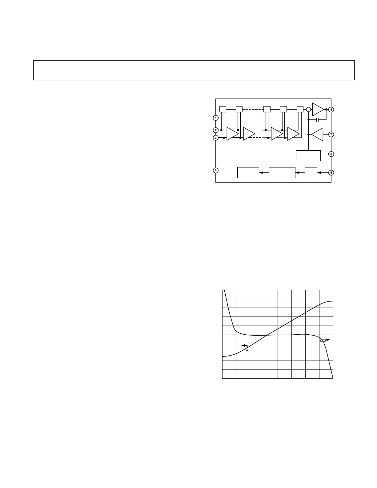
The AD8313 uses a cascade of eight amplifier/limiter cells,
each having a nominal gain of 8 dB and a –3 dB bandwidth of
3.5 GHz, for a total midband gain of 64 dB. At each amplifier
output, a detector (rectifier) cell is used to convert the RF signal
to baseband form; a ninth detector cell is placed directly at the
input of the AD8313. The current-mode outputs of these cells
are summed to generate a piecewise linear approximation to the
logarithmic function, and converted to a low impedance voltagemode output by a transresistance stage, which also acts as a lowpass filter.
=
A
Logarithmic Detector/Controller
AD8313
FUNCTIONAL BLOCK DIAGRAM
NINE DETECTOR CELLS
++ ++
VPOS
INHI
INLO
VPOS
8dB8dB
EIGHT 8dB 3.5GHz AMPLIFIER STAGES
AD8313
SLOPE
CONTROL
8dB 8dB
BAND-GAP
REFERENCE
When used as a log amp, the scaling is determined by a separate
feedback interface (a transconductance stage) that sets the slope
to approximately 18 mV/dB; used as a controller, this stage
accepts the setpoint input. The logarithmic intercept is positioned to nearly –100 dBm, and the output runs from about
0.45 V dc at –73 dBm input to 1.75 V dc at 0 dBm input. The
scale and intercept are supply and temperature stable.
The AD8313 is fabricated on Analog Devices’ advanced
25 GHz silicon bipolar IC process and is available in a 8-lead
µSOIC package. The operating temperature range is –40°C to
+85°C. An evaluation board is available.
2.0
FREQUENCY = 1.9GHz
1.8
1.6
1.4
1.2
1.0
0.8
0.6
OUTPUT VOLTAGE – Volts DC
0.4
0.2
0
–70 –60 –50 –40 –30 –20 –10
–80
INPUT AMPLITUDE – dBm
Figure 1. Typical Logarithmic Response and Error vs.
Input Amplitude
+
IvV
LP
INTERCEPT
CONTROL
GAIN
BIAS
C
INT
VvI
VOUT
VSET
COMM
PWDN
5
4
3
2
1
0
–1
–2
OUTPUT ERROR – dB
–3
–4
–5
0
REV. B
Information furnished by Analog Devices is believed to be accurate and
reliable. However, no responsibility is assumed by Analog Devices for its
use, nor for any infringements of patents or other rights of third parties
which may result from its use. No license is granted by implication or
otherwise under any patent or patent rights of Analog Devices.
One Technology Way, P.O. Box 9106, Norwood, MA 02062-9106, U.S.A.
Tel: 781/329-4700 World Wide Web Site: http://www.analog.com
Fax: 781/326-8703 © Analog Devices, Inc., 1999
Page 2

AD8313–SPECIFICATIONS
(@ TA = +25ⴗC, VS = +5.0 V1, R
Parameter Conditions Min
≥ 10 k⍀ unless otherwise noted)
L
2
Typ Max
2
SIGNAL INPUT INTERFACE
Specified Frequency Range 0.1 2.5 GHz
DC Common-Mode Voltage V
Input Bias Currents 10 µA
Input Impedance fRF < 100 MHz
LOG (RSSI) MODE Sinusoidal, input termination configuration shown in Figure 27.
100 MHz
5
±3 dB Dynamic Range
6
Nominal Conditions
3
53.5 65 dB
– 0.75 V
POS
900储1.1 Ω储pF
Range Center –31.5 dBm
±1 dB Dynamic Range 56 dB
Slope 17 19 21 mV/dB
Intercept –96 –88 –80 dBm
+2.7 V ≤ V
≤ +5.5 V, –40°C ≤ T ≤ +85°C
S
±3 dB Dynamic Range 51 64 dB
Range Center –31 dBm
±1 dB Dynamic Range 55 dB
Slope 16 19 22 mV/dB
Intercept –99 –89 –75 dBm
Temperature Sensitivity P
900 MHz
5
= –10 dBm –0.022 dB/°C
IN
Nominal Conditions
±3 dB Dynamic Range 60 69 dB
Range Center –32.5 dBm
±1 dB Dynamic Range 62 dB
Slope 15.5 18 20.5 mV/dB
Intercept –105 –93 –81 dBm
+2.7 V ≤ V
≤ +5.5 V, –40°C ≤ T ≤ +85°C
S
±3 dB Dynamic Range 55.5 68.5 dB
Range Center –32.75 dBm
±1 dB Dynamic Range 61 dB
Slope 15 18 21 mV/dB
Intercept –110 –95 –80 dBm
Temperature Sensitivity P
1.9 GHz
7
= –10 dBm –0.019 dB/°C
IN
Nominal Conditions
±3 dB Dynamic Range 52 73 dB
Range Center –36.5 dBm
±1 dB Dynamic Range 62 dB
Slope 15 17.5 20.5 mV/dB
Intercept –115 –100 –85 dBm
+2.7 V ≤ V
≤ +5.5 V, –40°C ≤ T ≤ +85°C
S
±3 dB Dynamic Range 50 73 dB
Range Center 36.5 dBm
±1 dB Dynamic Range 60 dB
Slope 14 17.5 21.5 mV/dB
Intercept –125 –101 –78 dBm
Temperature Sensitivity P
2.5 GHz
7
= –10 dBm –0.019 dB/°C
IN
Nominal Conditions
±3 dB Dynamic Range 48 66 dB
Range Center –34 dBm
±1 dB Dynamic Range 46 dB
Slope 16 20 25 mV/dB
Intercept –111 –92 –72 dBm
+2.7 V ≤ V
≤ +5.5 V, –40°C ≤ T ≤ +85°C
S
±3 dB Dynamic Range 47 68 dB
Range Center –34.5 dBm
±1 dB Dynamic Range 46 dB
Slope 14.5 20 25 mV/dB
Intercept –128 –92 –56 dBm
Temperature Sensitivity P
= –10 dBm –0.040 dB/°C
IN
Units
4
–2–
REV. B
Page 3

AD8313
Parameter Conditions Min
3.5 GHz
5
2
Typ Max
±3 dB Dynamic Range 43 dB
±1 dB Dynamic Range 35 dB
Slope 24 mV/dB
Intercept –65 dBm
CONTROL MODE
Controller Sensitivity f = 900 MHz 23 V/dB
Low Frequency Gain VSET to VOUT
Open-Loop Corner Frequency VSET to VOUT
8
8
84 dB
700 Hz
Open-Loop Slew Rate f = 900 MHz 2.5 V/µs
VSET Delay Time 150 ns
VOUT INTERFACE
Current Drive Capability
Source Current 400 µA
Sink Current 10 mA
Minimum Output Voltage Open Loop 50 mV
Maximum Output Voltage Open Loop V
Output Noise Spectral Density P
Small Signal Response Time P
= –60 dBm, f
IN
= –60 dBm, f
P
IN
= –60 dBm to –57 dBm, 10% to 90% 40 60 ns
IN
= 100 Hz 2.0 µV/√Hz
SPOT
= 10 MHz 1.3 µV/√Hz
SPOT
– 0.1 V
POS
Large Signal Response Time PIN = No Signal to 0 dBm, Settled to 0.5 dB 110 160 ns
VSET INTERFACE
Input Voltage Range 0 V
Input Impedance 18k储1 Ω储pF
POWER-DOWN INTERFACE
PWDN Threshold V
/2 V
POS
Power-Up Response Time Time delay following HI to LO transition
until device meets full specifications. 1.8 µs
PWDN Input Bias Current PWDN = 0 V 5 µA
PWDN = V
S
<1 µA
POWER SUPPLY
Operating Range +2.7 +5.5 V
Powered Up Current 13.7 15.5 mA
+4.5 V ≤ V
+2.7 V ≤ V
Powered Down Current +4.5 V ≤ V
≤ +5.5 V, –40°C ≤ T ≤ +85°C 18.5 mA
S
≤ +3.3 V, –40°C ≤ T ≤ +85°C 18.5 mA
S
≤ +5.5 V, –40°C ≤ T ≤ +85°C 50 150 µA
S
+2.7 V ≤ VS ≤ +3.3 V, –40°C ≤ T ≤ +85°C2050µA
NOTES
1
Except where otherwise noted, performance at VS = +3.0 V is equivalent to +5.0 V operation.
2
Minimum and maximum specified limits on parameters that are guaranteed but not tested are six sigma values.
3
Input impedance shown over frequency range in Figure 24.
4
Double slashes (储) denote “in parallel with.”
5
Linear regression calculation for error curve taken from –40 dBm to –10 dBm for all parameters.
6
Dynamic range refers to range over which the linearity error remains within the stated bound.
7
Linear regression calculation for error curve taken from –60 dBm to –5 dBm for 3 dB dynamic range. All other regressions taken from –40 dBm to –10 dBm.
8
AC response shown in Figure 10.
Specifications subject to change without notice.
2
POS
Units
V
–3–REV. B
Page 4
AD8313
WARNING!
ESD SENSITIVE DEVICE
ABSOLUTE MAXIMUM RATINGS*
Supply Voltage VS . . . . . . . . . . . . . . . . . . . . . . . . . . . . . . 5.5 V
VOUT, VSET, PWDN . . . . . . . . . . . . . . . . . . . . . . 0 V, VPOS
Input Power Differential (re: 50 Ω, 5.5 V) . . . . . . . . . +25 dBm
Input Power Single-Ended (re: 50 Ω, 5.5 V) . . . . . . . +19 dBm
Internal Power Dissipation . . . . . . . . . . . . . . . . . . . . .200 mW
. . . . . . . . . . . . . . . . . . . . . . . . . . . . . . . . . . . . . . . 200°C/W
θ
JA
Maximum Junction Temperature . . . . . . . . . . . . . . . . +125°C
Operating Temperature Range . . . . . . . . . . . . –40°C to +85°C
Storage Temperature Range . . . . . . . . . . . . . –65°C to +150°C
Lead Temperature Range (Soldering 60 sec) . . . . . . . . +300°C
*Stresses above those listed under Absolute Maximum Ratings may cause perma-
nent damage to the device. This is a stress rating only; functional operation of the
device at these or any other conditions above those indicated in the operational
section of this specification is not implied. Exposure to absolute maximum rating
conditions for extended periods may effect device reliability.
PIN CONFIGURATION
VPOS
INHI
INLO
VPOS
1
2
AD8313
TOP VIEW
3
(Not to Scale)
4
8
7
6
5
VOUT
VSET
COMM
PWDN
ORDERING GUIDE
PIN FUNCTION DESCRIPTIONS
Pin Name Description
1, 4 VPOS Positive supply voltage (VPOS), +2.7 V to
+5.5 V.
2 INHI Noninverting Input. This input should be
ac coupled.
3 INLO Inverting Input. This input should be ac
coupled.
5 PWDN Connect pin to ground for normal operat-
ing mode. Connect pin to supply for power-
down mode.
6 COMM Device Common.
7 VSET Setpoint input for operation in controller
mode. To operate in RSSI mode, short
VSET and VOUT.
8 VOUT Logarithmic/Error Output.
Temperature Package Package Brand
Model Range Descriptions Option Code
AD8313ARM –40°C to +85°C 8-Lead µSOIC RM-08 J1A
AD8313ARM-REEL –40°C to +85°C 13” Tape and Reel RM-08 J1A
AD8313ARM-REEL7 –40°C to +85°C 7” Tape and Reel RM-08 J1A
AD8313-EVAL Evaluation Board
CAUTION
ESD (electrostatic discharge) sensitive device. Electrostatic charges as high as 4000 V readily
accumulate on the human body and test equipment and can discharge without detection. Although
the AD8313 features proprietary ESD protection circuitry, permanent damage may occur on
devices subjected to high energy [>250 V HBM] electrostatic discharges. Therefore, proper ESD
precautions are recommended to avoid performance degradation or loss of functionality.
–4–
REV. B
Page 5

Typical Performance Characteristics–
AD8313
2.0
VS = +5V
1.8
INPUT MATCH SHOWN IN FIGURE 27
1.6
1.4
1.2
1.0
– Volts
OUT
0.8
V
0.6
0.4
0.2
0
–70
6
4
2
0
ERROR – dB
–2
1.9GHz
–4
–6
–70 10–60
1.9GHz
900MHz
–60 –50 –40 –30 –20 –10 0 10
Figure 2. V
900MHz
INPUT AMPLITUDE – dBm
OUT
100MHz
2.5GHz
–50 –40 –30 –20 –10
INPUT AMPLITUDE – dBm
2.5GHz
vs. Input Amplitude
VS = +5V
INPUT MATCH SHOWN IN FIGURE 27
2.5GHz
100MHz
100MHz
1.9GHz
Figure 3. Log Conformance vs. Input Amplitude
900MHz
0
2.0
VS = +5V
1.8
INPUT MATCH SHOWN IN FIGURE 27
1.6
1.4
1.2
1.0
– Volts
OUT
0.8
V
0.6
0.4
SLOPE AND INTERCEPT NORMALIZED AT +258C
0.2
AND APPLIED TO –408C AND +858C
0
–60 –50 –40 –30 –20 –10 0 10
–70
Figure 5. V
OUT
at 900 MHz; –40
2.0
VS = +5V
1.8
INPUT MATCH SHOWN IN FIGURE 27
1.6
–408C
1.4
1.2
+258C
1.0
– Volts
OUT
0.8
+858C
V
0.6
0.4
SLOPE AND INTERCEPT NORMALIZED AT +258C
0.2
AND APPLIED TO –408C AND +858C
0
–60 –50 –40 –30 –20 –10 0 10
–70
Figure 6. V
OUT
at 1.9 GHz; –40
5
4
3
2
–408C
+258C
+858C
INPUT AMPLITUDE – dBm
1
0
–1
–2
–3
–4
–5
ERROR – dB
and Log Conformance vs. Input Amplitude
°
C, +25°C and +85°C
5
4
3
2
1
0
–1
ERROR – dB
–2
–3
–4
–5
INPUT AMPLITUDE – dBm
and Log Conformance vs. Input Amplitude
°
C, +25°C and +85°C
2.0
VS = +5V
1.8
INPUT MATCH SHOWN IN FIGURE 27
1.6
1.4
1.2
1.0
– Volts
OUT
0.8
V
0.6
0.4
SLOPE AND INTERCEPT NORMALIZED AT +258C
0.2
AND APPLIED TO –408C AND +858C
0
–60 –50 –40 –30 –20 –10 0 10
–70
Figure 4. V
OUT
at 100 MHz; –40
5
4
3
2
–408C
+258C
+858C
INPUT AMPLITUDE – dBm
1
0
–1
–2
–3
–4
–5
ERROR – dB
and Log Conformance vs. Input Amplitude
°
C, +25°C and +85°C
– Volts
OUT
V
Figure 7. V
at 2.5 GHz; –40
–5–REV. B
2.0
1.8
1.6
1.4
1.2
1.0
0.8
0.6
0.4
0.2
VS = +5V
INPUT MATCH SHOWN IN FIGURE 27
–408C
+258C
SLOPE AND INTERCEPT
NORMALIZED AT +258C AND
APPLIED TO –408C AND +858C
+858C
0
–70
–60 –50 –40 –30 –20 –10 0 10
and Log Conformance vs. Input Amplitude
OUT
INPUT AMPLITUDE – dBm
°
C, +25°C and +85°C
5
4
3
2
1
0
–1
–2
–3
–4
–5
ERROR – dB
Page 6

AD8313
22
21
20
19
SLOPE – mV/dB
18
17
16
0 2500500
Figure 8. V
+85
°
C
24
23
22
21
20
19
18
SLOPE – mV/dB
17
16
15
14
2.5
VPS = +5V
INPUT MATCH SHOWN IN FIGURE 27
+858C
+258C
–408C
1000 1500 2000
FREQUENCY – MHz
Slope vs. Frequency; –40°C, +25°C and
OUT
SPECIFIED OPERATING RANGE
2.5GHz
100MHz
900MHz
1.9GHz
3.0 3.5 4.0 4.5 5.0 5.5 6.0
SUPPLY VOLTAGE – V
–70
–80
–90
INTERCEPT – dBm
–100
–110
0 2500500
Figure 11. V
+85
°
C
–70
–75
–80
–85
–90
–95
INTERCEPT – dBm
–100
–105
–110
2.5
VPS = +5V
INPUT MATCH SHOWN IN FIGURE 27
+858C
+258C
–408C
1000 1500 2000
FREQUENCY – MHz
Intercept vs. Frequency; –40°C, +25°C and
OUT
SPECIFIED OPERATING RANGE
100MHz
2.5GHz
900MHz
1.9GHz
3.0 3.5 4.0 4.5 5.0 5.5 6.0
SUPPLY VOLTAGE – V
Figure 9. V
REF LEVEL = 92dB
GAIN – dB
OUT
TO V
SET
V
100 1k 10k 100k 1M
Figure 10. AC Response from V
Slope vs. Supply Voltage
OUT
SCALE: 10dB/DIV
FREQUENCY – Hz
SET
to V
OUT
Figure 12. V
10
2GHz RF INPUT
V
= +5.5V
S
INPUT MATCH SHOWN
IN FIGURE 27
1
mV/ Hz
0.1
100
Figure 13. V
Intercept vs. Supply Voltage
OUT
RF INPUT
–70dBm
–60dBm
–55dBm
–50dBm
–45dBm
–40dBm
–35dBm
–30dBm
1k 10k 100k 1M 10M
FREQUENCY – Hz
Noise Spectral Density
OUT
–6–
REV. B
Page 7

100.00
CH. 1
CH. 1 GND
CH. 2 GND
CH. 2
CH. 1 & CH. 2: 200mV/DIV AVERAGE: 50 SAMPLES
VS = +5.5V
VS = +2.7V
HORIZONTAL: 50ns/DIV
PULSED RF
100MHz, –45dBm
CH. 1 & CH. 2: 500mV/DIV
AVERAGE: 50 SAMPLES
HORIZONTAL: 50ns/DIV
CH. 1 GND
CH. 2 GND
PULSED RF
100MHz, 0dBm
CH. 1
CH. 2
VS = +5.5V
V
S
= +2.7V
AD8313
10.00
1.00
SUPPLY CURRENT – mA
0.10
0.01
0
13.7mA
V
= +3V
POS
12 34 5
PWDN VOLTAGE – V
POS
= +5VV
20mA
40mA
Figure 14. Typical Supply Current vs. PWDN Voltage
CH. 1 & CH. 2: 1V/DIV CH. 3: 5V/DIV
V
@
OUT
= +5.5V
V
CH. 1 GND
CH. 2 GND
CH. 3 GND
HORIZONTAL: 1ms/DIV
S
V
V
S
PWDN
@
OUT
= +2.7V
Figure 17. Response Time, No Signal to –45 dBm
Figure 15. PWDN Response Time
HP8648B
SIGNAL
GENERATOR
10MHz REF OUTPUT
RF OUT
10V
+V
S
0.01mF
0.01mF
10V
+V
S
PIN = 0dBm
0.1mF
54.9V
0.1mF
1
VPOS VOUT
AD8313
2
INHI
3
INLO
4
VPOS
Figure 16. Test Setup for PWDN Response Time
8
7
VSET
6
COMM
5
PWDN
EXT TRIG
TEK P6205
FET PROBE
0603 SIZE SURFACE
MOUNT COMPONENTS ON
A LOW LEAKAGE PC BOARD
HP8112A
PULSE
GENERATOR
TEK
TDS784C
SCOPE
OUT
TRIG
Figure 18. Response Time, No Signal to +0 dBm
HP8648B
SIGNAL
GENERATOR
PULSE
MODULATION
MODE
RF OUT
RF
SPLITTER
–6dB
+V
S
0.01mF
+V
S
10MHz REF OUTPUT
PULSE MODE IN OUT
–6dB
10V
0.01mF
10V
0.1mF
54.9V
0.1mF
1
2
3
4
VPOS
AD8313
INHI
INLO
VPOS
VOUT
VSET
COMM
PWDN
EXT TRIG
8
7
6
5
FET PROBE
HP8112A
PULSE
GENERATOR
TEK P6205
0603 SIZE SURFACE
MOUNT COMPONENTS ON
A LOW LEAKAGE PC BOARD
TEK
TDS784C
SCOPE
TRIG
OUT
Figure 19. Test Setup for RSSI-Mode Pulse Response
TRIG
–7–REV. B
Page 8

AD8313
CIRCUIT DESCRIPTION
The AD8313 is essentially an 8-stage logarithmic amplifier,
specifically designed for use in RF measurement and power
amplifier control applications at frequencies up to 2.5 GHz. A
block diagram is shown in Figure 20. (For a full treatment of
log-amp theory and design principles, consult the AD8307
data sheet).
NINE DETECTOR CELLS
VPOS
INHI
INLO
VPOS
++ ++
8dB8dB
EIGHT 8dB 3.5GHz AMPLIFIER STAGES
AD8313
SLOPE
CONTROL
8dB 8dB
BAND-GAP
REFERENCE
+
IvV
LP
INTERCEPT
CONTROL
GAIN
BIAS
C
INT
VvI
VOUT
VSET
COMM
PWDN
Figure 20. Block Diagram
A fully-differential design is used, and the inputs INHI and INLO
(Pins 2 and 3) are internally biased to approximately 0.75 V
below the supply voltage, and present a low frequency imped-
ance of nominally 900 Ω in parallel with 1.1 pF. The noise
spectral density referred to the input is 0.6 nV/√Hz, equivalent
to a voltage of 35 µV rms in a 3.5 GHz bandwidth, or a noise
power of –76 dBm re: 50 Ω. This sets the lower limit to the
dynamic range; the Applications section shows how to increase
the sensitivity by the use of a matching network or input transformer. However, the low end accuracy of the AD8313 is enhanced
by specially shaping the demodulation transfer characteristic to
partially compensate for errors due to internal noise.
Each of the eight cascaded stages has a nominal voltage gain of
8 dB and a bandwidth of 3.5 GHz, and is supported by precision biasing cells which determine this gain and stabilize it
against supply and temperature variations. Since these stages are
direct-coupled and the dc gain is high, an offset-compensation
loop is included. The first four of these stages, and the biasing
system, are powered from Pin 4, while the later stages and the
output interfaces are powered from Pin 1. The biasing is controlled by a logic interface PWDN (Pin 5); this is grounded for
normal operation, but may be taken high (to V
chip. The threshold is at V
/2 and the biasing functions are
POS
) to disable the
S
enabled and disabled within 1.8 µs.
Each amplifier stage has a detector cell associated with its output. These nonlinear cells essentially perform an absolute-value
(full-wave rectification) function on the differential voltages
along this backbone, in a transconductance fashion; their outputs are in current-mode form and are thus easily summed. A
ninth detector cell is added at the input of the AD8313. Since
the mid-range response of each of these nine detector stages is
separated by 8 dB, the overall dynamic range is about 72 dB
(Figure 21). The upper end of this range is determined by the
capacity of the first detector cell, and occurs at approximately
0 dBm. The practical dynamic range is over 70 dB, to the
±3 dB error points. However, some erosion of this range will
occur at temperature and frequency extremes. Useful operation to
over 3 GHz is possible, and the AD8313 remains serviceable at
10 MHz (see Typical Performance Characteristics), needing
only a small amount of additional ripple filtering.
2.0
1.8
1.6
1.4
1.2
1.0
– Volts
OUT
0.8
V
0.6
0.4
0.2
0
–90
SLOPE = 18mV/dB
INTERCEPT = –100dBm
–70 –60 –50 –40 –30 –20 –10
–80
INPUT AMPLITUDE – dBm
5
4
3
2
1
0
–1
–2
–3
–4
–5
0
ERROR – dB
Figure 21. Typical RSSI Response and Error vs. Input
Power at 1.9 GHz
The fluctuating current output generated by the detector cells,
with a fundamental component at twice the signal frequency, is
filtered first by a low-pass section inside each cell, and also by
the output stage. The output stage converts these currents to a
voltage, V
, at pin VOUT (Pin 8), which can swing “rail-to-
OUT
rail.” The filter exhibits a two-pole response with a corner at
approximately 12 MHz and full-scale rise time (10%–90%) of
40 ns. The residual output ripple at an input frequency of
100 MHz has an amplitude of under 1 mV. The output can
drive a small resistive load: it can source currents of up to
400 µA, and sink up to 10 mA. The output is stable with any
capacitive load, though settling time may be impaired. The low
frequency incremental output impedance is approximately 0.2 Ω.
In addition to its use as an RF power measurement device (that
is, as a logarithmic amplifier) the AD8313 may also be used in
controller applications, by breaking the feedback path from
VOUT to the VSET (Pin 7), which determines the slope of the
output (nominally 18 mV/dB). This pin becomes the setpoint
input in controller modes. In this mode, the voltage V
OUT
remains close to ground (typically under 50 mV) until the decibel
equivalent of the voltage V
V
makes a rapid transition to a voltage close to V
OUT
is reached at the input, when
SET
POS
(see
controller mode). The logarithmic intercept is nominally posi-
tioned at –100 dBm (re: 50 Ω) and this is effective in both the
log amp mode and the controller mode.
Thus, with Pins 7 and 8 connected (log amp mode) we have:
V
where P
= V
OUT
is the input power, stated in dBm when the source is
IN
(PIN + 100 dBm)
SLOPE
directly terminated in 50 Ω. However, the input impedance of
the AD8313 is much higher than 50 Ω and the sensitivity of this
device may be increased by about 12 dB by using some type of
matching network (see below), which adds a voltage gain and
lowers the intercept by the same amount. This dependence on
the choice of reference impedance can be avoided by restating
the expression as:
where V
= 20 × V
V
OUT
is the rms value of a sinusoidal input appearing
IN
× log (VIN/2.2 µV)
SLOPE
across Pins 2 and 3; here, 2.2 µV corresponds to the intercept,
expressed in voltage terms. (For a more thorough treatment of
the effect of signal waveform and metrics on the intercept positioning for a log amp, see the AD8307 data sheet).
–8–
REV. B
Page 9

AD8313
COMM
g
m
STAGE
C
INT
LP
LM
10mA
MAX
VOUT
C
L
BIAS
I
SOURCE
400mA
VPOS
FROM
SET-POINT
SUMMED
DETECTOR
OUTPUTS
6
8
1
With Pins 7 and 8 disconnected (controller mode), the output
may be stated as
V
v VS when V
OUT
V
v 0 when V
OUT
(PIN + 100) > V
SLOPE
(PIN + 100) < V
SLOPE
SET
SET
when the input is stated in terms of the power of a sinusoidal
signal across a net termination impedance of 50 Ω. The transi-
tion zone between high and low states is very narrow, since the
output stage behaves essentially as a fast integrator. The above
equations may be restated as
V
v VS when V
OUT
V
v 0 when V
OUT
SLOPE
SLOPE
log (V
log (V
/2.2 µV) > V
IN
/2.2 µV) < V
IN
SET
SET
A further use of the separate VOUT and VSET pins is in raising
the load-driving current capability by the inclusion of an external NPN emitter follower. More complete information about
usage in these various modes is provided in the Applications
section.
INTERFACES
This section describes the signal and control interfaces and their
behavior. On-chip resistances and capacitances exhibit varia-
tions of up to ±20%. These resistances are sometimes tempera-
ture dependent and the capacitances may be voltage dependent.
Power-Down Interface, PWDN
The power-down threshold is accurately centered at the midpoint
of the supply as shown in Figure 22. If Pin 5 is left unconnected or
tied to the supply voltage (recommended) the bias enable current is shut off, and the current drawn from the supply is pre-
dominately through a nominal 300 kΩ chain (20 µA at 3 V). When
grounded, the bias system is turned on. The threshold level is
accurately at V
/2. The input bias current at the PWDN pin
POS
when operating in the device “ON” state is approximately
5 µA for V
POS
VPOS
PWDN
COMM
= 3 V.
4
5
6
75kV
50kV
150kV
150kV
TO BIAS
ENABLE
1.24V
TO STAGES
1 THRU 4
TO 2ND
STAGE
COMM
VPOS
INHI
INLO
VPOS
1
0.5pF
2
3
0.5pF
4
~
0.75V
2.5kV 2.5kV
1.25kV
(1ST DETECTOR)
0.7pF
250V
125V
125V
~
1.4mA
1.25kV
GAIN BIAS
Figure 23. Input Interface Simplified Schematic
For high frequency use, Figure 24 shows the input impedance
plotted on a Smith chart. This measured result of a typical de-
vice includes a 191 mil 50 Ω trace and a 680 pF capacitor to
ground from the INLO pin.
Frequency
R
100MHz
900MHz
1.9GHz
2.5GHz
650
55
22
23
+j X
–j 400
–j 135
–j 65
–j 43
AD8313 MEASURED
2.5GHz
1.9GHz
100MHz
900MHz
1.1pF900V
Figure 24. Typical Input Impedance
Logarithmic/Error Output, VOUT
The rail-to-rail output interface is shown in Figure 25. V
OUT
can run from within about 50 mV of ground, to within about
100 mV of the supply voltage, and is short-circuit safe to either
supply. However, the sourcing load current I
SOURCE
is limited by
that provided by the PNP transistor, to typically 400 µA. Larger
load currents can be provided by adding an external NPN transistor (see Applications). The dc open-loop gain of this amplifier
is high, and it may be regarded essentially as an integrator having a capacitance of 2 pF (C
) driven by the current-mode
INT
signals generated by the summed outputs of the nine detector
stages, which is scaled approximately 4.0 µA/dB.
Figure 22. Power-Down Threshold Circuitry
Signal Inputs, INHI, INLO
The simplest low frequency ac model for this interface consists
of just a 900 Ω resistance R
pacitance, C
connected across INHI and INLO. Figure 23
IN
in shunt with a 1.1 pF input ca-
IN
shows these distributed in the context of a more complete schematic. The input bias voltage shown is for the enabled chip;
when disabled, it will rise by a few hundred millivolts. If the
input is coupled via capacitors, this change may cause a lowlevel signal transient to be introduced, having a time-constant
formed by these capacitors and R
valued coupling capacitors should be well matched; this is not
necessary when using the small capacitors found in many impedance transforming networks used at high frequencies.
. For this reason, large-
IN
Figure 25. Output Interface Circuitry
Thus, for a midscale RF input of about 3 mV, which is some
40 dB above the minimum detector output, this current is
160 µA and the output changes by 8 V/µs. When VOUT is
connected to VSET, the rise and fall times are approximately
40 ns (for R
≥ 10 kΩ). The nominal slew rate is ±2.5 V/µs.
L
The HF compensation technique results in stable operation with
a large capacitive load, C
will then be limited by I
, though the positive-going slew rate
L
SOURCE/CL
to 1 V/µs for C
= 400 pF.
L
–9–REV. B
Page 10

AD8313
Setpoint Interface, VSET
The setpoint interface is shown in Figure 26. The voltage V
SET
is divided by a factor of three in a resistive attenuator of total
resistance 18 kΩ. The signal is converted to a current by the
action of the op amp and the resistor R3 (1.5 kΩ), which bal-
ances the current generated by the summed output of the nine
detector cells at the input to the previous cell. The logarithmic
slope is nominally 3 × 4.0 µA/dB × 1.5 kΩ ≈ 18 mV/dB.
1
VPOS
VSET
COMM
R1
12kV
8
R2
6kV
6
FDBK
25mA25mA
TO O/P
STAGE
LP
R3
1.5kV
Figure 26. Setpoint Interface Circuitry
APPLICATIONS
Basic Connections for Log (RSSI) Mode
Figure 27 shows the AD8313 connected in its basic measurement mode. A power supply of +2.7 V to +5.5 V is required.
The power supply to each of the VPOS pins should be decoupled
with a 0.1 µF, surface mount ceramic capacitor and a series
resistor of 10 Ω.
The PWDN pin is shown as grounded. The AD8313 may be
disabled by a logic “HI” at this pin. When disabled, the chip
current is reduced to about 20 µA from its normal value of
13.7 mA. The logic threshold is at V
/2 and the enable func-
POS
tion occurs in about 1.8 µs; note, however, that further settling
time is generally needed at low input levels. While the input in
this case is terminated with a simple 50 Ω broadband resistive
match, there are a wide variety of ways in which the input termination can be accomplished. These are discussed in the Input
Coupling section.
VSET is connected to VOUT to establish a feedback path that
controls the overall scaling of the logarithmic amplifier. The
load resistance, R
, should not be lower than 5 kΩ in order that
L
the full-scale output of 1.75 V can be generated with the limited
available current of 400 µA max.
As stated in the Absolute Maximum Ratings, an externally applied overvoltage on the VOUT pin that is outside the range 0 V
to V
is sufficient to cause permanent damage to the device. If
POS
overvoltages are expected on the VOUT pin, a series resistor
) should be included as shown. A 500 Ω resistor is suffi-
(R
PROT
cient to protect against overvoltage up to ±5 V; 1000 Ω should
be used if an overvoltage of up to ±15 V is expected. Since the
output stage is meant to drive loads of no more than 400 µA,
this resistor will not impact device performance for more high
impedance drive applications (higher output current applications
are discussed in the Increasing Output Current section).
R1
10V
+V
S
680pF
680pF
R2
10V
+V
S
0.1mF
53.6V
0.1mF
1
VPOS VOUT
AD8313
2
INHI
3
INLO
4
VPOS
VSET
COMM
PWDN
R
PROT
8
7
6
5
RL = 1MV
Figure 27. Basic Connections for Log (RSSI) Mode
Operating in the Controller Mode
Figure 28 shows the basic connections for operation in controller mode. The link between VOUT and VSET is broken and a
“setpoint” is applied to VSET. Any difference between V
and the equivalent input power to the AD8313, will drive V
either to the supply rail or close to ground. If V
than the equivalent input power, V
will be driven towards
OUT
SET
SET
OUT
is greater
ground and vice versa.
R1
10V
+V
S
R3
10V
+V
S
0.1mF
0.1mF
1
VPOS VOUT
AD8313
2
INHI
3
INLO
4
VPOS
VSET
COMM
PWDN
R
PROT
8
7
6
5
CONTROLLER
OUTPUT
V
SETPOINT
INPUT
Figure 28. Basic Connections for Operation in the
Controller Mode
This mode of operation is useful in applications where the output power of an RF power amplifier (PA) is to be controlled by
an analog AGC loop (Figure 29). In this mode, a setpoint
voltage, proportional in dB to the desired output power, is applied to the VSET pin. A sample of the output power from the
PA, via a directional coupler or other means, is fed to the input
of the AD8313.
ENVELOPE OF
TRANSMITTED
SIGNAL
POWER
DIRECTIONAL
COUPLER
AMPLIFIER
AD8313
RFIN
VOUT
VSET
RF IN
SETPOINT
CONTROL DAC
Figure 29. Setpoint Controller Operation
V
is applied to the gain control terminal of the power ampli-
OUT
fier. The gain control transfer function of the power amplifier
should be an inverse relationship, i.e., increasing voltage decreases gain.
–10–
REV. B
Page 11
AD8313
L
MATCH
C1
C2
C
IN
R
IN
AD8313
50V
50V SOURCE
A positive input step on V
creased power from the PA) will drive V
(indicating a demand for in-
SET
towards ground.
OUT
This should be arranged to increase the gain of the PA. The
loop will settle when V
power to the AD8313 to the dB equivalent of V
settles to a voltage that sets the input
OUT
SET
.
Input Coupling
The signal may be coupled to the AD8313 in a variety of ways.
In all cases, there must not be a dc path from the input pins to
ground. Some of the possibilities include: dual input coupling
capacitors, a flux-linked transformer, a printed-circuit balun,
direct drive from a directional coupler, or a narrow-band impedance matching network.
Figure 30 shows a simple broadband resistive match. A termina-
tion resistor of 53.6 Ω combines with the internal input imped-
ance of the AD8313 to give an overall resistive input impedance
of approximately 50 Ω. The termination resistor should prefer-
ably be placed directly across the input pins, INHI to INLO,
where it serves to lower the possible deleterious effects of dc
offset voltages on the low end of the dynamic range. At low
frequencies, this may not be quite as attractive, since it necessitates the use of larger coupling capacitors. The two 680 pF
input coupling capacitors set the high-pass corner frequency of
the network at 9.4 MHz.
50V SOURCE
50V
C1
680pF
C2
680pF
R
MATCH
53.6V
AD8313
C
IN
R
IN
3
2
1
MATCHED
0
ERROR – dB
–1
–2
–3
–80 –70 –60 –50 –40 –30 –20 –10
–90 100
BALANCED
TERMINATED
DR = 66dB
BALANCED
DR = 71dB
MATCHED
DR = 69dB
INPUT AMPLITUDE – dBm
Figure 31. Comparison of Terminated, Matched and
Balanced Input Drive at 900 MHz
3
TERMINATED
2
1
0
BALANCED
ERROR – dB
–1
–2
DR = 75dB
MATCHED
MATCHED
DR = 73dB
BALANCED
DR = 75dB
TERMINATED
Figure 30. A Simple Broadband Resistive Input Termination
The high pass corner frequency can be set higher according to
the equation:
1
=
C
250
×××π
where:
C
CC
×
12
=
CC
+
12
f
dB3
In high frequency applications, the use of a transformer, balun
or matching network is advantageous. The impedance matching characteristics of these networks provide what is essentially a
gain stage before the AD8313 that increases the device sensitivity. This gain effect is further explored in the following matching example.
Figures 31 and 32 show device performance under these three
input conditions at 900 MHz and 1900 MHz.
While the 900 MHz case clearly shows the effect of input
matching by realigning the intercept as expected, little improvement is seen at 1.9 GHz. Clearly, if no improvement in sensitiv-
ity is required, a simple 50 Ω termination may be the best choice
for a given design based on ease of use and cost of components.
–3
–90 10
–80 –70 –60 –50 –40 –30 –20 –10
INPUT AMPLITUDE – dBm
0
Figure 32. Comparison of Terminated, Matched and
Balanced Input Drive at 1900 MHz
A Narrow-Band LC Matching Example at 100 MHz
While numerous software programs are available that allow the
values of matching components to be easily calculated, a clear
understanding of the calculations involved is valuable. A low
frequency (100 MHz) value has been used for this exercise
because of the deleterious board effects at higher frequencies.
RF layout simulation software is useful when board design at
higher frequencies is required.
A narrow-band LC match can be implemented either as a
series-inductance/shunt-capacitance or as a series-capacitance/
shunt-inductance. However, the concurrent requirement that the
AD8313 inputs, INHI and INLO, be ac-coupled, makes a
series-capacitance/shunt-inductance type match more appropriate (see Figure 33).
–11–REV. B
Figure 33. Narrow-Band Reactive Match
Page 12

AD8313
RR
L
C
SIN
MATCH
=
1
Typically, the AD8313 will need to be matched to 50 Ω. The
input impedance of the AD8313 at 100 MHz can be read from
the Smith Chart (Figure 24) and corresponds to a resistive input
impedance of 900 Ω in parallel with a capacitance of 1.1 pF.
To make the matching process simpler, the input capacitance of
the AD8313, C
tion by adding a virtual shunt inductor (L
away C
(Figure 34). This inductor will be factored back into
IN
, can be temporarily removed from the calcula-
IN
), which will resonate
2
the calculation later. This allows the main calculation to be
based on a simple resistive-to-resistive match (i.e., 50 Ω to
900 Ω).
The resonant frequency is defined by the equation
1
ω=
LC
2
IN
1
therefore: L2 =
50V SOURCE
50V
2
ω C
= 2.3 µH
IN
C
MATCH
L
MATCH
C1
L
1
C2
(C1 •
C2)
=
C2)
(C1 +
(L1 • L2)
=
)
(L
1 + L2
AD8313
L
2
TEMPORARY
INDUCTANCE
C
R
IN
IN
Figure 34. Input Matching Example
With CIN and L2 temporarily out of the picture, the focus is now
on matching a 50 Ω source resistance to a (purely resistive) load
of 900 Ω and calculating values for C
MATCH
and L1.
When
the input will look purely resistive at a frequency given by
1
MATCH
= 100 MHz
75π.
f
2
O
pF
LC
2
π
1
11
==
RR
SIN
Solving for C
f
O
MATCH
C
MATCH
=
gives
Solving for L1 gives
RR
=
1
MATCH
SIN
2
π
(i.e.)
=
= 337.6 nH
f
O
LL
12
LL
+
12
= 294 nH
Because L
and L2 are in parallel, they can be combined to give
1
the final value for L
L
MATCH
L
C1 and C2 can be chosen in a number of ways. First C2 can be
set to a large value such as 1000 pF, so that it appears as an RF
short. C1 would then be set equal to the calculated value of
C
C
. Alternatively, C1 and C2 can each be set to twice
MATCH
so that the total series capacitance is equal to C
MATCH
MATCH
.
By making C1 and C2 slightly unequal (i.e., select C2 to be
about 10% less than C1) but keeping their series value the
same, the amplitude of the signals on INHI and INLO can be
equalized so that the AD8313 is driven in a more balanced
manner. Any one of the three options detailed above can be
used as long as the combined series value of C1 and C2 (i.e.,
C1 × C2/(C1 + C2)) is equal to C
In all cases, the values of C
MATCH
MATCH
and L
.
must be chosen
MATCH
from standard values. At this point, these values need now be
installed on the board and measured for performance at 100 MHz.
Because of board and layout parasitics, the component values
from the above example had to be tuned to the final values of
C
MATCH
= 8.9 pF and L
= 270 nH shown in Table I.
MATCH
Assuming a lossless matching network and noting conservation
of power, the impedance transformation from R
to R
S
(50 Ω
IN
to 900 Ω) has an associated voltage gain given by
R
Gain
=×20 log
dB
IN
= 12.6 dB
R
S
Because the AD8313 input responds to voltage and not true
power, the voltage gain of the matching network will increase
the effective input low-end power sensitivity by this amount.
Thus, in this case, the dynamic range will be shifted downwards, that is, the 12.6 dB voltage gain will shift the 0 dBm to
–65 dBm input range downwards to –12.6 dBm to –77.6 dBm.
However, because of network losses this gain will not be fully
realized in practice. Reference Figures 31 and 32 for an example
of practical attainable voltage gains.
Table I shows recommended values for the inductor and capacitors in Figure 32 for some selected RF frequencies along with the
associated theoretical voltage gain. These values for a reactive
match are optimal for the board layout detailed as Figure 45.
As previously discussed, a modification of the board layout will
produce networks that may not perform as specified. At 2.5 GHz, a
shunt inductor is sufficient to achieve match. Consequently, C1
and C2 are set sufficiently high that they appear as RF shorts.
Table I. Recommended Values for C1, C2 and L
MATCH
in
Figure 33
F
req. C
MATCH
C1 C2 L
MATCH
Voltage
(MHz) (pF) (pF) (pF) (nH) Gain (dB)
100 8.9 22 15 270 12.6
9 1000 270
900 1.5 3 3 8.2 9.0
1.5 1000 8.2
1900 1.5 3 3 2.2 6.2
1.5 1000 2.2
2500 Large 390 390 2.2 3.2
Figure 35 shows the voltage response of the 100 MHz matching
network; note the high attenuation at lower frequencies typical
of a high-pass network.
–12–
REV. B
Page 13

AD8313
15
10
5
VOLTAGE GAIN – dB
0
–5
50
100 200
FREQUENCY – MHz
Figure 35. Voltage Response of 100 MHz Narrow-Band
Matching Network
Adjusting the Log Slope
Figure 36 shows how the log slope may be adjusted to an exact
value. The idea is simple: the output at pin VOUT is attenuated
by the variable resistor R2 working against the internal 18 kΩ
of input resistance at the VSET pin. When R2 is zero, the
attenuation it introduces is zero, and thus the slope is the basic
18 mV/dB (note that this value varies with frequency, see
Figure 8). When R2 is set to its maximum value of 10 kΩ, the
attenuation from VOUT to VSET is the ratio 18/(18+10), and
the slope is raised to (28/18) × 18 mV, or 28 mV/dB. At about
the midpoint, the nominal scale will be 23 mV/dB. Thus, a
70 dB input range will change the output by 70 × 23 mV, or
1.6 V.
R1
10V
+V
S
R3
10V
+V
S
0.1mF
0.1mF
1
VPOS VOUT
AD8313
2
INHI
3
INLO
4
VPOS
VSET
COMM
PWDN
8
7
R2
10kV
6
5
18-30mV/dB
Figure 36. Adjusting the Log Slope
As already stated, the unadjusted log slope varies with frequency
from 17 mV/dB to 20 mV/dB, as shown in Figure 8. By placing
a resistor between VOUT and VSET, the slope can be adjusted
to a convenient 20 mV/dB as shown in Figure 37. Table II
shows the recommended values for this resistor R
shown are values for R
that increase the slope to approxi-
EXT
EXT
. Also
mately 50 mV/dB. The corresponding voltage swings for a
–65 dBm to 0 dBm input range are also shown in Table II.
Table II. Values for R
Frequency R
EXT
Slope V
in Figure 37
EXT
Swing for Pin
OUT
MHz k⍀ mV/dB –65 dBm to 0 dBm – V
100 0.953 20 0.44 to 1.74
900 2.00 20 0.58 to 1.88
1900 2.55 20 0.70 to 2.00
2500 0 20 0.54 to 1.84
100 29.4 50 1.10 to 4.35
900 32.4 50.4 1.46 to 4.74
1900 33.2 49.8 1.74 to 4.98
2500 26.7 49.7 1.34 to 4.57
The value for R
R
EXT
is calculated using the equation:
EXT
New Slope Original Slope
()
=
–
Original Slope
× 18 k
Ω
The value for the Original Slope, at a particular frequency, can
be read from Figure 8. The resulting output swing is calculated
by simply inserting the New Slope value and the intercept at that
frequency (Figures 8 and 11) into the general equation for the
AD8313’s output voltage:
V
= Slope (PIN – Intercept)
OUT
Increasing Output Current
Where it is necessary to drive a more substantial load, one of
two methods can be used. In Figure 38, a 1 kΩ pull-up resistor
is added at the output which provides the load current necessary
to drive a 1 kΩ load to +1.7 V for V
= 2.7 V. The pull-up resis-
S
tor will slightly lower the intercept and the slope. As a result, the
transfer function of the AD8313 will be shifted upwards (intercept shifts downward).
+V
S
R1
10V
+V
S
R2
10V
+V
S
0.1mF
0.1mF
1
VPOS VOUT
AD8313
2
INHI
3
INLO
4
VPOS PWDN
VSET
COMM
1kV
20mV/dB
8
7
6
5
RL = 1kV
Figure 38. Increasing AD8313 Output Current Capability
In Figure 39, an emitter-follower is used to provide current
gain, when a 100 Ω load can readily be driven to full-scale output. While a high β transistor such as the BC848BLT1 (min β =
200) is recommended, a 2 kΩ pull-up resistor between VOUT
and +V
can provide additional base current to the transistor.
S
R1
10V
+V
S
R3
10V
+V
S
0.1mF
0.1mF
1
VPOS VOUT
AD8313
2
INHI
3
INLO
4
VPOS
VSET
COMM
PWDN
8
7
6
5
20mV/dB
R
EXT
Figure 37. Adjusting the Log Slope to a Fixed Value
+V
8
7
6
5
13kV
S
10kV
b
= 200
MIN
BC848BLT1
R
L
100V
OUTPUT
R1
10V
+V
S
R3
10V
+V
S
0.1mF
0.1mF
1
VPOS VOUT
AD8313
2
INHI
3
INLO
4
VPOS
VSET
COMM
PWDN
Figure 39. Output Current Drive Boost Connection
–13–REV. B
Page 14

AD8313
In addition to providing current gain, the resistor/potentiometer
combination between VSET and the emitter of the transistor
increases the log slope to as much as 45 mV/dB, at maximum
resistance. This will give an output voltage of 4 V for a 0 dBm
input. If no increase in the log slope is required, VSET can be
connected directly to the emitter of the transistor.
Effect of Waveform Type On Intercept
Although it is specified for input levels in dBm (dB relative to
1 mW), the AD8313 fundamentally responds to voltage and not
to power. A direct consequence of this characteristic is that
input signals of equal rms power but differing crest factors will
produce different results at the log amp’s output.
The effect of different signal waveforms is to vary the effective value of the log amp’s intercept upwards or downwards.
Graphically, this looks like a vertical shift in the log amp’s transfer function. The device’s logarithmic slope, however, is in
principle not affected. For example, consider the case of the
AD8313 being alternately fed from a continuous wave and a
single CDMA channel of the same rms power. The AD8313’s
output voltage will differ by the equivalent of 3.55 dB (64 mV)
over the complete dynamic range of the device (the output for a
CDMA input being lower).
Table III shows the correction factors that should be applied to
measure the rms signal strength of a various signal types. A
continuous wave input is used as a reference. To measure the
rms power of a square-wave, for example, the mV equivalent
of the dB value given in the table (18 mV/dB times 3.01 dB)
should be subtracted from the output voltage of the AD8313.
Table III. Shift in AD8313 Output for Signals with Differing
Crest Factors
Correction Factor
Signal Type (Add to Output Reading)
CW Sine Wave 0 dB
Square Wave or DC –3.01 dB
Triangular Wave +0.9 dB
GSM Channel (All Time Slots On) +0.55 dB
CDMA Channel +3.55 dB
PDC Channel (All Time Slots On) +0.58 dB
Gaussian Noise +2.51 dB
EVALUATION BOARD
Schematic and Layout
Figure 44 shows the schematic of the evaluation board that was
used to characterize the AD8313. Note that uninstalled components are drawn in as dashed.
This is a 3-layer board (signal, ground and power), with a Duroid
dielectric (RT 5880, h = 5 mil, ε
= 2.2). FR4 can also be used,
R
but microstrip dimensions must be recalculated because of the
different dielectric constant and board height. The trace layout
and silkscreen of the signal and power layers are shown in Fig-
ures 40 to 43. A detail of the PCB footprint for the µSOIC
package and the pads for the matching components are shown
in Figure 45.
The vacant portions of the signal and power layers are filled out
with ground plane for general noise suppression. To ensure a
low impedance connection between the planes, there are multiple through-hole connections to the RF ground plane. While
the ground planes on the power and signal planes are used as
general purpose ground returns, any RF grounds related to the
input matching network (e.g., C2) are returned directly to the
RF internal ground plane.
General Operation
The board should be powered by a single supply in the range,
+2.7 V to +5.5 V. The power supply to each of the VPOS pins
is decoupled by a 10 Ω resistor and a 0.1 µF capacitor.
The two signal inputs are ac-coupled using 680 pF high quality
RF capacitors (C1, C2). A 53.6 Ω resistor across the differential
signal inputs (INHI, INLO) combines with the internal 900 Ω
input impedance to give a broadband input impedance of 50.6 Ω.
This termination is not optimal from a noise perspective due to
the Johnson noise of the 53.6 Ω resistor. Neither does it take
account for the AD8313’s reactive input impedance or of the
decrease over frequency of the resistive component of the input
impedance. However, it does allow evaluation of the AD8313
over its complete frequency range without having to design
multiple matching networks.
For optimum performance, a narrowband match can be imple-
mented by replacing the 53.6 Ω resistor (labeled L/R) with an
RF inductor and replacing the 680 pF capacitors with appropriate values. The section on Input Matching includes a table of
recommended values for selected frequencies and explains the
method of calculation.
Switch 1 is used to select between power-up and power-down
modes. Connecting the PWDN pin to ground enables normal
operation of the AD8313. In the opposite position, the PWDN
pin can either be driven externally (SMA connector labeled
EXT ENABLE) to either device state or allowed to float to a
disabled device state.
The evaluation board ships with the AD8313 configured to
operate in RSSI measurement mode, the logarithmic output
appearing on the SMA connector labeled VOUT. This mode is
set by the 0 Ω resistor (R11), which shorts the VOUT and
VSET pins to each other.
Varying the Logarithmic Slope
The slope of the AD8313 can be increased from its nominal
value of 18 mV/dB to a maximum of 40 mV/dB by removing
R11, the 0 Ω resistor, which shorts VSET to VOUT. VSET and
VOUT are now connected through a 20 kΩ potentiometer.
Operating in Controller Mode
To put the AD8313 into controller mode, R7 and R11 should
be removed, breaking the link between VOUT and VSET. The
VSET pin can then be driven externally via the SMA connector
labeled EXT VSET IN ADJ.
Increasing Output Current
To increase the output current of V
, set both R3 and R11 to
OUT
0 Ω and install potentiometer R4 (1 kΩ to 5 kΩ).
–14–
REV. B
Page 15

AD8313
Figure 40. Layout of Signal Layer
Figure 42. Signal Layer Silkscreen
Figure 41. Layout of Power Layer
Figure 43. Power Layer Silkscreen
–15–REV. B
Page 16

AD8313
TRACE WIDTH
15.4
UNIT = MILS
SIG IN
R4
R8
R3
R5
0V
0V
+V
S
R6
SW1
VOUT
C6
EXT VSET
EXT ENABLE
R1
10V
+V
S
680pF
R2
10V
+V
S
C1
C2
680pF
C3
0.1mF
C4
0.1mF
L/R
53.6V
VPOS VOUT
1
AD8313
2
INHI
3
INLO
4
VPOS
VSET
COMM
PWDN
8
R110VR7
7
20kV
6
5
C3390b–0–8/99
Figure 44. Evaluation Board Schematic
NOT CRITICAL DIMENSIONS
35
50
41
22
46
48
54.4
28
20
75
27.5
48
50
51.7
90.6
16
19
20
91.3
51
10
126
Figure 45. Detail of PCB Footprint for Package and Pads for Matching Network
OUTLINE DIMENSIONS
Dimensions shown in inches and (mm).
8-Lead SOIC Package
(RM-08)
0.122 (3.10)
0.114 (2.90)
5
8
0.122 (3.10)
0.114 (2.90)
0.006 (0.15)
0.002 (0.05)
SEATING
1
PIN 1
0.0256 (0.65) BSC
0.120 (3.05)
0.112 (2.84)
0.018 (0.46)
0.008 (0.20)
PLANE
0.199 (5.05)
0.187 (4.75)
4
0.043 (1.09)
0.037 (0.94)
0.011 (0.28)
0.003 (0.08)
0.120 (3.05)
0.112 (2.84)
338
278
0.028 (0.71)
0.016 (0.41)
PRINTED IN U.S.A.
–16–
REV. B
 Loading...