

Page 1
5 MHz–500 MHz 100 dB Demodulating
a
Logarithmic Amplifier with Limiter Output
FEATURES
Complete Multistage Log-Limiting IF Amplifier
100 dB Dynamic Range: –78 dBm to +22 dBm (Re 50 ⍀)
Stable RSSI Scaling Over Temperature and Supplies:
20 mV/dB Slope, –95 dBm Intercept
ⴞ0.4 dB RSSI Linearity up to 200 MHz
Programmable Limiter Gain and Output Current
Differential Outputs to 10 mA, 2.4 V p-p
Overall Gain 100 dB, Bandwidth 500 MHz
Constant Phase (Typical ⴞ80 ps Delay Skew)
Single Supply of +2.7 V to +6.5 V at 16 mA Typical
Fully Differential Inputs, R
= 1 k⍀, C
IN
= 2.5 pF
IN
500 ns Power-Up Time, <1 A Sleep Current
APPLICATIONS
Receivers for Frequency and Phase Modulation
Very Wide Range IF and RF Power Measurement
Receiver Signal Strength Indication (RSSI)
Low Cost Radar and Sonar Signal Processing
Instrumentation: Network and Spectrum Analyzers
INHI
INLO
LADR ATTEN
ENBL
AD8309
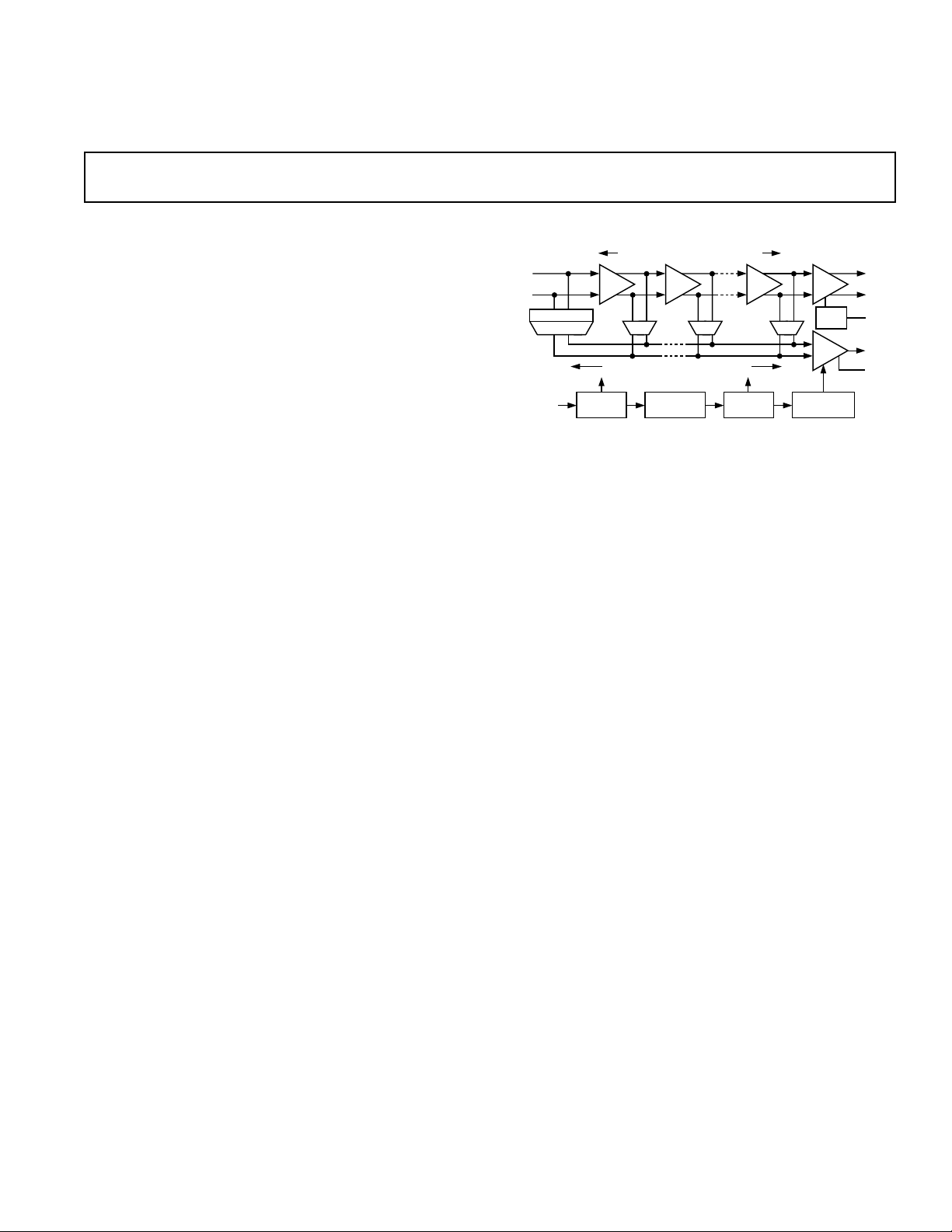
FUNCTIONAL BLOCK DIAGRAM
SIX STAGES TOTAL GAIN 72dB TYP GAIN 18dB
12dB
TEN DETECTORS SPACED 12dB
GAIN
BIAS
DET DET4 3 DET
BAND-GAP
REFERENCE
12dB
12dB LIM
DET
SLOPE
BIAS
INTERCEPT
TEMP COMP
BIAS
CTRL
I-V
LMHI
LMLO
LMDR
VLOG
FLTR
PRODUCT DESCRIPTION
The AD8309 is a complete IF limiting amplifier, providing both
an accurate logarithmic (decibel) measure of the input signal
(the RSSI function) over a dynamic range of 100 dB, and a
programmable limiter output, useful from 5 MHz to 500 MHz.
It is easy to use, requiring few external components. A single
supply voltage of +2.7 V to +6.5 V at 16 mA is needed, corresponding to a power consumption of under 50 mW at 3 V, plus
the limiter bias current, determined by the application and
typically 2 mA, providing a limiter gain of 100 dB when using
200 Ω loads. A CMOS-compatible control interface can enable
the AD8309 within about 500 ns and disable it to a standby
current of under 1 µA.
The six cascaded amplifier/limiter cells in the main path have a
small signal gain of 12.04 dB (×4), with a –3 dB bandwidth of
850 MHz, providing a total gain of 72 dB. The programmable
output stage provides a further 18 dB of gain. The input is fully
differential and presents a moderately high impedance (1 kΩ in
parallel with 2.5 pF). The input-referred noise-spectral-density,
when driven from a terminated 50 Ω, source is 1.28 nV/√Hz,
equivalent to a noise figure of 3 dB. The sensitivity of the
AD8309 can be raised by using an input matching network.
Each of the main gain cells includes a full-wave detector. An
additional four detectors, driven by a broadband attenuator, are
used to extend the top end of the dynamic range by over 48 dB.
The overall dynamic range for this combination extends from
–91 dBV (–78 dBm at the 50 Ω level) to a maximum permissible
value of +9 dBV, using a balanced drive of antiphase inputs each
of 2 V in amplitude, which would correspond to a sine wave
power of +22 dBm if the differential input were terminated in
50 Ω. The slope of the RSSI output is closely controlled to
20 mV/dB, while the intercept is set to –108 dBV (–95 dBm
re 50 Ω). These scaling parameters are determined by a band-
gap voltage reference and are substantially independent of temperature and supply. The logarithmic law conformance is typically
within ±0.4 dB over the central 80 dB of this range at any fre-
quency between 10 MHz and 200 MHz, and is degraded only
slightly at 500 MHz.
The RSSI response time is nominally 67 ns (10%–90%). The
averaging time may be increased without limit by the addition of
an external capacitor. The full output of 2.34 V at the maximum
input of +9 dBV can drive any resistive load down to 50 Ω and
this interface remains stable with any value of capacitance on
the output.
The AD8309 is fabricated on an advanced complementary
bipolar process using silicon-on-insulator isolation techniques
and is available in the industrial temperature range of –40°C to
+85°C, in a 16-lead TSSOP package.
REV. B
Information furnished by Analog Devices is believed to be accurate and
reliable. However, no responsibility is assumed by Analog Devices for its
use, nor for any infringements of patents or other rights of third parties
which may result from its use. No license is granted by implication or
otherwise under any patent or patent rights of Analog Devices.
One Technology Way, P.O. Box 9106, Norwood, MA 02062-9106, U.S.A.
Tel: 781/329-4700 World Wide Web Site: http://www.analog.com
Fax: 781/326-8703 © Analog Devices, Inc., 1999
Page 2

AD8309–SPECIFICATIONS
Parameter Conditions Min
INPUT STAGE (Inputs INHI, INLO)
Maximum Input
2
Differential Drive, p-p ±3.5 ±4V
(VS = +5 V, TA = +25ⴗC, unless otherwise noted)
1
Typ Max1Units
+9 dBV
Equivalent Power in 50 Ω Terminated in 52.3 Ω +22 dBm
Noise Floor Terminated 50 Ω Source 1.28 nV/√Hz
Equivalent Power in 50 Ω 500 MHz Bandwidth –78 dBm
Input Resistance From INHI to INLO 800 1000 1200 Ω
Input Capacitance From INHI to INLO 2.5 pF
DC Bias Voltage Either Input 1.725 V
LIMITING AMPLIFIER (Outputs LMHI, LMLO)
Usable Frequency Range 5 500 MHz
= R
At Limiter Output R
LOAD
= 50 Ω to –10 dB Point 875 MHz
LIM
Phase Variation at 100 MHz Over Input Range –60 dBm to +10 dBm ±3 Degrees
Limiter Output Current Nominally 400 mV/R
Versus Temperature –40°C ≤ T
Input Range
3
LIM
≤ +85°C –0.008 %/°C
A
0110mA
–78 +9 dBV
Equivalent dBm –65 +22 dBm
Maximum Output Voltage At Either LMHI or LMLO, wrt VPS2 1 1.25 V
Rise/Fall Time (10%–90%) R
≤ 50 Ω, 40 Ω ≤ R
LOAD
≤ 400 Ω 0.4 ns
LIM
LOGARITHMIC AMPLIFIER (Output VLOG)
±3 dB Error Dynamic Range From Noise Floor to Maximum Input 100 dB
Transfer Slope 5 MHz ≤ f ≤ 200 MHz 18 20 22 mV/dB
Over Temperature –40°C < T
< +85°C 17 20 23 mV/dB
A
Intercept (Log Offset) 5 MHz ≤ f ≤ 200 MHz –116 –108 –100 dBV
Equivalent dBm (re 50 Ω) –103 –95 –87 dBm
Over Temperature –40°C ≤ T
≤ +85°C –117 –108 –99 dBV
A
Equivalent dBm (re 50 Ω) –104 –95 –86 dBm
Temperature Sensitivity –0.009 dB/°C
Linearity Error (Ripple) Input from –83 dBV (–70 dBm) to +7 dBV (+20 dBm) ±0.4 dB
Output Voltage Input = –91 dBV (–78 dBm) V
Input = +9 dBV (+22 dBm) V
Input = +9 dBV (+22 dBm) V
Minimum Load Resistance, R
L
= +5 V, +2.7 V 0.34 V
S
= +5 V 2.34 2.75 V
S
= +2.75 V 2.10 V
S
40 50 Ω
Maximum Sink Current To Ground 0.75 1.0 1.25 mA
Output Resistance 0.3 Ω
Small-Signal Bandwidth 3.5 MHz
Output Settling Time to 1% Large Scale Input, +3 dBV (+16 dBm),
≥␣ 50 Ω, CL ≤␣ 100 pF 120 220 ns
R
L
Rise/Fall Time (10%–90%) Large Scale Input, +3 dBV (+16 dBm),
R
≥␣ 50 Ω, CL ≤␣ 100 pF 67 100 ns
L
POWER INTERFACES
Supply Voltage, V
POS
2.7 5 6.5 V
Quiescent Current Zero-Signal, LMDR Open 13 16 20 mA
Over Temperature –40°C < T
Disable Current –40°C < T
Additional Bias for Limiter R
LIM
Logic Level to Enable Power HI Condition, –40°C < T
Input Current when HI 3 V at ENBL, –40°C < T
< +85°C 111623mA
A
< +85°C 0.01 4 µA
A
= 400 Ω (See Text) 1.4 1.6 mA
< +85°C 1.8 V
A
< +85°C4060µA
A
POS
V
Logic Level to Disable Power LO Condition, –40°C < TA < +85°C –0.5 1 V
NOTES
1
Minimum and maximum specified limits on parameters that are guaranteed but not tested are six sigma values.
2
The input level is specified in “dBV” since logarithmic amplifiers respond strictly to voltage, not power. 0 dBV corresponds to a sinusoidal single-frequency input of
1 V rms. A power level of 0 dBm (1 mW) in a 50 Ω termination corresponds to an input of 0.2236 V rms. Hence, the relationship between dBV and dBm is a fixed
offset of +13 dBm in the special case of a 50 Ω termination.
3
Due to the extremely high Gain Bandwidth Product of the AD8309, the output of either LMHI or LMLO will be unstable for levels below –78 dBV (–65 dBm, re 50 Ω).
Specifications subject to change without notice.
–2–
REV. B
Page 3
AD8309
WARNING!
ESD SENSITIVE DEVICE
ABSOLUTE MAXIMUM RATINGS*
Supply Voltage VS . . . . . . . . . . . . . . . . . . . . . . . . . . . . . . 7.5 V
Input Level, Differential (re 50 Ω) . . . . . . . . . . . . . . . +26 dBm
Input Level, Single-Ended (re 50 Ω) . . . . . . . . . . . . . +20 dBm
Internal Power Dissipation . . . . . . . . . . . . . . . . . . . . . 500 mW
. . . . . . . . . . . . . . . . . . . . . . . . . . . . . . . . . . . . . . . 150°C/W
θ
JA
θ
. . . . . . . . . . . . . . . . . . . . . . . . . . . . . . . . . . . . . . .27.6°C/W
JC
Maximum Junction Temperature . . . . . . . . . . . . . . . . +125°C
Operating Temperature Range . . . . . . . . . . . . –40°C to +85°C
Storage Temperature Range . . . . . . . . . . . . . –65°C to +150°C
Lead Temperature Range (Soldering 60 sec) . . . . . . . . +300°C
*Stresses above those listed under Absolute Maximum Ratings may cause perma-
nent damage to the device. This is a stress rating only; functional operation of the
device at these or any other conditions above those indicated in the operational
section of this specification is not implied. Exposure to absolute maximum rating
conditions for extended periods may effect device reliability.
ORDERING GUIDE
Temperature Package Package
Model Range Description Option
AD8309ARU –40°C to +85°C 16-Lead TSSOP RU-16
AD8309ARU-REEL –40°C to +85°C 13" Tape and Reel RU-16
AD8309ARU-REEL7 –40°C to +85°C 7" Tape and Reel RU-16
AD8309-EVAL Evaluation Board
CAUTION
ESD (electrostatic discharge) sensitive device. Electrostatic charges as high as 4000 V readily
accumulate on the human body and test equipment and can discharge without detection.
Although the AD8309 features proprietary ESD protection circuitry, permanent damage may
occur on devices subjected to high energy electrostatic discharges. Therefore, proper ESD
precautions are recommended to avoid performance degradation or loss of functionality.
PIN FUNCTION DESCRIPTIONS
Pin Name Function
1 COM2 Special Common Pin for RSSI Output.
2 VPS1 Supply Pin for First Five Amplifier Stages
and the Main Biasing System.
3, 6, 11, 14 PADL Four Tie-Downs to the Paddle on Which
the IC Is Mounted; Grounded.
4 INHI Signal Input, HI or Plus Polarity.
5 INLO Signal Input, LO or Minus Polarity.
7 COM1 Main Common Connection.
8 ENBL Chip Enable; Active When HI.
9 LMDR Limiter Drive Programming Pin.
10 FLTR RSSI Bandwidth-Reduction Pin.
12 LMLO Limiter Output, LO or Minus Polarity.
13 LMHI Limiter Output, HI or Plus Polarity.
15 VPS2 Supply Pin for Sixth Gain Stage, Limiter
and RSSI Output Stage Load Current.
16 VLOG Logarithmic (RSSI) Output.
PIN CONFIGURATION
COM2
VPS1
PADL
INHI
INLO
PADL
COM1
ENBL
1
2
3
AD8309
4
TOP VIEW
5
(Not to Scale)
6
7
8
16
VLOG
VPS2
15
PADL
14
LMHI
13
LMLO
12
PADL
11
FLTR
10
LMDR
9
REV. B
–3–
Page 4
AD8309–Typical Performance Characteristics
100
10
1
0.1
0.01
0.001
SUPPLY CURRENT – mA
0.0001
0.00001
0.5 2.50.7
+258C
+858C
–408C
0.9 1.1 1.3 1.5 1.7 1.9 2.1 2.3
ENABLE VOLTAGE – V
Figure 1. Supply Current vs. Enable Voltage @
T
= –40°C, +25°C and +85°C
A
–13dBV
–33dBV
–53dBV
–73dBV
–93dBV
VLOG
500mV PER
VERTICAL
DIVISION
GROUND REFERENCE
5V PER
VERTICAL
DIVISION
ENBL
500ns PER HORIZONTAL
DIVISION
VLOG
500mV PER
VERTICAL
DIVISION
GROUND REFERENCE
+10dBm INPUT
LEVEL SHOWN
HERE
100ns PER HORIZONTAL
DIVISION
500mV PER
VERTICAL DIVISION
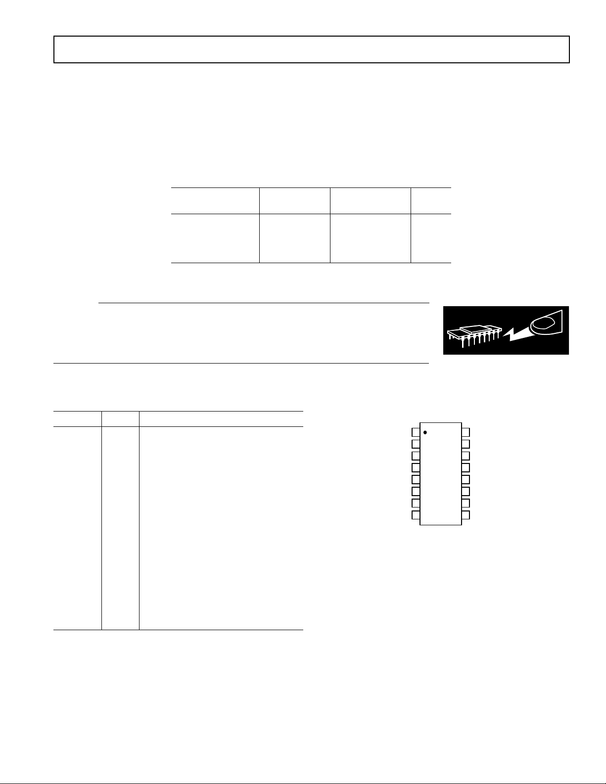
Figure 4. RSSI Pulse Response for Inputs Stepped from
Zero to –63 dBV, –43 dBV, –23 dBV, –3 dBV
VLOG
500mV PER
VERTICAL
DIVISION
GROUND REFERENCE
INPUT
1V PER VERTICAL
100ns PER HORIZONTAL
DIVISION
DIVISION
Figure 2. Power On/Off Response Time with RF Input of
–93 dBV to –13 dBV
VLOG
500mV PER
VERTICAL DIVISION
GROUND REFERENCE
INPUT
500mV PER
VERTICAL DIVISION
200ns PER HORIZONTAL
DIVISION
Figure 3. Large Signal RSSI Pulse Response with
C
= 100 pF and RL = 50Ω and 75Ω (Curves Overlap)
L
Figure 5. Large Signal RSSI Pulse Response with RL = 100
and CL = 33 pF, 100 pF and 330 pF (Curves Overlap)
27pF
VLOG
200mV PER
VERTICAL DIVISION
GROUND REFERENCE
270pF
3300pF
100ms PER
HORIZONTAL
DIVISION
Figure 6. Small Signal AC Response of RSSI Output with
External Filter Capacitance of 27 pF, 270 pF and 3300 pF
Ω
–4–
REV. B
Page 5
AD8309
2.5
2.0
1.5
1.0
RSSI OUTPUT – V
TA = +858C
0.5
TA = –408C
–80 –60 –40 –20 0 20 40
INPUT LEVEL – dBm Re 50V
0
–100
TA = +258C
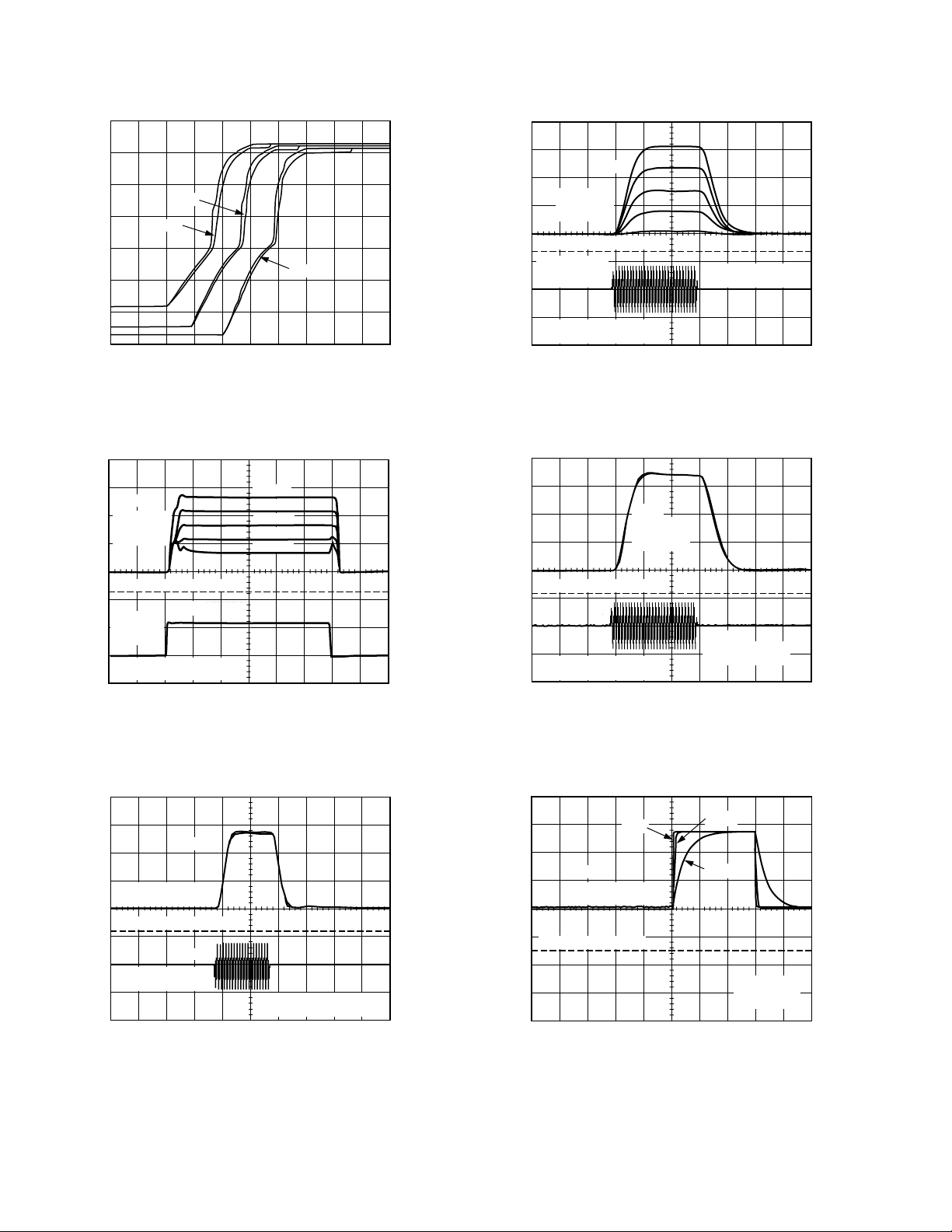
Figure 7. RSSI Output vs. Input Level, 100 MHz Sine Input,
= –40°C, +25°C and +85°C, Single-Ended Input
at T
A
2.5
2.0
1.5
1.0
RSSI OUTPUT – V
0.5
0
–80 –60 –40 –20 0 20 40
–100
INPUT LEVEL – dBm Re 50V
100MHz
50MHz
200MHz
5MHz
Figure 8. RSSI Output vs. Input Level, at TA = +25°C, for
Frequencies of 5 MHz, 50 MHz, 100 MHz and 200 MHz
5
4
3
2
TA = +258C
TA = –408C
0
TA = +858C
20 40
1
0
–1
ERROR – dB
–2
–3
–4
–5
–100
–80 –60 –40 –20
INPUT LEVEL – dBm Re 50V
Figure 10. Log Linearity of RSSI Output vs. Input Level,
100 MHz Sine Input, at T
5
4
3
2
1
0
–1
ERROR – dB
–2
–3
–4
–5
–90
5MHz
50MHz
100MHz
–80 –70 –60 –50
= –40°C, +25°C, and +85°C
A
DYNAMIC RANGE
5MHz
50MHz
100MHz
200MHz
200MHz
–40 –30 –20 –10 0 10 20 30
INPUT LEVEL – dBm Re 50V
61dB
85
91
97
96
63dB
93
99
103
102
Figure 11. Log Linearity of RSSI Output vs. Input Level, at
T
= +25°C, for Frequencies of 5 MHz, 50 MHz, 100 MHz
A
and 200 MHz
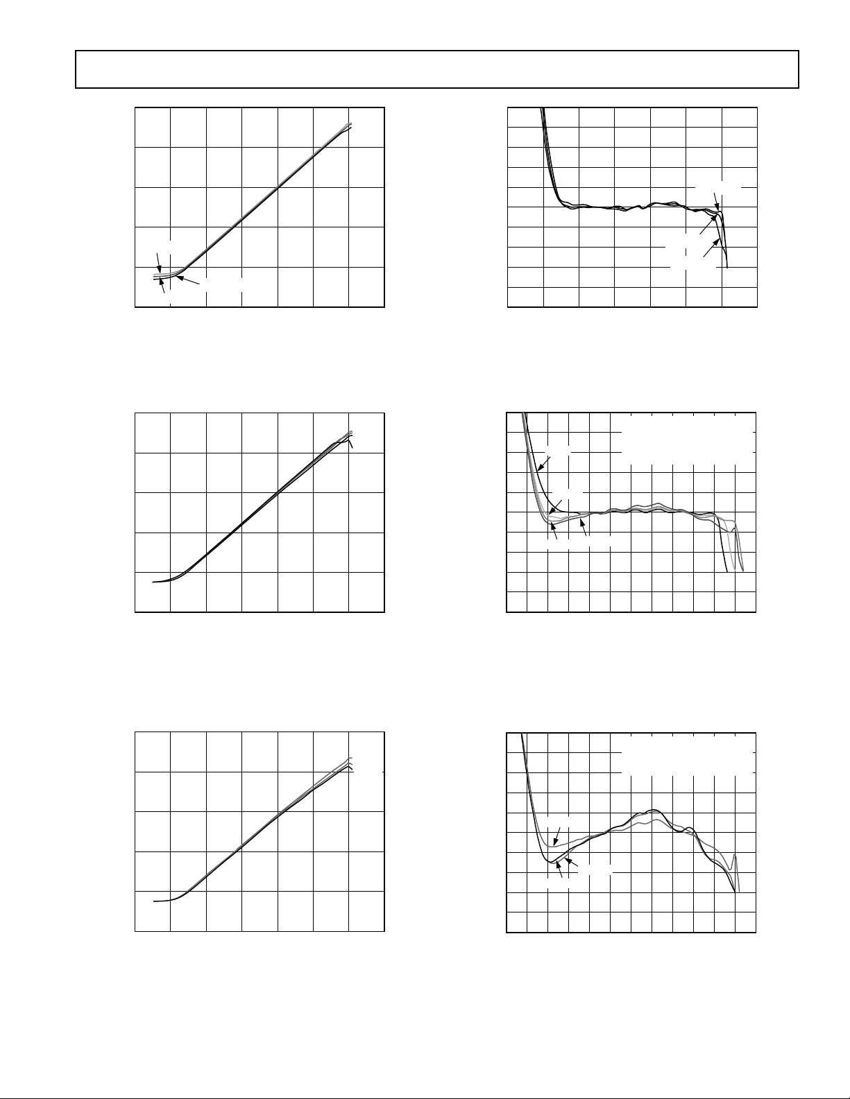
2.5
300MHz
400MHz
2.0
1.5
1.0
RSSI OUTPUT – V
0.5
0
–80 –60 –40 –20 0 20 40
–100
INPUT LEVEL – dBm Re 50V
500MHz
Figure 9. RSSI Output vs. Input Level, at TA = +25°C, for
Frequencies of 300 MHz, 400 MHz and 500 MHz
REV. B
5
4
3
2
1
0
–1
ERROR – dB
–2
–3
–4
–5
–90
300MHz
400MHz
500MHz
–80 –70 –60 –50 –40 –30 –20 –10 0 10 20 30
INPUT LEVEL – dBm Re 50V
DYNAMIC RANGE
300MHz
400MHz
500MHz
61dB
90
65
66
63dB
102
100
100
Figure 12. Log Linearity of RSSI Output vs. Input Level,
at T
= +25°C, for Frequencies of 300 MHz, 400 MHz and
A
500 MHz
–5–
Page 6
AD8309
25
24
23
22
21
20
19
RSSI SLOPE – mV/dB
18
17
16
15
1
10 100 1000
FREQUENCY – MHz
Figure 13. RSSI Slope vs. Frequency Using Termination of
Ω
in Series with 4.7 nH
52.3
2ns PER HORIZONTAL DIVISION
LIMITER OUTPUTS 100mV PER VERTICAL DIVISION
–103
–104
–105
–106
–107
–108
–109
–110
RSSI INTERCEPT – dBV
–111
–112
–113
1
10 100 1000
FREQUENCY – MHz
Figure 16. RSSI Intercept vs. Frequency Using Termina-
Ω
tion of 52.3
in Series with 4.7 nH
14
12
10
ADDITIONAL SUPPLY CURRENT
8
2mV PER VERTICAL DIVISION
Figure 14. Limiter Output at 300 MHz for a Sine Wave
Input of –60 dBV (–47 dBm), Using an R
R
LIM
of 100
Ω
LMLO
LMHI
LIMITER OUTPUTS
50mV PER VERTICAL DIVISION
INPUT
1mV PER VERTICAL DIVISION
12.5ns PER HORIZONTAL
of 50 Ω and an
LOAD
DIVISION
Figure 15. Limiter Response at LMHI, LMLO with Pulsed
Sine Input of –70 dBV (–57 dBm) at 50 MHz; R
= 200
R
LIM
Ω
LOAD
= 50 Ω,
6
CURRENT – mA
4
2
LIMITER OUTPUT CURRENT
0
0
100 200 300 400 450
150 250 35050
R
– V
LIM
Figure 17. Additional Supply Current and Limiter Output Current vs. R
10
8
6
TA = +858C
4
2
0
–2
NORMALIZED
TA = +258C
–4
–6
LIMITER PHASE RESPONSE – Degrees
–8
–10
–60
LIM
TA = –408C
–50 –30 –20 –10 10
–40 0
INPUT LEVEL – dBm Re 50V
Figure 18. Normalized Limiter Phase Response vs. Input
Level. Frequency = 100 MHz; T
= –40°C, +25°C and +85°C
A
–6–
REV. B
Page 7

AD8309
THEORY OF OPERATION
The AD8309 is an advanced IF signal processing IC, intended
for use in high performance receivers, combining two key functions. First, it provides a large voltage gain combined with progressive compression, through which an IF signal of high dynamic
range is converted into a square-wave (that is, hard limited)
output, from which frequency and phase information modulated
on this input can be recovered by subsequent signal processing.
For this purpose, the noise level referred to the input must be
very low, since it determines the detection threshold for the receiver.
Further, it is often important that the group delay in this amplifier be essentially independent of the signal level, to minimize
the risk of amplitude-to-phase conversion. Finally, it is also desirable that the amplitude of the limited output be well defined and
temperature stable. In the AD8309, this amplitude can be controlled by the user, or even completely shut off, providing greater
flexibility.
The second function is to provide a demodulated (baseband)
output proportional to the decibel value of the signal input,
which may be used to measure the signal strength. This output,
which typically runs from a value close to the ground level to a
few volts above ground, is called the Received Signal Strength
Indication, or RSSI. The provision of this function requires the
use of a logarithmic amplifier (log amp). For this output to be
suitable for measuring signal strength, it is important that its
scaling attributes are well controlled.
These are the logarithmic slope, specified in mV/dB, and the
intercept, often specified as an equivalent power level at the
amplifier input, although a log amp is inherently a voltageresponding device. (See further discussion, below). Also
important is the law conformance, that is, how well the RSSI
approximates an ideal function. Many low quality log amps
provide only an approximate solution, resulting in large errors in
law conformance and scaling. All Analog Devices log amps are
designed with close attention to matters affecting accuracy of
the overall function.
In the AD8309, these two basic signal-processing functions are
combined to provide the necessary voltage gain with progressive
compression and hard limiting, and the determination of the
logarithmic magnitude of the input (RSSI). This combination is
called a log limiting amplifier. A good grasp of how this product
works will avoid many pitfalls in their application.
Log-Amp Fundamentals
The essential purpose of a logarithmic amplifier is to reduce a
signal of wide dynamic range to its decibel equivalent. It is thus
primarily a measurement device. The logarithmic representation
leads to situations that may be confusing or even paradoxical.
For example, a voltage offset added to the RSSI output of a log
amp is equivalent to a gain increase ahead of its input.
When all the variables expressed as voltages, then, regardless of
the particular structure, the output can be expressed as
V
OUT
where V
= VY log (V
is the “slope voltage.” VIN is the input voltage, and V
Y
) (1)
IN /VX
X
is the “intercept voltage.” The logarithm is usually to base-10,
which is appropriate to a decibel-calibrated device, in which
case V
(1) that a log amp requires two references, here V
is also the “volts-per-decade.” It will be apparent from
Y
and VY, that
X
determine the scaling of the circuit. The absolute accuracy of a
log amp cannot be any better than the accuracy of its scaling
references. Note that (1) is mathematically incomplete in representing the behavior of a demodulating log amp such as the
AD8309, where V
has an alternating sign. However, the basic
IN
principles are unaffected.
Figure 19 shows the input/output relationship of an ideal log
amp, conforming to Equation (1). The horizontal scale is logarithmic, and spans a very wide dynamic range, shown here as
over 120 dB, that is, six decades of voltage or twelve decades of
input-referred power. The output passes through zero (the
“log-intercept”) at the unique value V
= VX and becomes
IN
negative for inputs below the intercept. In the ideal case, the
straight line describing V
for all values of VIN would con-
OUT
tinue indefinitely in both directions. The dotted line shows that
the effect of adding an offset voltage V
lower the effective intercept voltage V
V
OUT
5V
Y
4V
V
OUT
Y
3V
Y
2V
Y
V
Y
= 0
VIN = 10–2V
–40dBc
–2V
Y
LOWER INTERCEPT
VIN = V
X
0dBc
X
V
IN
+40dBc
V
SHIFT
= 102V
to the output is to
SHIFT
.
X
= 104V
V
X
IN
+80dBc
X
LOG V
IN
Figure 19. Ideal Log Amp Function
Exactly the same modification could be achieved raising the gain
(or signal level) ahead of the log amp by the factor V
For example, if V
is 400 mV/decade (that is, 20 mV/dB, as for
Y
SHIFT/VY
.
the AD8309), an offset of 120 mV added to the output will
appear to lower the intercept by two tenths of a decade, or 6 dB.
Adding an offset to the output is thus indistinguishable from
applying an input level that is 6 dB higher.
The log amp function described by (1) differs from that of a
linear amplifier in that the incremental gain DV
very strong function of the instantaneous value of V
/DVIN is a
OUT
IN
, as is
apparent by calculating the derivative. For the case where the
logarithmic base is e, it is easy to show that
∆
V
OUTINY
∆
VVV
=
IN
(2)
That is, the incremental gain of a log amp is inversely proportional to the instantaneous value of the input voltage. This remains true for any logarithmic base. A “perfect” log amp would
be required to have infinite gain under classical “small-signal”
(zero-amplitude) conditions. This demonstrates that, whatever
means might be used to implement a log amp, accurate HF
response under small signal conditions (that is, at the lower end
of the full dynamic range) demands the provision of a very high
gain-bandwidth product. A wideband log amp must therefore use
many cascaded gain cells each of low gain but high bandwidth.
For the AD8309, the gain-bandwidth (–10 dB) product is
52,500 GHz.
REV. B
–7–
Page 8

AD8309
As a consequence of this high gain, even very small amounts of
thermal noise at the input of a log amp will cause a finite output
for zero input, resulting in the response line curving away from
the ideal (Figure 19) at small inputs, toward a fixed baseline.
This can either be above or below the intercept, depending on
the design. Note that the value specified for this intercept is
invariably an extrapolated one: the RSSI output voltage will never
attain a value of exactly zero in a single supply implementation.
Voltage (dBV) and Power (dBm) Response
While Equation 1 is fundamentally correct, a simpler formula is
appropriate for specifying the RSSI calibration attributes of a
log amp like the AD8309, which demodulates an RF input. The
usual measure is input power:
V
= V
OUT
V
is the demodulated and filtered RSSI output, V
OUT
SLOPE (PIN
logarithmic slope, expressed in volts/dB, P
– P0 ) (3)
is the
is the input power,
IN
SLOPE
expressed in decibels relative to some reference power level and
P
is the logarithmic intercept, expressed in decibels relative to
0
the same reference level.
The most widely used convention in RF systems is to specify
power in decibels above 1 mW in 50 Ω, written dBm. (However,
that the quantity [P
– P0 ] is simply dB). The logarithmic
IN
function disappears from this formula because the conversion
has already been implicitly performed in stating the input in
decibels.
Specification of log amp input level in terms of power is strictly
a concession to popular convention: they do not respond to
power (tacitly “power absorbed at the input”), but to the input
voltage. In this connection, note that the input impedance of the
AD8309 is much higher that 50 Ω, allowing the use of an im-
pedance transformer at the input to raise the sensitivity, by up
to 13 dB.
The use of dBV, defined as decibels with respect to a 1 V rms sine
amplitude, is more precise, although this is still not unambiguous
complete as a general metric, because waveform is also involved
in the response of a log amp, which, for a complex input (such
as a CDMA signal) will not follow the rms value exactly. Since
most users specify RF signals in terms of power—more specifi-
cally, in dBm/50 Ω—we use both dBV and dBm in specifying
the performance of the AD8309, showing equivalent dBm levels
for the special case of a 50 Ω environment.
Progressive Compression
High speed, high dynamic range log amps use a cascade of
nonlinear amplifier cells (Figure 20) to generate the logarithmic
function from a series of contiguous segments, a type of piecewise-linear technique. This basic topology offers enormous gainbandwidth products. For example, the AD8309 employs in its
main signal path six cells each having a small-signal gain of
12.04 dB (×4) and a –3 dB bandwidth of 850 MHz, followed by
a final limiter stage whose gain is typically 18 dB. The overall
gain is thus 100,000 (100 dB) and the bandwidth to –10 dB
point at the limiter output is 525 MHz. This very high gainbandwidth product (52,500 GHz) is an essential prerequisite to
accurate operation under small signal conditions and at high
frequencies: Equation (2) reminds us that the incremental gain
decreases rapidly as V
increases. The AD8309 exhibits a loga-
IN
rithmic response over most of the range from the noise floor of
–91 dBV, or 28 µV rms, (or –78 dBm/50 Ω) to a breakdown-
limited peak input of 4 V (requiring a balanced drive at the
differential inputs INHI and INLO).
–8–
STAGE 1 STAGE 2 STAGE N –1 STAGE N
V
A
X
A A A
V
W
Figure 20. Cascade of Nonlinear Gain Cells
Theory of Logarithmic Amplifiers
To develop the theory, we will first consider a somewhat different scheme to that employed in the AD8309, but which is simpler to explain, and mathematically more straightforward to
analyze. This approach is based on a nonlinear amplifier unit,
which we may call an A/1 cell, having the transfer characteristic
shown in Figure 21. We here use lowercase variables to define
the local inputs and outputs of these cells, reserving uppercase
for external signals.
The small signal gain ∆V
inputs up to the knee voltage E
OUT
/∆V
is A, and is maintained for
IN
, above which the incremental
K
gain drops to unity. The function is symmetrical: the same drop
in gain occurs for instantaneous values of V
less than –EK.
IN
The large signal gain has a value of A for inputs in the range
< VIN < +EK, but falls asymptotically toward unity for very
–E
K
large inputs.
In logarithmic amplifiers based on this simple function, both the
slope voltage and the intercept voltage must be traceable to the
one reference voltage, E
. Therefore, in this fundamental analy-
K
sis, the calibration accuracy of the log amp is dependent solely on
this voltage. In practice, it is possible to separate the basic references used to determine V
able to an on-chip band-gap reference, while V
and VX. In the AD8309, VY is trace-
Y
is derived from
X
the thermal voltage kT/q and later temperature-corrected by a
precise means.
Let the input of an N-cell cascade be V
V
. For small signals, the overall gain is simply AN. A six-
OUT
, and the final output
IN
stage system in which A = 5 (14 dB) has an overall gain of
15,625 (84 dB). The importance of a very high small-signal ac
gain in implementing the logarithmic function has already been
noted. However, this is a parameter of only incidental interest in
the design of log amps; greater emphasis needs to be placed on
the nonlinear behavior.
A/1
K
OUTPUT
0
E
K
SLOPE = 1
SLOPE = A
INPUT
AE
Figure 21. The A/1 Amplifier Function
Thus, rather than considering gain, we will analyze the overall
nonlinear behavior of the cascade in response to a simple dc
input, corresponding to the V
inputs, the output from the first cell is V
second, V
value of V
the knee voltage E
cells of gain A ahead of this node, we can calculate that V
E
/A
K
= A2 VIN, and so on, up to VN = AN VIN. At a certain
2
, the input to the Nth cell, V
IN
N–1
. This unique point corresponds to the lin-log transition,
. Thus, V
K
of Equation (1). For very small
IN
= AEK and since there are N–1
OUT
= AVIN; from the
1
, is exactly equal to
N–1
IN
=
REV. B
Page 9

labeled ① on Figure 22. Below this input, the cascade of gain
cells is acting as a simple linear amplifier, while for higher values
of V
, it enters into a series of segments which lie on a logarith-
IN
mic approximation.
Continuing this analysis, we find that the next transition occurs
when the input to the (N–1)th stage just reaches E
when V
AE
IN
. It is easily demonstrated (from the function shown in
K
= EK /A
N–2
. The output of this stage is then exactly
Figure 21) that the output of the final stage is (2A–1)E
beled ≠ on Figure 22). Thus, the output has changed by an
amount (A–1)E
for a change in VIN from EK /A
K
, that is,
K
N–1
to EK /A
K
(la-
N–2
,
that is, a ratio change of A.
V
OUT
(4A-3) E
K
(3A-2) E
(2A-1) E
AE
K
K
K
0
(A-1) E
K
RATIO
OF A
N–1
E
/A
K
EK/A
N–2
EK/A
N–3
EK/A
N–4
LOG V
IN
Figure 22. The First Three Transitions
At the next critical point, labeled ③, the input is A times larger
and V
increment of (A–1)E
has increased to (3A–2)EK, that is, by another linear
OUT
. Further analysis shows that, right up to
K
the point where the input to the first cell reaches the knee voltage, V
Expressed as a certain fraction of a decade, this is simply log
changes by (A–1)EK for a ratio change of A in VIN.
OUT
10
(A).
For example, when A = 5 a transition in the piecewise linear
output function occurs at regular intervals of 0.7 decade (log10(A),
or 14 dB divided by 20 dB). This insight allows us to immediately state the “Volts per Decade” scaling parameter, which is
also the “Scaling Voltage” V
Linear Change inV
V
==
Y
Decades Change inV
when using base-10 logarithms:
Y
AE
( –)
OUT
IN
1
A
log ( )
10
K
(4)
Note that only two design parameters are involved in determining V
, namely, the cell gain A and the knee voltage EK, while
Y
N, the number of stages, is unimportant in setting the slope of
the overall function. For A = 5 and E
= 100 mV, the slope
K
would be a rather awkward 572.3 mV per decade (28.6 mV/dB).
A well designed practical log amp will provide more rational
scaling parameters.
The intercept voltage can be determined by solving Equation
(4) for any two pairs of transition points on the output function
(see Figure 22). The result is:
E
=
A
K
+(/[–])11
NA
evaluates
X
(5)
V
X
For the example under consideration, using N = 6, V
to 4.28 µV, which thus far in this analysis is still a simple dc
voltage.
AD8309
SLOPE = 0
AE
K
A/0
OUTPUT
0
Figure 23. A/0 Amplifier Functions (Ideal and tanh)
Care is needed in the interpretation of this parameter. It was
earlier defined as the input voltage at which the output passes
through zero (see Figure 19). Clearly, in the absence of noise
and offsets, the output of the amplifier chain shown in Figure 20
can only be zero when V
= 0. This anomaly is due to the finite
IN
gain of the cascaded amplifier, which results in a failure to maintain the logarithmic approximation below the “lin-log transition”
(Point ① in Figure 22). Closer analysis shows that the voltage
given by Equation (5) represents the extrapolated, rather than
actual, intercept.
Demodulating Log Amps
Log amps based on a cascade of A/1 cells are useful in baseband
(pulse) applications, because they do not demodulate their input
signal. Demodulating (detecting) log-limiting amplifiers such as
the AD8309 use a different type of amplifier stage, which we
will call an A/0 cell. Its function differs from that of the A/1 cell
in that the gain above the knee voltage E
by the solid line in Figure 23. This is also known as the limiter
function, and a chain of N such cells is often used alone to
generate a hard limited output, in recovering the signal in FM
and PM modes.
The AD640, AD606, AD608, AD8307, AD8309, AD8313 and
other Analog Devices communications products incorporating a
logarithmic IF amplifier all use this technique. It will be apparent that the output of the last stage cannot now provide a logarithmic output, since this remains unchanged for all inputs
above the limiting threshold, which occurs at VIN = EK /A
Instead, the logarithmic output is generated by summing the
outputs of all the stages. The full analysis for this type of log amp
is only slightly more complicated than that of the previous case.
It can be shown that, for practical purpose, the intercept voltage
V
is identical to that given in Equation (5), while the slope
X
voltage is:
AE
=
log ( )
K
A
10
V
Y
An A/0 cell can be very simple. In the AD8309 it is based on a
bipolar-transistor differential pair, having resistive loads R
an emitter current source I
. This amplifier limiter cell exhibits
E
an equivalent knee-voltage of E
gain of A = I
. The large signal transfer function is the
ERL /EK
hyperbolic tangent (see dotted line in Figure 23). This function
is very precise, and the deviation from an ideal A/0 form is not
detrimental. In fact, the “rounded shoulders” of the tanh function beneficially result in a lower ripple in the logarithmic conformance than that which would be obtained using an ideal A/0
function. A practical amplifier chain built of these cells is differential in structure from input to final output, and has a low
SLOPE = A
E
K
= 2kT/q and a small-signal
K
INPUT
falls to zero, as shown
K
N–1
L
.
(6)
and
REV. B
–9–
Page 10

AD8309
sensitivity to disturbances on the supply lines. With careful
design, the sensitivities to many other parametric variations, and
the effects of temperature and supply voltage, can be reduced to
negligible proportions.
STAGE 1 STAGE 2 STAGE N
V
IN
g
m
+TOP-END
DETECTORS
A/0 A/0 A/0
g
m
CURRENT-SUMMING LINE
g
m
g
m
–
R
SLOPE
V
LIM
V
LOG
Figure 24. Basic Log Amp Structure Using A/0 Stages and
Transconductance (g
) Cells for Summing
m
The output of each gain cell has an associated transconductance
(g
) cell, which converts the differential output voltage of the
m
cell to a pair of differential currents; these are summed by simply connecting the outputs of all the g
(detector) stages in
m
parallel. The total current is then converted back to a voltage by
a transresistance stage, which determines the slope of the logarithmic output. This general scheme is depicted, in a simplified
single-sided form, in Figure 24. Additional detectors, driven by
a passive attenuator, may be added to extend the top end of the
dynamic range.
The slope voltage may now be decoupled from the knee-voltage
E
= 2kT/q, which is inherently PTAT. The detector stages are
K
biased with currents (not shown in the Figure) which can be
derived from a band-gap reference and thus be stable with temperature. This is the architecture used in the AD8309. It affords
complete control over the magnitude and temperature behavior
of the logarithmic slope.
A further step is yet needed to achieve the demodulation response,
required in a log-limiter amp is to convert an alternating input
into a quasi- dc baseband output. This is achieved by modifying
cells used for summation purposes to implement the
the g
m
rectification function. Early log amps based on the progressive
compression technique used half-wave rectifiers, which made
post-detection filtering difficult. The AD640 was the first commercial monolithic log amp to use a full-wave rectifier; this
proprietary practice has been used in all subsequent Analog
Devices types.
We can model these detectors as being essentially linear g
cells,
m
but producing an output current that is independent of the sign
of the voltage applied to the input. That is, they implement the
absolute-value function. Since the output from the later A/0 stages
closely approximates an amplitude symmetric square wave for
even moderate input levels, the current output from each detector is almost constant over each period of the input. Somewhat
earlier detectors stages in the chain produce a waveform having
only very brief “dropouts” at twice the input frequency. Only
those detectors nearest the log amp’s input produce a low level
waveform that is approximately sinusoidal. When all these (current mode) outputs are summed, the resulting signal has a waveform which is readily filtered, to provide a low residual ripple on
the output.
Intercept Calibration
Monolithic log amps from Analog Devices incorporate accurate
means to position the intercept voltage V
(or equivalent sine-
X
wave power for a demodulating log amp, when driven at a specific impedance level). Using the scheme shown in Figure 24,
the value of the intercept level departs considerably from that
predicted by the simple theory. Nevertheless, the intrinsic intercept voltage is still proportional to E
, which is PTAT (propor-
K
tional to absolute temperature).
Recalling that the addition of an offset to the output produces
an effect which is indistinguishable from a change in the position of the intercept, it will be apparent that we can cancel the
“left-right” motion of V
tion of E
by simply adding an offset at its demodulated output
K
resulting from the temperature varia-
X
having the required temperature behavior.
The precise temperature-shaping of the intercept-positioning
offset can result in a log amp having stable scaling parameters,
making it a true measurement device, for example, as a calibrated
Received Signal Strength Indicator (RSSI). In this application,
one is more interested in the value of the output for an input
waveform which is often sinusoidal (CW). The input level be
stated as an equivalent power, in dBm, but it is essential to
know the impedance level at which this “power” is presumed to
be measured. In an impedance of 50 Ω, 0 dBm (1 mW) corre-
sponds to a sinusoidal amplitude of 316.2 mV (223.6 mV rms).
For the AD8309, the intercept may be specified in dBm when
the input impedance is lowered to 50 Ω, by the addition of a
shunt resistor of 52.3 Ω, in which case it occurs at –95 dBm.
However, the response is actually to the voltage at the input, not
the power in the termination resistor, and should be specified in
dBV. A –95 dBm sine input across a 50 Ω resistance corresponds to an amplitude of 5.6 µV, or –108 dBV, where 0 dBV is
specified as a sine waveform of 1 V rms, that is, 2.8 V p-p.
Note that a log amp’s intercept is a function of waveform. For
example, a square-wave input will read 6 dB
higher than a sinewave of the same amplitude, and a Gaussian noise input 0.5 dB
higher than a sine wave of the same rms value. Further, a log
amp driven by the sum of two sinusoidal voltages of equal amplitude will show an output that is only 2.1 dB higher than the
response for a single sine wave drive, rather than the 3 dB that
might be expected if the device truly responded to input power.
These are characteristics exhibited by all demodulating log amps.
Dynamic Range
The lower end of the dynamic range is determined largely by the
thermal noise floor, measured at the input of the amplifier chain.
For the AD8309, the short-circuit input-referred noise-spectral
density is 1.1 nV/√Hz, and 1.275 nV/√Hz when driven from a
net source impedance of 25 Ω (a terminated 50 Ω). This corre-
sponds to a noise power of –78 dBm in a 500 MHz bandwidth.
The upper end of the dynamic range is extended upward by the
addition of top-end detectors driven by a tapped attenuator. These
smaller signals are applied to additional full-wave detectors
whose outputs are summed with those of the main detectors.
With care in design, this extension in the dynamic range can be
‘seamless’ over the full frequency range. For the AD8309 it
amounts to a further 48 dB. When using a supply of 4.5 V or
greater, an input amplitude of 4 V can be accommodated, corre-
sponding to a power level of +22 dBm in 50 Ω. (A larger input
voltage may cause damage.)
–10–
REV. B
Page 11

AD8309
The total dynamic range of the AD8309, defined as the ratio
of the maximum permissible input to the noise floor, is thus
100 dB. Good accuracy is provided over a substantial part of
this range.
Input Matching
Monolithic log amps present a nominal input impedance much
higher than 50 Ω. For the AD8309, this can be modeled as 1 kΩ
shunted by 2.5 pF, at frequencies up to 300 MHz. Thus, a
simple input matching network can considerably improve the
basic sensitivity , when driving from a low-impedance source, by
increasing the voltage applied to the input. For a 50:1000 Ω
transformation, the voltage gain is 13 dB, and the whole dynamic range moves downward by this amount; that is, the inter-
cept is shifted to –121 dBV (–108 dBm at the primary 50 Ω
input). Note that while useful voltage gain is achieved in this
way, it does not follow that the noise-figure is minimal at the
optimum power match.
Offset Control
In a monolithic log amp, direct-coupling between the stages is
invariably utilized for practical reasons. Now, a dc offset voltage
in the early stages of the chain is indistinguishable from a “real”
signal. If as high as 400 µV, it would be 20 dB larger than the
smallest resolvable ac signal (40 µV), reducing the dynamic
range by this amount. This problem is solved by using a global
feedback path from the last stage to the first. The high-frequency
components of the signal must be removed; this achieved in the
AD8309 by an on-chip low-pass filter, providing sufficient suppression of HF feedback to allow accurate operation down to at
least 5 MHz. Useful operation at lower frequencies remains
possible, although a particular device having a large dc offset will
exhibit a reduction in the low end region of the dynamic range.
PRODUCT OVERVIEW
The AD8309 is built on an advanced dielectrically-isolated
complementary bipolar process using thin-film resistor technology for accurate scaling. It follows well-developed foundations
proven over a period of some fifteen years, with constant refinement. The backbone of the AD8309 (Figure 25) comprises a
chain of six main amplifier/limiter stages, each having a gain of
12.04 dB (×4) and small-signal –3 dB bandwidth of 850 MHz.
The input interface at INHI and INLO (Pins 4 and 5) is fully
differential. Thus it may be driven from either single-sided or
balanced inputs, the latter being required at the very top end of
the dynamic range, where the total differential drive may be as
large as 4 V in amplitude.
The first six stages, also used in developing the logarithmic
RSSI output, are followed by a versatile programmable output,
and thus programmable gain, final limiter section. Its opencollector outputs are also fully differential, at LMHI and LMLO
(Pins 12 and 13). This output stage provides a gain of 18 dB
when using equal valued load and bias setting resistors and the
pin-to-pin output is used. The overall voltage gain is thus 100 dB.
When using R
LIM
= R
= 200 Ω, the additional current
LOAD
consumption in the limiter is approximately 2.8 mA, of which
2 mA goes to the load. The ratio depends on R
(for example,
LIM
when 20 Ω, the efficiency is 90%), and the voltage at the pin
LMDR is rather more than 400 mV, but the total load current is
accurately (400 mV)/R
LIM
.
The rise and fall times of the hard-limited (essentially squarewave) voltage at the outputs are typically 0.4 ns, when driven by
a sine wave input having an amplitude of 100 mV or greater,
and R
= 50 Ω. The change in time-delay (“phase skew”)
LOAD
over the input range –83 dBV (100 mV in amplitude, or –70 dBm
in 50 Ω) to –3 dBV (1 V or +10 dBm) is ±83 ps (±3° at 100 MHz).
SIX STAGES TOTAL GAIN 72dB TYP GAIN 18dB
INHI
INLO
LADR ATTEN
ENBL
12dB
TEN DETECTORS SPACED 12dB
GAIN
BIAS
DET DET4 3 DET
BAND-GAP
REFERENCE
12dB
12dB LIM
DET
SLOPE
BIAS
BIAS
CTRL
I-V
INTERCEPT
TEMP COMP
LMHI
LMLO
LMDR
VLOG
FLTR
Figure 25. Main Features of the AD8309
The six main cells and their associated full-wave detectors,
having a transconductance (g
) form, handle the lower part of
m
the dynamic range. Biasing for these cells is provided by two
references, one of which determines their gain, the other being a
band-gap cell which determines the logarithmic slope, and stabilizes it against supply and temperature variations. A special dcoffset-sensing cell (not shown in Figure 25) is placed at the end
of this main section, and used to null any residual offset at the
input, ensuring accurate response down to the noise floor. The
first amplifier stage provides a short-circuited voltage-noise
spectral-density of 1.07 nV/√Hz.
The last detector stage includes a modification to temperaturestabilize the log-intercept, which is accurately positioned so as to
make optimal use of the full output voltage range. Four further
“top end” detectors are placed at 12.04 dB taps along a passive
attenuator, to handle the upper part of the range. The differential current-mode outputs of all ten detectors stages are summed
with equal weightings and converted to a single-sided voltage by
the output stage, generating the logarithmic (or RSSI) output at
VLOG (Pin 16), nominally scaled 20 mV/dB (that is, 400 mV
per decade). The junction between the lower and upper regions
is seamless, and the logarithmic law-conformance is typically
well within ±0.4 dB from –83 dBV to +7 dBV (–70 dBm to
+10 dBm).
The full-scale rise time of the RSSI output stage, which operates
as a two-pole low-pass filter with a corner frequency of 3.5 MHz, is
about 200 ns. A capacitor connected between FLTR (Pin 10)
and VLOG can be used to lower the corner frequency (see below). The output has a minimum level of about 0.34 V (corresponding to a noise power of –78 dBm, or 17 dB above the
nominal intercept of –95 dBm). This rather high baseline level
ensures that the pulse response remains unimpaired at very low
inputs.
The maximum RSSI output depends on the supply voltage and
the load. An output of 2.34 V, that is, 20 mV/dB × (12 + 105) dB,
is guaranteed when using a supply voltage of 4.5 V or greater
and a load resistance of 50 Ω or higher, for a differential input
of 9 dBV (a 4 V sine amplitude, using balanced drives). When
using a 3 V supply, the maximum differential input may still be
as high as –3 dBV (1 V sine amplitude), and the corresponding
RSSI output of 2.1 V, that is, 20 mV/dB × (0 + 105) dB is also
guaranteed.
REV. B
–11–
Page 12

AD8309
RIN = 1kV
C
C
C
C
SIGNAL
INPUT
INLO
INHI
VPS1
COMM
1.78V
3.65kV 3.65kV
1.725V
1.725V
C
D
2.5pF
IB = 15mA
(TOP-END
DETECTORS)
2.6kV
C
P
C
P
RIN = 3kV
Q1
20e
Q2
20e
130V
3.4mA
PTAT
GAIN BIAS
1.26V
67V67V
TO STAGES
1 THRU 5
TO 2ND
STAGE
S
A fully-programmable output interface is provided for the hardlimited signal, permitting the user to establish the optimal output
current from its differential current-mode output. Its magnitude
is determined by the resistor R
placed between LMDR (Pin
LIM
9) and ground, across which a nominal bias voltage of ~400 mV
appears. Using R
= 200 Ω, this dc bias current, which is
LIM
commutated alternately to the output pins, LMHI and LMLO,
by the signal, is 2 mA. (The total supply current is somewhat
higher).
These currents may readily be converted to voltage form by the
inclusion of load resistors, which will typically range from a few
tens of ohms at 500 MHz to as high as 2 kΩ in lower frequency
applications. Alternatively, a resonant load may be used to extract the fundamental signal and modulation sidebands, minimizing the out-of-band noise. A transformer or impedance
matching network may also be used at this output. The peak
voltage swing down from the supply voltage may be 1.2 V, before the output transistors go into saturation. (The Applications
section provides further information on the use of this interface).
The supply current for all sections except the limiter output
stage, and with no load attached to the RSSI output, is nominally 16 mA at T
= 27°C, substantially independent of supply
A
voltage. It varies in direct proportion to the absolute temperature (PTAT). The RSSI load current is simply the voltage at
VLOG divided by the load resistance (e.g., 2.4 mA max in a
1 kΩ load). The limiter supply current is 1.1 times that flowing
. The AD8309 may be enabled/disabled by a CMOS-
in R
LIM
compatible level at ENBL (Pin 8).
In the following simplified interface diagrams, the components
denoted with an uppercase “R” are thin-film resistors having a
very low temperature-coefficient of resistance and high linearity
under large-signal conditions. Their absolute value is typically
within ±20%. Capacitors denoted using an uppercase “C” have
a typical tolerance of ±15% and essentially zero temperature or
voltage sensitivity. Most interfaces have additional small junction capacitances associated with them, due to active devices or
ESD protection; these may be neither accurate nor stable. Component numbering in each of these interface diagrams is local.
Enable Interface
The chip-enable interface is shown in Figure 26. The current in
R1 controls the turn-on and turn-off states of the band-gap
reference and the bias generator, and is a maximum of 100 µA
when Pin 8 is taken to 5 V. Left unconnected, or at any voltage
below 1 V, the AD8309 will be disabled, when it consumes a
sleep current of much less than 1 µA (leakage currents only); when
tied to the supply, or any voltage above 2 V, it will be fully enabled. The internal bias circuitry requires approximately 300 ns
for either OFF or ON, while a delay of some 6 µs is required for
the supply current to fall below 10 µA.
ENBL
COMM
Figure 26. Enable Interface
60kV
R1
1.3kV
50kV 4kV
TO BIAS
ENABLE
Input Interface
Figure 27 shows the essentials of the signal input interface. The
parasitic capacitances to ground are labeled C
input capacitance, C
, mainly due to the diffusion capacitance
D
; the differential
P
of Q1 and Q2. In most applications both input pins are accoupled. The switch S closes when Enable is asserted. When
disabled, the inputs float, bias current I
is shut off, and the
E
coupling capacitors remain charged. If the log amp is disabled
for long periods, small leakage currents will discharge these
capacitors. If they are poorly matched, charging currents at
power-up can generate a transient input voltage which may
block the lower reaches of the dynamic range until it has become much less than the signal.
In most applications, the input signal will be single-sided, and
may be applied to either Pin 4 or 5, with the remaining pin accoupled to ground. Under these conditions, the largest input
signal that can be handled is –3 dBV (sine amplitude of 1 V)
when operating from a 3 V supply ; a +3 dBV input may be
handled using a supply of 4.5 V or greater. When using a fullybalanced drive, the +3 dBV level may be achieved for the supplies down to 2.7 V and +9 dBV using >4.5 V. For frequencies
in the range 10 MHz to 200 MHz these high drive levels are
easily achieved using a matching network (see later). Using such
a network, having an inductor at the input, the input transient is
eliminated.
Figure 27. Signal Input Interface
Limiter Output Interface
The simplified limiter output stage is shown in Figure 28. The
bias for this stage is provided by a temperature-stable reference
voltage of nominally 400 mV which is forced across the external
resistor R
connected from Pin 9 (LMDR, or limiter drive) by
LIM
a special op amp buffer stage. The biasing scheme also introduces a slight “lift” to this voltage to compensate for the finite
current gain of the current source Q3 and the output transistors
Q1 and Q2. A maximum current of 10 mA is permissible (R
= 40 Ω). In special applications, it may be desirable to modulate
the bias current; an example of this is provided in the Applications section. Note that while the bias currents are temperature
stable, the ac gain of this stage will vary with temperature, by
–6 dB over a 120°C range.
A pair of supply and temperature stable complementary currents
is generated at the differential output LMHI and LMLO (Pins
12 and 13), having a square wave form with rise and fall times
of typically 0.4 ns, when load resistors of 50 Ω are used. The
voltage at these output pins may swing to 1.2 V below the supply voltage applied to VPS2 (Pin 15).
–12–
REV. B
LIM
Page 13

AD8309
Because of the very high gain bandwidth product of this amplifier considerable care must be exercised in using the limiter
outputs. The minimum necessary bias current and voltage
swings should be used. These outputs are best utilized in a fullydifferential mode. A flux-coupled transformer, a balun, or an
output matching network can be selected to transform these
voltages to a single-sided form. Equal load resistors are recommended, even when only one output pin is used, and these
should always be returned to the same well decoupled node on
the PC board. When the AD8309 is used only to generate an
RSSI output, the limiter should be completely disabled by omitting R
LIMITER STAGE
and strapping LMHI and LMLO to VPS2.
LIM
VPS2 LMHI LMLO
1.3kV1.3kV
Q1
FROM FINAL
2.6kV
4e
Q3
1.3kV1.3kV
LMDR
R
LIM
Q2
4e
OA
400mV
ZERO-TC
COM1
Figure 28. Limiter Output Interface
RSSI Output Interface
The outputs from the ten detectors are differential currents,
having an average value that is dependent on the signal input
level, plus a fluctuation at twice the input frequency. The currents are summed at the internal nodes LGP and LGN shown in
Figure 29. A further current I
is added to LGP, to position
TC
the intercept to –108 dBV, by raising the RSSI output voltage
for zero input, and to provide temperature compensation , resulting in a stable intercept. For zero signal conditions, all the
detector output currents are equal. For a finite input, of either
polarity, their difference is converted by the output interface to
a single-sided voltage nominally scaled 20 mV/dB (400 mV per
decade), at the output VLOG (Pin 16). This scaling is controlled by a separate feedback stage, having a tightly controlled
transconductance. A small uncertainty in the log slope and
intercept remains (see Specifications); the intercept may be
adjusted (see Applications).
VPS2
FLTR
C
VLOG
20mV/dB
COMM
F
SUMMED
DETECTOR
OUTPUTS
I
T
1.3kV1.3kV
LGP
LGN
V
LOG
TRANSCONDUCTANCE
DETERMINES SLOPE
250ms
CURRENT
MIRROR
125mA
ON DEMAND
3.3kV3.3kV
I
SOURCE
>50mA
C1
3.5pF
I
SINK
FIXED
1mA
Figure 29. Simplified RSSI Output Interface
The RSSI output bandwidth, fLP, is nominally 3.5 MHz. This is
controlled by the compensation capacitor C1, which may be
increased by adding an external capacitor, C
(Pin 10) and VLOG (Pin 16). An external 33 pF will reduce f
, between FLTR
F
LP
to 350 kHz, while 360 pF will set it to 35 kHz, in each case with
an essentially one-pole response. In general, the relationships
are:
C
12 7 10
=
F
10 6
–
×
.
f
LP
pF f
35
–. ;
12 7 10
=
LP
CpF
F
−
×
.
+
35
.
(7)
Using a load resistance of 50 Ω or greater, and at any tempera-
ture, the peak output voltage may be at least 2.4 V when using a
supply of 4.5 V, and at least 2.1 V for a 3 V supply, which are
consistent with the maximum permissible input levels. The incre-
mental output resistance is approximately 0.3 Ω at low frequen-
cies, rising to 1 Ω at 150 kHz and 18 Ω at very high frequencies.
The output is unconditionally stable with load capacitance, but
it should be noted while the peak sourcing current is over 100 mA,
and able to rapidly charge even large capacitances, the internally
provided sinking current is only 1 mA. Thus, the fall time from
the 2 V level will be as long as 2 µs for a 1 nF load. This may be
reduced by adding a grounded load resistance.
USING THE AD8309
The AD8309 exhibits very high gain from 1 MHz to over 1 GHz,
at which frequency the gain of the main path is still over 65 dB.
Consequently, it is susceptible to all signals within this very
broad frequency range which find their way to the input terminals. It is important to remember that these are quite indistinguishable from the “wanted” signal, and will have the effect of
raising the apparent noise floor (that is, lowering the useful
dynamic range). Therefore, while the signal of interest may be
an IF of, say, 200 MHz, any of the following could easily be
larger than this signal at the lower extremities of its dynamic
range: a 60 Hz hum, picked up due to poor grounding techniques; spurious coupling from digital logic on the same PC
board; a strong EMI source; etc.
Very careful shielding is essential to guard against such unwanted signals, and also to minimize the likelihood of instability
due to HF feedback from the limiter outputs to the input. With
this in mind, the minimum possible limiter gain should be used.
Where only the logarithmic amplifier (RSSI) function is required, the limiter should be disabled by omitting R
LIM
and
tying the outputs LMHI and LMLO directly to VPS2.
A good ground plane should be used to provide a low impedance connection to the common pins, for the decoupling
capacitor(s) used at VPS1 and VPS2, and at the output ground.
It is inadvisable to assume that any ground plane is an equipotential, however, and neither of the signal inputs should be accoupled directly to it, but kept separate, being returned instead
to the “low” associated with the source. This requires isolating
the “low”’ side of an input connector with a small resistance to
the ground plane. Note that COM2 is a special ground pin
serving just the RSSI output.
The voltages at the two supply pins should not be allowed to
differ greatly; up to 500 mV is permissible It is desirable to
allow VPS1 to be slightly more negative than VPS2. When the
primary supply is greater than 2.7 V, the decoupling resistors R1
and R2 may be increased to improve the isolation and lower
dissipation in the IC. However, since VPS2 supports the RSSI
REV. B
–13–
Page 14

AD8309
load current, which may be large, the value of R2 should take
this into account.
The four pins labeled PADL tie down directly to the metallic
lead frame, and are thus connected to the back of the chip. The
process on which the AD8309 is fabricated uses a bonded-wafer
technique to provide a silicon-on-insulator isolation, and there is
no junction or other dc path from the back side to the circuitry
on the surface. These paddle pins must be connected directly to
the ground plane using the shortest possible lead lengths to
minimize inductance.
Basic Connections
Figure 30 shows the connections required for most applications.
The inputs are ac-coupled by C1 and C2, which normally
should have the same value, say, C
stant is R
/2, where RO = RS + RIN, thus forming a high pass
OCO
corner with a 3 dB attenuation at f
frequency applications, f
should be chosen as large as pos-
HP
. The coupling time con-
O
= 1/(π R
HP
T CC
). In high-
sible, to minimize the coupling of unwanted signals. On the
other hand, in low frequency applications, a simple RC network
forming a low-pass filter should be added at the input for the
same reason.
V
R
R
LOAD
LOAD
S
RSSI
LMHI
LMLO
SEE TEXT FOR MORE
ABOUT DECOUPLING
C1
SIGNAL
52.3V
4.7nH
FOR BROADBAND 50V
TERMINATION TO 1GHz
INPUTS
C2
R1
10V
0.1mF
ENABLE
1
COM2
2
VPS1
3
PADL
4
INHI
R
T
5
INLO
6
PADL
7
COM1
ENBL
8
NC = NO CONNECT
AD8309
VLOG
VPS2
PADL
LMHI
LMLO
PADL
FLTR
LMDR
R2
10V
16
0.1mF
15
14
13
12
11
NC
10
R
LIM
9
Figure 30. Basic Connections
Where it is necessary to terminate the source at a low impedance, the resistor R
shunting effect of the 1 kΩ input resistance (R
should be added, with allowance for the
T
) of the AD8309.
IN
For example, to terminate a 50 Ω source, a 52.3 Ω␣ resistor
should be used for signal frequencies up to about 50 MHz. The
termination means may be placed either at the input or at the
log amp side of the coupling capacitors. In the former case
smaller capacitors can be used for a given frequency range; in
the latter case, the dc resistance is lowered directly at the log
amp inputs, which helps to keep offsets to a minimum. At
higher frequencies, the reactance of the 2.5 pF input capacitance must be accounted for. A 4.7 nH inductor in series with
the 52.3 Ω termination resistor provides an essentially flat 50 Ω
input impedance to 1 GHz. An impedance-transforming net-
work is preferably used to provide a 50 Ω interface, since this
also introduces a balanced voltage gain of typically 13 dB and
the AD8309 has a very high capacity for large input voltages.
Figure 31 shows the output versus the input level, with the axis
marked in dBm (correct only when terminated in 50 Ω), for sine
inputs at 5 MHz, 50 MHz, 100 MHz and 200 MHz. Figure 32
shows the typical logarithmic linearity (law conformance) under
the same conditions.
–14–
2.5
2.0
1.5
1.0
RSSI OUTPUT – V
0.5
0
–80 –60 –40 –20 0 20 40
–100
INPUT LEVEL – dBm Re 50V
100MHz
50MHz
200MHz
5MHz
Figure 31. RSSI Output vs. Input Level at TA = +25°C, for
Frequencies of 5 MHz, 50 MHz, 100 MHz and 200 MHz
5
4
3
2
1
0
–1
ERROR – dB
–2
–3
–4
–5
–80 –70 –60 –50
–90
5MHz
50MHz
200MHz
100MHz
INPUT LEVEL – dBm Re 50V
DYNAMIC RANGE
5MHz
50MHz
100MHz
200MHz
–40 –30 –20 –10 0 10 20 30
1dB
85
91
97
96
3dB
93
99
103
102
Figure 32. Log Linearity vs. Input Level at TA = +25°C, for
Frequencies of 5 MHz, 50 MHz, 100 MHz and 200 MHz
Input Matching
Where either a higher sensitivity or a better high frequency
match is required, an input matching network is valuable. Using
a flux-coupled transformer to achieve the impedance transformation also eliminates the need for coupling capacitors, lowers
any dc offset voltages generated directly at the input, and usefully balances the drives to INHI and INLO, permitting full
utilization of the unusually large input voltage capacity of the
AD8309.
The choice of turns ratio will depend somewhat on the frequency. At frequencies below 30 MHz, the reactance of the
input capacitance is much higher than the real part of the input
impedance. In this frequency range, a turns ratio of 2:9 will
lower the effective input impedance to 50 Ω while raising the
input voltage by 13 dB. However, this does not lower the effect
of the short circuit noise voltage by the same factor, since there
will be a contribution from the input noise current. Thus, the
total noise will be reduced by a smaller factor. The intercept at
the primary input will be lowered to –120 dBV (–107 dBm).
Impedance matching and drive balancing using a flux-coupled
transformer is useful whenever broadband coupling is required.
However, this may not always be convenient. At high frequencies, it will often be preferable to use a narrow-band matching
network, as shown in Figure 33, which has several advantages.
First, the same voltage gain can be achieved, providing increased
REV. B
Page 15

AD8309
sensitivity, but now a measure of selectively is simultaneously
introduced. Second, the component count is low: two capacitors
and an inexpensive chip inductor are needed. Third, the network also serves as a balun. Analysis of this network shows that
the amplitude of the voltages at INHI and INLO are quite simi-
lar when the impedance ratio is fairly high (say, 50 Ω to 1000 Ω).
V
10V
COM2
0.1mF
C1 = C
M
Z
IN
C2 = C
L
M
M
1
VPS1
2
3
PADL
AD8309
4
INHI
INLO
5
PADL
6
COM1
7
ENBL
8
NC = NO CONNECT
VLOG
VPS2
PADL
LMHI
LMLO
PADL
FLTR
LMDR
10V
16
0.1mF
15
14
13
12
11
10
NC
R
LIM
9
S
RSSI
LIMITER
OUTPUT
Figure 33. High Frequency Input Matching Network
Figure 34 shows the response for a center frequency of 100 MHz.
The response is down by 50 dB at one-tenth the center frequency,
falling by 40 dB per decade below this. The very high frequency
attenuation is relatively small, however, since in the limiting
case it is determined simply by the ratio of the AD8309’s input
capacitance to the coupling capacitors. Table I provides solutions for a variety of center frequencies f
impedances Z
of nominally 50 Ω and 100 Ω. Exact values are
IN
and matching from
C
shown, and some judgment is needed in utilizing the nearest
standard values.
Table I.
Match to 50 ⍀ Match to 100 ⍀
(Gain = 13 dB) (Gain = 10 dB)
f
C
C
M
L
M
C
M
L
M
MHz pF nH pF nH
10 140 3500 100.7 4790
10.7 133 3200 94.1 4460
15 95.0 2250 67.1 3120
20 71.0 1660 50.3 2290
21.4 66.5 1550 47.0 2120
25 57.0 1310 40.3 1790
30 47.5 1070 33.5 1460
35 40.7 904 28.8 1220
40 35.6 779 25.2 1047
45 31.6 682 22.4 912
50 28.5 604 20.1 804
60 23.7 489 16.8 644
80 17.8 346 12.6 448
100 14.2 262 10.1 335
120 11.9 208 8.4 261
150 9.5 155 6.7 191
200 7.1 104 5.03 125
250 5.7 75.3 4.03 89.1
300 4.75 57.4 3.36 66.8
350 4.07 45.3 2.87 52.1
400 3.57 36.7 2.52 41.8
450 3.16 30.4 2.24 34.3
500 2.85 25.6 2.01 28.6
REV. B
–15–
14
13
12
11
10
9
8
7
6
DECIBELS
5
4
3
2
1
0
–1
60
70 80 90 100 110 120 130
GAIN
INPUT AT
TERMINATION
FREQUENCY – MHz
140 150
Figure 34. Response of 100 MHz Matching Network
General Matching Procedure
For other center frequencies and source impedances, the following
method can be used to calculate the basic matching parameters.
Step 1: Tune Out C
IN
At a center frequency fC, the shunt impedance of the input
capacitance C
temporary inductor L
L
= 1/{(2 π fC)2CIN} = 1010/f
IN
when C
IN
Step 2: Calculate CO and L
can be made to disappear by resonating with a
IN
, whose value is given by
IN
2
C
= 2.5 pF. For example, at fC = 100 MHz, L
O
= 1 µH.
IN
(8)
Now having a purely resistive input impedance, we can calculate
the nominal coupling elements C
C
=
O
For the AD8309, R
needed, at f
1
2
π
fRR
CINM
()
= 100 MHz, CO must be 7.12 pF and LO must be
C
;
is 1 kΩ. Thus, if a match to 50 Ω is
IN
and LO, using
O
RR
IN M
()
L
=
O
f
2
π
C
(9)
356 nH.
Step 3: Split CO Into Two Parts
Since we wish to provide the fully-balanced form of network
shown in Figure 33, two capacitors C1 = C2
twice C
, shown as CM in the figure, can be used. This requires
O
each of nominally
a value of 14.24 pF in this example. Under these conditions, the
voltage amplitudes at INHI and INLO will be similar. A somewhat better balance in the two drives may be achieved when C1
is made slightly larger than C2, which also allows a wider range
of choices in selecting from standard values. For example, capacitors of C1 = 15 pF and C2 = 13 pF may be used (making
= 6.96 pF).
C
O
Step 4: Calculate L
M
The matching inductor required to provide both LIN and LO is
just the parallel combination of these:
L
= LINLO/(LIN + LO) (10)
M
With L
= 1 µH and L
IN
= 356 nH, the value of LM to complete
O
this example of a match of 50 Ω at 100 MHz is 262.5 nH. The
nearest standard value of 270 nH may be used with only a slight
loss of matching accuracy. The voltage gain at resonance depends only on the ratio of impedances, as is given by
GAIN
R
=
20 10log log
IN
=
R
S
R
IN
R
S
(11)
Page 16

AD8309
Slope and Intercept Adjustment
The AD8309 provides limited opportunities for adjustment of
its basic scaling parameters, which are controlled to within tight
limits through robust design. In applications involving the observation of measured signal levels on a DVM a slope of 10 mV
per decade is convenient: the reading is then directly in decibels, needing only the positioning of the decimal point. This
may be simply achieved and at the same time trimmed to this
exact value using the scheme shown in Figure 35. A large filter
capacitor C
may be added as shown when the voltage is to
FILT
be measured on a DVM; this lowers the fluctuation in the lowerorder display digits.
A precision attenuator or signal generator is required to provide
several test levels at 10 dB intervals. The adjustment may also
made using an AM modulated signal, at about the center of the
dynamic range. For a modulation depth M, expressed as a
fraction, the decibel range between the peaks and troughs over
one cycle of the modulation period is given by
∆dB = 20 log
(1+M)/(1–M) (12)
10
For example, using an rms signal level of –40 dBm with a 70%
modulation depth (M = 0.7), the decibel range is 15 dB, as the
signal varies from –47.5 dBm to –32.5 dBm. The output would
thus be adjusted to have a peak-to-peak amplitude of 150 mV.
V
RSSI OUTPUT
VR1
10mV/dB 6 10%
2kV
S
DVM
10V
COM2
1
VPS1
2
3
PADL
AD8309
4
5
6
7
8
INHI
INLO
PADL
COM1
ENBL
INPUT
COUPLING
0.1mF 0.1mF
VLOG
VPS2
PADL
LMHI
LMLO
PADL
FLTR
LMDR
10V
16
15
14
13
12
11
10
9
8.87kV
C
FILT
10mF
SLOPE
8.87kV
LIMITER
MAY BE
DISABLED
FOR RSSI
ONLY MODE
Figure 35. Trimming Slope to 10 mV/dB ± 10%
The intercept can be adjusted by the use of the auxiliary circuit
shown in Figure 36, without changing the slope, which remains
20 mV/dB. This circuit provides a range of about ±4 dB on a
nominal intercept of –113 dBV (–100 dBm), with a fairly low
residual temperature sensitivity (+0.008 dB/°C). This is suffi-
cient to absorb the worst-case intercept error in the AD8309
plus system-level gain errors. VR2 is adjusted while applying an
accurately known CW signal near the lower end of the dynamic
range, in order to minimize the effect of any residual uncertainty in the slope. For example, to position the intercept to
exactly –100 dBm, a test level of –60 dBm may be applied and
VR2 adjusted to produce a dc output of 40 dB above the intercept, which is +0.8 V. This trim can optionally be combined
with the slope trim described above.
V
10V
0.1mF
1
2
3
4
5
6
7
8
COM2
VPS1
PADL
INHI
INLO
PADL
COM1
ENBL
AD8309
VLOG
VPS2
PADL
LMHI
LMLO
PADL
FLTR
LMDR
10V
16
15
14
13
12
11
10
R
9
0.1mF
LIM
RSSI
47kV
S
IN914
OR SIMILAR
VR2
2kV
INTERCEPT
9.6kV
Figure 36. Trimming Intercept to –113 dBV ± 4 dB
APPLICATIONS
The AD8309 is a versatile and easily applied log-limiting amp.
Being complete, it can be used with very few external components, and most applications can be accommodated using the
simple connections shown in the preceding section. A few examples of more specialized applications are provided here.
Log Amp with High Slope Voltage
Where a higher RSSI slope voltage is required, and/or complete
calibration with good temperature stability and minimal interaction between trims, the interface shown in Figure 37 may be
used. Note that at 50 mV/dB, the full 100 dB dynamic range of
the AD8309 requires a 5 V swing. This can be provided by a
single supply operational amplifier having a rail-to-rail output
stage and operating from a 6 V supply. Where a lower range is
sufficient, or when using the 40 mV/dB option, a 5 V supply will
be adequate.
In this application, the supply current into the VPS2 pin is only
slightly dependent on the current delivered to the load resistance, R
, so a voltage dropping resistor, RD, may be added to
L
lower the supply to the AD8309, which can meet all of its specifications with a 2.7 V supply. The lower chip dissipation and
the resulting reduction in operating temperature will minimize
degradation of noise figure at high ambient temperatures. R
is
D
calculated as follows:
V
−
3
S
R
=
D
mA
25
R
≥
100 Ω
LIM
(13)
which allows for operation at ambient temperatures up to +85°C.
Table II may be used to select the component values for various
different operating conditions. The slope adjustment range is
±10% and the intercept adjustment range is ±3 dB. Since the
intercept offset bias is derived from the supply, there is a sensitivity to this voltage. Where supply stability is poor, a regulator
may be needed to bias VR2 and R4.
–16–
REV. B
Page 17

AD8309
AD8309 SUPPLY DROPPED TO 3V R
10V
VLOG
VPS2
PADL
LMHI
LMLO
PADL
FLTR
LMDR
16
15
14
13
12
11
10
9
0.1mF
INPUT
0.1mF
1
2
3
4
5
6
7
8
COM2
VPS1
PADL
INHI
INLO
PADL
COM1
ENBL
AD8309
10V
= (VS –3V)/25mA
D
SLOPE
Figure 37. Buffered RSSI Output with Slope and Intercept Adjustments
Table II.
Slope Intercept R1 R2 R4 R5 V
OUT
(V) at
mV/dB dBV k⍀ k⍀ k⍀ k⍀ –88 dBV +12 dBV
40 –102 3.92 8.87 O/C 1 0.56 4.56
50 –103 1.05 9.53 O/C 1 0.75 5.75
40 –90 3.92 8.87 20.5 1.05 0.08 4.08
50 –90 1.05 9.53 15.4 1.07 0.1 5.10
Setting the Limiter Output Level
The limiter output is a pair of differential currents of magnitude, I
, from high␣ impedance (open-collector) sources.
OUT
These are converted to equal-amplitude voltages by supplyreferenced load resistors, R
set by R
, the resistor connected between Pin 9 (LMDR) and
LIM
. The limiter output current is
LOAD
ground depending on the application, the resulting voltage may
be used in a fully balanced or unbalanced manner. It is good
practice to retain the both resistors, whichever output mode is
used. The unbalanced, or single sided mode, is more inclined to
result in instabilities caused by the very high gain of the signal
path. If the limiter output is not needed, LMDR should be left
open with LMHI and LMLO being tied to VPS2.
The limiter output current is set by the equation:
I
= –400 mV/R
OUT
LIM
and has an absolute accuracy of ±5%.
The voltage on each of the limiter pins will be given by:
V
= V
LIM
– 400 mV × R
S
LOAD/RLIM
The limiter current may be set as high as 10 mA, which requires
R
to be 40 ohms, and can be optionally increased somewhat
LIM
beyond this level. It is inadvisable, however, to use high bias
currents, since the gain of this wide bandwidth signal path is
proportional to it, and the risk of instability is elevated as R
LIM
is
reduced (recommended value is 400 Ω).
The limiter output is specified for input levels between –78 dBV
and +9 dBV. The output of the limiter will be unstable for levels
below –78 dBV (–65 dBm).
V
S
R1
VR1
2kV
R2
VR2
10kV
INT
R3
33.2kV
R4
0.1mF
AD8031
R5
R6
1.96kV
RSSI
GND
High Output Limiter Loading
The AD8309 can generate a fairly large output power at its
differential limiter output interface. This may be coupled into a
50 Ω grounded load using the narrow-band coupling network
following similar lines to those provided for input matching.
Alternatively, a flux-linked transformer, having a center-tapped
primary, may be used. Even higher output powers can be obtained using emitter-followers. In Figure 38, the supply voltage
to the AD8309 is dropped from 5 V to about 4.2 V, by the
diode. This increases the available swing at each output to about
2 V. Taking both outputs differentially, a square wave output of
4 V p-p can be generated.
10V
0.1mF
APPROX. 4.2V
COM2
1
VPS1
2
3
PADL
4
INHI
INLO
5
PADL
6
COM1
7
ENBL
8
AD8309
VLOG
VPS2
PADL
LMHI
LMLO
PADL
FLTR
LMDR
IN914
R
0.1mF
LIM
LOAD
RSSI
10V
16
15
14
13
12
11
10
R
9
+5V
R
LOAD
SET RL = 5*R
3V TO 5V
5V TO 3V
DIFFERENTIAL
OUTPUT = 4V pk-pk
LIM
Figure 38. Increasing Limiter Output Voltage
When operating at high output power levels and high frequencies, very careful attention must be paid to the issue of stability.
Oscillation is likely to be observed when the input signal level is
low, due to the extremely high gain-bandwidth product of the
AD8309 under such conditions. These oscillations will be less
evident when signal-balancing networks are used, operating at
frequencies below 200 MHz, and they will generally be fully
quenched by the signal at input levels of a few dB above the
noise floor.
REV. B
–17–
Page 18

AD8309
Modulated Limiter Output
The limiter output stage of the AD8309 also provides an analog
multiplication capability: the amplitude of the output square
wave can be controlled by the current withdrawn from LMDR
(Pin 9). An analog control input of 0 V to +1 V is used to generate an exactly-proportional current of 0 mA to 10 mA in the npn
transistor, whose collector is held at a fixed voltage of ∼400 mV
by the internal bias in the AD8309. When the input signal is
above the limiting threshold, the output will then be a squarewave whose amplitude is proportional to the control bias.
V
10V
0.1mF
1
2
3
4
5
6
7
8
COM2
VPS1
PADL
INHI
INLO
PADL
COM1
ENBL
AD8309
VLOG
VPS2
PADL
LMHI
LMLO
PADL
FLTR
LMDR
16
15
14
13
12
11
10
9
10V
0mA TO
10mA
RSSI
0.1mF
VARIABLE
OUTPUT
2N3904
0.1mF
AD8031
18V
S
0V TO +1V
8.2kV
1.8kV
Figure 39. Variable Limiter Output Programming
Effect of Waveform Type on Intercept
The AD8309 fundamentally responds to voltage and not to
power. A direct consequence of this characteristic is that input
signals of equal rms power, but differing crest factors, will produce different results at the log amp’s output.
The effect of differing signal waveforms is to shift the effective
value of the log amp’s intercept. Graphically, this looks like a
vertical shift in the log amp’s transfer function. The device’s
logarithmic slope however is not affected. For example, consider
the case of the AD8309 being alternately fed by an unmodulated sine wave and by a single CDMA channel of the same rms
power. The AD8309’s output voltage will differ by the equivalent of 3.55 dB (71 mV) over the complete dynamic range of the
device (the output for a CDMA input being lower).
Table III shows the correction factors that should be applied to
measure the rms signal strength of a various signal types. A sine
wave input is used as a reference. To measure the rms power of
a square wave, for example, the mV equivalent of the dB value
given in the table (20 mV/dB times 3.01 dB) should be subtracted from the output voltage of the AD8309.
Table III. Shift in AD8309 Output for Signals with Differing
Crest Factors
Correction Factor
Signal Type (Add to Output Reading)
Sine Wave 0 dB
Square Wave or DC –3.01 dB
Triangular Wave +0.9 dB
GSM Channel (All Time Slots On) +0.55 dB
CDMA Channel +3.55 dB
PDC Channel (All Time Slots On) +0.58 dB
Gaussian Noise +2.51 dB
Evaluation Board
An evaluation board, carefully laid out and tested to demonstrate the specified high speed performance of the AD8309 is
available. Figure 40 shows the schematic of the evaluation board
which fairly closely follows the basic connections schematic
shown in Figure 30. For ordering information, please refer to
the Ordering Guide. Links, switches and component settings for
different setups are described in Table IV.
+V
SIG
INHI
SIG
INLO
EXT
ENABLE
R3
0V
R4
COM2
R2
0V
4.7V
C3
0.1mF
C1
0.01mF
R/L
52.3V
C2
R1
0.01mF
A
B
S
1
2
3
4
5
6
7
8
VPS1
PADL
INHI
INLO
PADL
COM1
ENBL
AD8309
VLOG
VPS2
PADL
LMHI
LMLO
PADL
FLTR
LMDR
16
15
14
13
12
11
10
9
R6
402V
C7 (OPEN)
LK1
0.1mF
402V
C4
R8
R5
4.7V
R7
402V
(OPEN)
(OPEN)
C5
0.01mF
L1
C6
0.01mF
V
RSSI
+V
S
LMHI
LMLO
Figure 40. Evaluation Board Schematic
–18–
REV. B
Page 19

AD8309
Table IV. Evaluation Board Setup Options
Component Function Default Condition
SW1 Device Enable. When in position A, the ENBL pin is connected to +V
AD8309 is in normal operating mode. In position B, the ENBL pin is connected
to an SMA connector labeled Ext Enable. An applied signal can be applied to this
connector to enable/disable the AD8309. If left open, the ENBL pin will float to
ground putting the device in power-down mode.
R1 This pad is used to ac-couple to ground for single-ended input drive. To drive the R1 = 0 Ω
AD8309 differentially, R1 should be removed.
R/L, C1, C2 Input Interface. The 52.3 Ω resistor in position R/L along with C1 and C2 create R/L= 52.3 Ω
a high pass input filter whose corner frequency (640 kHz) is equal to 1/(πRC), C1 = C2 = 0.01 µF
where C = C1 = C2 and R is the parallel combination of 52.3 Ω and the AD8309’s
input impedance of 1000 Ω. Alternatively, the 52.3 Ω resistor can be replaced by
an inductor to form an input matching network. See Input Matching Network
section for more details.
R3/R4 Slope Adjust. A simple slope adjustment can be implemented by adding a resistive R3 = 0 Ω
divider at the VLOG output. R3 and R4, whose sum should be about 1 kΩ, and R4 =
never less than 40 Ω (see specs), set the slope according to the equation:
Slope = 20 mV/dB × R4/(R3+R4).
L1, C5, C6 Limiter Output Coupling. C5 and C6 ac-couple the limiter’s differential outputs. L1 = Open
By adjusting these values and installing an inductor in L1, an output matching C5 = 0.01 µF
network can be implemented. C6 = 0.01 µF
R8, LK1 Limiter Output Current. With LK2 installed, R8 enables and sets the limiter LK1 Installed. R8 = 402 Ω
output current. The limiter’s output current is set according to the equation
= 400 mV/R8). The limiter current can be as high as 10 mA (R8 = 40 Ω).
(I
OUT
To disable the limiter (recommended if the limiter is not being used), LK3 should
be removed.
C7 RSSI Bandwidth Adjust. The addition of C7 will lower the RSSI bandwidth of the C7 = Open
VLOG output according to the equation: f
CORNER
= 12.7 × 10
–
6/(C
and the SW1 = A
S
+ 3.5 pF).
FILT
⬁
REV. B
Figure 41. Layout of Signal Layer
Figure 42. Layout of Power Layer
–19–
Page 20

AD8309
C3440b–0–8/99
Figure 43. Signal Layer Silkscreen Figure 44. Power Layer Silkscreen
0.177 (4.50)
0.006 (0.15)
0.002 (0.05)
SEATING
PLANE
OUTLINE DIMENSIONS
Dimensions shown in inches and (mm).
16-Lead TSSOP
(RU-16)
0.201 (5.10)
0.193 (4.90)
16 9
0.169 (4.30)
1
PIN 1
0.0256
(0.65)
BSC
0.0118 (0.30)
0.0075 (0.19)
8
0.256 (6.50)
0.246 (6.25)
0.0433
(1.10)
MAX
0.0079 (0.20)
0.0035 (0.090)
8°
0°
0.028 (0.70)
0.020 (0.50)
PRINTED IN U.S.A.
–20–
REV. B
 Loading...