

Page 1
5 MHz–400 MHz 100 dB High Precision
a
FEATURES
Complete, Fully Calibrated Log-Limiting IF Amplifier
100 dB Dynamic Range: –91 dBV to +9 dBV
Stable RSSI Scaling Over Temperature and Supplies:
20 mV/dB Slope, –95 dBm Intercept
ⴞ0.4 dB RSSI Linearity up to 200 MHz
Programmable Limiter Gain and Output Current
Differential Outputs to 10 mA, 2.4 V p-p
Overall Gain 90 dB, Bandwidth 400 MHz
Constant Phase (Typical ⴞ56 ps Delay Skew)
Single Supply of +2.7 V to +6.5 V at 16 mA Typical
Fully Differential Inputs, R
500 ns Power-Up Time, <1 A Sleep Current
APPLICATIONS
Receivers for Frequency and Phase Modulation
Very Wide Range IF and RF Power Measurement
Receiver Signal Strength Indication (RSSI)
Low Cost Radar and Sonar Signal Processing
Instrumentation: Network and Spectrum Analyzers
= 1 k⍀, C
IN
= 2.5 pF
IN
Limiting-Logarithmic Amplifier
AD8306
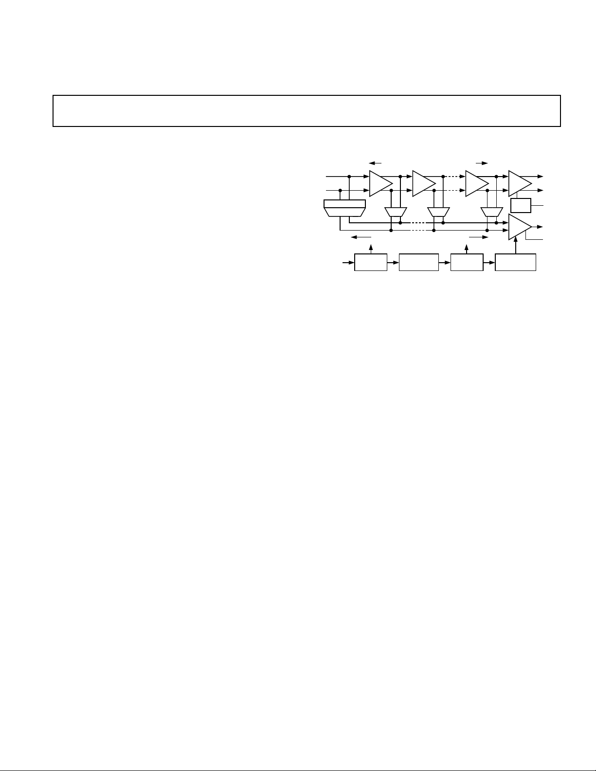
FUNCTIONAL BLOCK DIAGRAM
SIX STAGES TOTAL GAIN 72dB TYP GAIN 18dB
INHI
INLO
LADR ATTEN
ENBL
12dB
TEN DETECTORS SPACED 12dB
GAIN
BIAS
DET DET4 3 DET
BAND-GAP
REFERENCE
12dB
12dB LIM
DET
SLOPE
BIAS
BIAS
CTRL
I–V
INTERCEPT
TEMP COMP
LMHI
LMLO
LMDR
VLOG
FLTR
PRODUCT DESCRIPTION
The AD8306 is a complete IF limiting amplifier, providing both
an accurate logarithmic (decibel) measure of the input signal
(the RSSI function) over a dynamic range of 100 dB, and a
programmable limiter output, useful from 5 MHz to 400 MHz.
It is easy to use, requiring few external components. A single
supply voltage of +2.7 V to +6.5 V at 16 mA is needed, corresponding to a power consumption of under 50 mW at 3 V, plus
the limiter bias current, determined by the application and typi-
cally 2 mA, providing a limiter gain of 90 dB when using 200 Ω
loads. A CMOS-compatible control interface can enable the
AD8306 within about 500 ns and disable it to a standby current
of under 1 µA.
The six cascaded amplifier/limiter cells in the main path have a
small signal gain of 12.04 dB (×4), with a –3 dB bandwidth of
850 MHz, providing a total gain of 72 dB. The programmable
output stage provides a further 18 dB of gain. The input is fully
differential and presents a moderately high impedance (1 kΩ in
parallel with 2.5 pF). The input-referred noise-spectral-density,
when driven from a terminated 50 Ω, source is 1.28 nV/√Hz,
equivalent to a noise figure of 3 dB. The sensitivity of the
AD8306 can be raised by using an input matching network.
Each of the main gain cells includes a full-wave detector. An
additional four detectors, driven by a broadband attenuator, are
used to extend the top end of the dynamic range by over 48 dB.
The overall dynamic range for this combination extends from
–91 dBV (–78 dBm at the 50 Ω level) to a maximum permissible
value of +9 dBV, using a balanced drive of antiphase inputs each of
2 V in amplitude, which would correspond to a sine wave power
of +22 dBm if the differential input were terminated in 50 Ω.
Through laser trimming, the slope of the RSSI output is closely
controlled to 20 mV/dB, while the intercept is set to –108 dBV
(–95 dBm re 50 Ω). These scaling parameters are determined
by a band-gap voltage reference and are substantially independent of temperature and supply. The logarithmic law conform-
ance is typically within ±0.4 dB over the central 80 dB of this
range at any frequency between 10 MHz and 200 MHz, and is
degraded only slightly at 400 MHz.
The RSSI response time is nominally 73 ns (10%–90%). The
averaging time may be increased without limit by the addition of
an external capacitor. The full output of 2.34 V at the maximum
input of +9 dBV can drive any resistive load down to 50 Ω and
this interface remains stable with any value of capacitance on
the output.
The AD8306 is fabricated on an advanced complementary
bipolar process using silicon-on-insulator isolation techniques
and is available in the industrial temperature range of –40°C to
+85°C, in a 16-lead narrow body SO package. The AD8306 is
also available for the full military temperature range of –55°C to
+125°C, in a 16-lead side-brazed ceramic DIP.
REV. A
Information furnished by Analog Devices is believed to be accurate and
reliable. However, no responsibility is assumed by Analog Devices for its
use, nor for any infringements of patents or other rights of third parties
which may result from its use. No license is granted by implication or
otherwise under any patent or patent rights of Analog Devices.
One Technology Way, P.O. Box 9106, Norwood, MA 02062-9106, U.S.A.
Tel: 781/329-4700 World Wide Web Site: http://www.analog.com
Fax: 781/326-8703 © Analog Devices, Inc., 1999
Page 2

AD8306–SPECIFICATIONS
Parameter Conditions Min
INPUT STAGE (Inputs INHI, INLO)
Maximum Input
2
Differential Drive, p-p ±3.5 ±4V
(VS = +5 V, TA = +25ⴗC, f = 10 MHz, unless otherwise noted)
1
Typ Max1Units
+9 dBV
Equivalent Power in 50 Ω Terminated in 52.3 Ω储R
IN
+22 dBm
Noise Floor Terminated 50 Ω Source 1.28 nV/√Hz
Equivalent Power in 50 Ω 400 MHz Bandwidth –78 dBm
Input Resistance From INHI to INLO 800 1000 1200 Ω
Input Capacitance From INHI to INLO 2.5 pF
DC Bias Voltage Either Input 1.725 V
LIMITING AMPLIFIER (Outputs LMHI, LMLO)
Usable Frequency Range 5 400 MHz
At Limiter Output R
LOAD
= R
= 50 Ω, to –10 dB Point 585 MHz
LIM
Phase Variation at 100 MHz Over Input Range –73 dBV to –3 dBV ±2 Degrees
Limiter Output Current Nominally 400 mV/R
Versus Temperature –40°C ≤ T
Input Range
3
≤ +85°C –0.008 %/°C
A
LIM
0110mA
–78 +9 dBV
Maximum Output Voltage At Either LMHI or LMLO, wrt VPS2 1 1.25 V
Rise/Fall Time (10%–90%) R
= 50 Ω, 40 Ω ≤ R
LOAD
≤ 400 Ω 0.6 ns
LIM
LOGARITHMIC AMPLIFIER (Output VLOG)
±3 dB Error Dynamic Range From Noise Floor to Maximum Input 100 dB
Transfer Slope
4
f = 10 MHz 19.5 20 20.5 mV/dB
f = 100 MHz 19.6 mV/dB
Over Temperature –40°C < T
Intercept (Log Offset)
4
f = 10 MHz –109.5 –108 –106.5 dBV
< +85°C 19.3 20 20.7 mV/dB
A
f = 100 MHz –108.4 dBV
Over Temperature –40°C ≤ T
≤ +85°C –111 –108 –105 dBV
A
Temperature Sensitivity –0.009 dB/°C
Linearity Error (Ripple) Input from –80 dBV to +0 dBV ±0.4 dB
Output Voltage Input = –91 dBV, V
Input = +9 dBV, V
Input = –3 dBV, V
Minimum Load Resistance, R
L
= +5 V, +2.7 V 0.34 V
S
= +5 V 2.34 2.75 V
S
= +3 V 2.10 V
S
40 50 Ω
Maximum Sink Current To Ground 0.75 1.0 1.25 mA
Output Resistance 0.3 Ω
Small-Signal Bandwidth 3.5 MHz
Output Settling Time to 2% Large Scale Input, +3 dBV, R
Rise/Fall Time (10%–90%) Large Scale Input, +3 dBV, R
≥␣ 50 Ω, CL ≤␣ 100 pF 120 220 ns
L
≥␣ 50 Ω, CL ≤␣ 100 pF 73 100 ns
L
POWER INTERFACES
Supply Voltage, V
S
2.7 5 6.5 V
Quiescent Current Zero-Signal, LMDR Open 13 16 20 mA
Over Temperature –40°C < T
Disable Current –40°C < T
Additional Bias for Limiter R
LIM
Logic Level to Enable Power HI Condition, –40°C < T
Input Current when HI 3 V at ENBL, –40°C < T
< +85°C 111623mA
A
< +85°C 0.01 4 µA
A
= 400 Ω (See Text) 2.0 2.25 mA
< +85°C 2.7 V
A
< +85°C4060µA
A
V
S
Logic Level to Disable Power LO Condition, –40°C < TA < +85°C –0.5 1 V
TRANSISTOR COUNT # of Transistors 207 207
NOTES
1
Minimum and maximum specified limits on parameters that are guaranteed but not tested are six sigma values.
2
The input level is specified in “dBV” since logarithmic amplifiers respond strictly to voltage, not power. 0 dBV corresponds to a sinusoidal single-frequency input of
1 V rms. A power level of 0 dBm (1 mW) in a 50 Ω termination corresponds to an input of 0.2236 V rms. Hence, in the special case of 50 Ω termination, dBV values
can be converted into dBm by adding a fixed offset of +13 to the dBV rms value.
3
Due to the extremely high Gain Bandwidth Product of the AD8306, the output of either LMHI or LMLO will be unstable for levels below –78 dBV (–65 dBm, re 50 Ω).
4
Standard deviation remains essentially constant over frequency. See Figures 13, 14, 16 and 17.
Specifications subject to change without notice.
–2–
REV. A
Page 3
AD8306
WARNING!
ESD SENSITIVE DEVICE
TOP VIEW
(Not to Scale)
16
15
14
13
12
11
10
9
1
2
3
4
5
6
7
8
COM2
VLOG
AD8306
VPS1
PADL
INHI
INLO
PADL
COM1
ENBL
VPS2
PADL
LMHI
LMLO
PADL
FLTR
LMDR
ABSOLUTE MAXIMUM RATINGS*
Supply Voltage VS . . . . . . . . . . . . . . . . . . . . . . . . . . . . . . 7.5 V
Input Level, Differential (re 50 Ω) . . . . . . . . . . . . . . . +26 dBm
Input Level, Single-Ended (re 50 Ω) . . . . . . . . . . . . . +20 dBm
Internal Power Dissipation . . . . . . . . . . . . . . . . . . . . . 800 mW
. . . . . . . . . . . . . . . . . . . . . . . . . . . . . . . . . . . . . . . 125°C/W
θ
JA
θ
. . . . . . . . . . . . . . . . . . . . . . . . . . . . . . . . . . . . . . . . 25°C/W
JC
Maximum Junction Temperature . . . . . . . . . . . . . . . . +125°C
Operating Temperature Range . . . . . . . . . . . . –40°C to +85°C
Storage Temperature Range
–65°C to +150°C
Lead Temperature Range (Soldering 60 sec)
+300°C
*Stresses above those listed under Absolute Maximum Ratings may cause perma-
nent damage to the device. This is a stress rating only; functional operation of the
device at these or any other conditions above those indicated in the operational
section of this specification is not implied. Exposure to absolute maximum rating
conditions for extended periods may effect device reliability.
ORDERING GUIDE
Temperature Package Package
Model Range Description Options
AD8306AR –40°C to +85°C 16-Lead Narrow Body SO SO-16
AD8306AR-REEL –40°C to +85°C 13" Tape and Reel SO-16
AD8306AR-REEL7 –40°C to +85°C 7" Tape and Reel SO-16
AD8306ACHIPS –40°C to +85°CDie
5962-9864601QEA –55°C to +125°C 16-Lead Side-Brazed Ceramic DIP D-16
AD8306-EVAL Evaluation Board
CAUTION
ESD (electrostatic discharge) sensitive device. Electrostatic charges as high as 4000 V readily
accumulate on the human body and test equipment and can discharge without detection.
Although the AD8306 features proprietary ESD protection circuitry, permanent damage may
occur on devices subjected to high energy electrostatic discharges. Therefore, proper ESD
precautions are recommended to avoid performance degradation or loss of functionality.
PIN FUNCTION DESCRIPTIONS
Pin Name Function
1 COM2 Special Common Pin for RSSI Output.
2 VPS1 Supply Pin for First Five Amplifier Stages
and the Main Biasing System.
3, 6, 11, 14 PADL Four Tie-Downs to the Paddle on
which the IC Is Mounted; Grounded.
4 INHI Signal Input, HI or Plus Polarity.
5 INLO Signal Input, LO or Minus Polarity.
7 COM1 Main Common Connection.
8 ENBL Chip Enable; Active When HI.
9 LMDR Limiter Drive Programming Pin.
10 FLTR RSSI Bandwidth-Reduction Pin.
12 LMLO Limiter Output, LO or Minus Polarity.
13 LMHI Limiter Output, HI or Plus Polarity.
15 VPS2 Supply Pin for Sixth Gain Stage, Limiter
and RSSI Output Stage Load Current.
16 VLOG Logarithmic (RSSI) Output.
REV. A
PIN CONFIGURATION
–3–
Page 4
AD8306
100
–Typical Performance Characteristics
10
0.1
0.01
0.001
SUPPLY CURRENT – mA
0.0001
0.00001
1
0.5
TA = +258C
TA = +858C
0.7 0.9 1.1 1.3 1.5 1.7 1.9 2.1 2.3 2.5
ENABLE VOLTAGE – V
TA = –408C
Figure 1. Supply Current vs. Enable Voltage @
= –40°C, +25°C and +85°C
T
A
14
12
10
8
6
4
SUPPLY CURRENT – mA
LIMITER OUTPUT
2
CURRENT
0
50 100 150 200 250 300 350 400 450
0
ADDITIONAL SUPPLY CURRENT
R
– V
LIM
Figure 2. Additional Supply Current and Limiter Output
Current vs. R
LIM
VLOG
500mV PER
VERTICAL
DIVISION
INPUT LEVEL
SHOWN IS –3dBV
100ns PER HORIZONTAL DIVISION
GROUND REFERENCE
INPUT
1V PER
VERTICAL
DIVISION
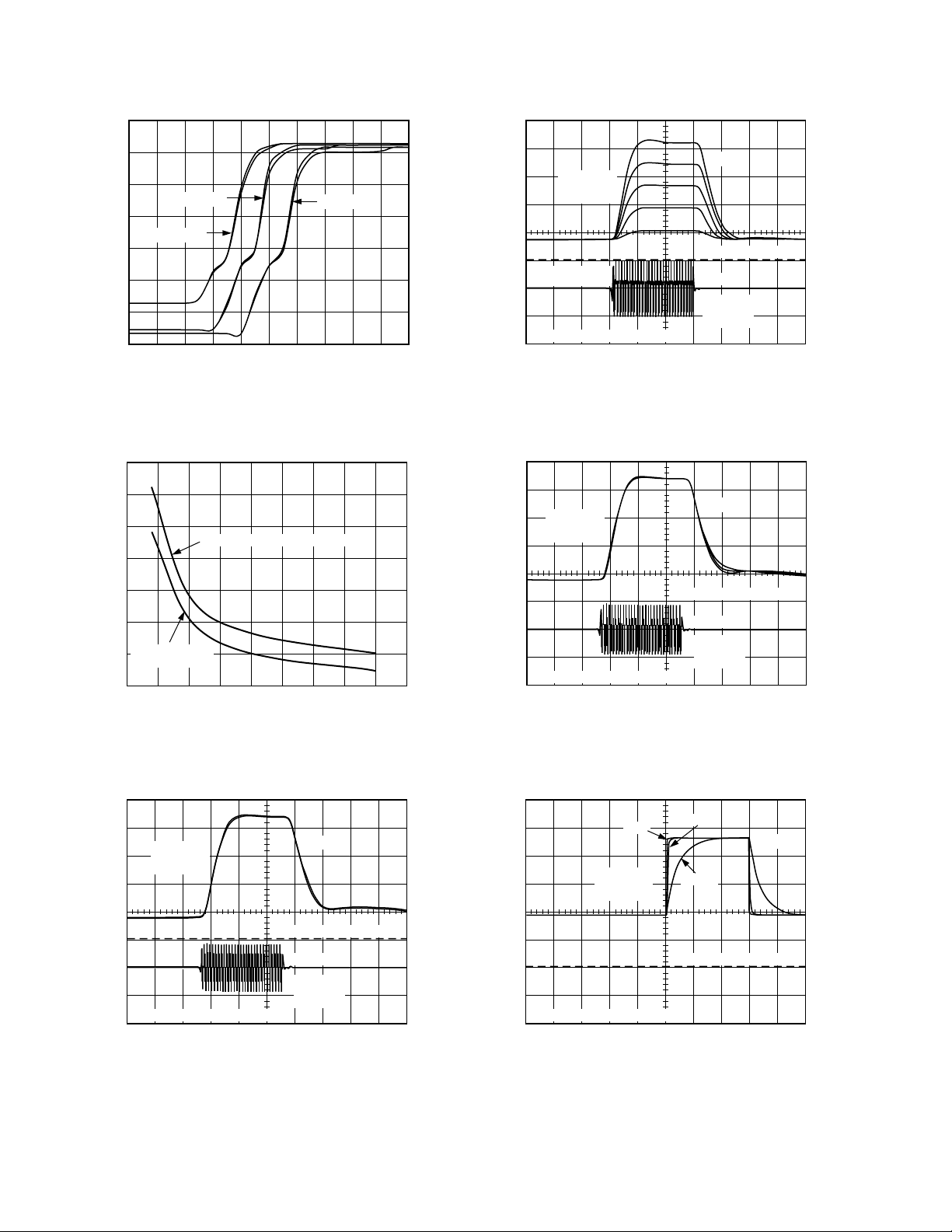
Figure 4. RSSI Pulse Response for Inputs Stepped from
Zero to –83 dBV, –63 dBV, –43 dBV, –23 dBV, –3 dBV
500mV PER
VERTICAL
DIVISION
VLOG
GROUND REFERENCE
INPUT
2V PER
VERTICAL
100ns PER HORIZONTAL DIVISION
DIVISION
Figure 5. Large Signal RSSI Pulse Response with RL = 100
and CL = 33 pF, 100 pF and 330 pF (Overlapping Curves)
Ω
500mV PER
VERTICAL
DIVISION
VLOG
GROUND REFERENCE
INPUT
2V PER
VERTICAL
100ns PER HORIZONTAL DIVISION
DIVISION
Figure 3. Large Signal RSSI Pulse Response with
= 100 pF and RL = 50Ω and 75Ω (Curves Overlap)
C
L
27pF
200mV PER
VERTICAL
DIVISION
270pF
VLOG
3300pF
GROUND REFERENCE
100ms PER HORIZONTAL DIVISION
Figure 6. Small Signal AC Response of RSSI Output with
External Filter Capacitance of 27 pF, 270 pF and 3300 pF
–4–
REV. A
Page 5
AD8306
2.5
2
1.5
1
RSSI OUTPUT – V
0.5
TA = +858C
TA = +258C
0
–120
TA = –408C
–100 –80 –60 –40 –20 0 20
(–87dBm) (+13dBm)
INPUT LEVEL – dBV
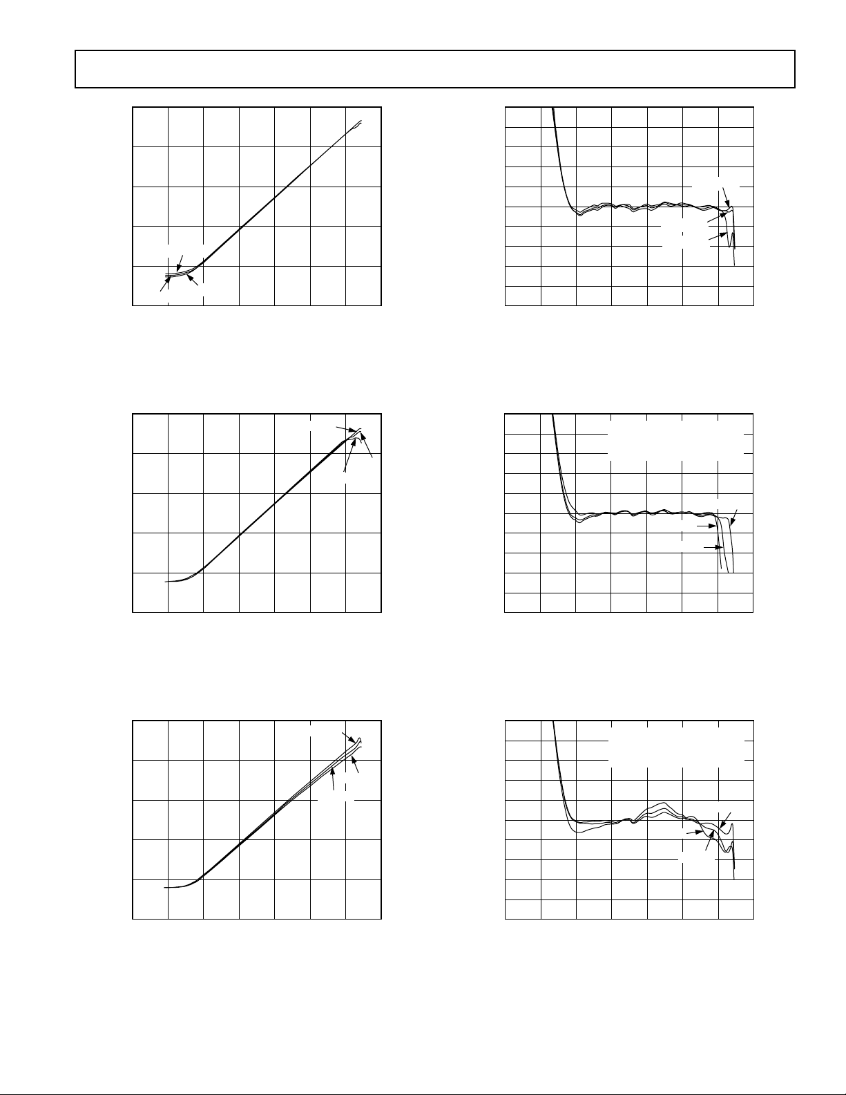
Figure 7. RSSI Output vs. Input Level, 100 MHz Sine Input, at T
= –40°C, +25°C and +85°C, Single-Ended Input
A
2.5
2
1.5
1
RSSI OUTPUT – V
0.5
0
–120
–100 –80 –60 –40 –20 0 20
(–87dBm) (+13dBm)
INPUT LEVEL – dBV
100MHz
50MHz
10MHz
Figure 8. RSSI Output vs. Input Level, at TA = +25°C, for
Frequencies of 10 MHz, 50 MHz and 100 MHz
5
4
3
2
1
0
–1
ERROR – dB
–2
–3
–4
–5
–120
–100 –80 –60 –40 –20 0 20
(–87dBm) (+13dBm)
(–87dBm)
INPUT LEVEL – dBV
TA = +858C
TA = +258C
TA = –408C
Figure 10. Log Linearity of RSSI Output vs. Input Level,
100 MHz Sine Input, at T
5
4
3
2
1
0
–1
ERROR – dB
–2
–3
–4
–5
–120
–100 –80 –60 –40 –20 20
–100
(–87dBm)
= –40°C, +25°C, and +85°C
A
DYNAMIC RANGE 61dB 63dB
10MHz 86 93
50MHz 90 97
100MHz 96 100
10MHz
50MHz
0
INPUT LEVEL – dBV
(+13dBm)
100MHz
Figure 11. Log Linearity of RSSI Output vs. Input Level, at
= +25°C, for Frequencies of 10 MHz, 50 MHz and 100 MHz
T
A
2.5
2
1.5
1
RSSI OUTPUT – V
0.5
0
–120
–100 –80 –60 –40 –20 0 20
(–87dBm) (+13dBm)
INPUT LEVEL – dBV
200MHz
400MHz
300MHz
Figure 9. RSSI Output vs. Input Level, at TA = +25°C, for
Frequencies of 200 MHz, 300 MHz and 400 MHz
REV. A
5
4
3
2
1
0
–1
ERROR – dB
–2
–3
–4
–5
–120
–100 –80 –60 –40 –20 20
–100
(–87dBm)
DYNAMIC RANGE 61dB 63dB
200MHz 96 100
300MHz 90 100
400MHz 85 100
400MHz
300MHz
INPUT LEVEL – dBV
200MHz
0
(+13dBm)
Figure 12. Log Linearity of RSSI Output vs. Input Level,
= +25°C, for Frequencies of 200 MHz, 300 MHz and
at T
A
400 MHz
–5–
Page 6

AD8306
21
20
19
RSSI SLOPE – mV/dB
18
17
0
100 200 300 400
FREQUENCY – MHz
Figure 13. RSSI Slope vs. Frequency Using Termination of
52.3
Ω
0.4
0.375
0.35
–106
–107
–108
–109
–110
RSSI INTERCEPT – dBV
–111
–112
0
100 200 300 400
FREQUENCY – MHz
Figure 16. RSSI Intercept vs. Frequency Using Termination of 52.3
Ω
0.40
0.35
0.30
0.325
0.3
0.275
RSSI SLOPE – STANDARD DEVIATION – %
0.25
0
50 100 150 200
FREQUENCY – MHz
250 300 350 400
Figure 14. RSSI Slope Standard Deviation vs. Frequency
LMLO
LMHI
LIMITER OUTPUTS: 50mV PER VERTICAL DIVISION
INPUT: 1mV PER VERTICAL DIVISION
12.5ns PER HORIZONTAL DIVISION
Figure 15. Limiter Response at LMHI, LMLO with Pulsed
Sine Input of –73 dBV (–60 dBm) at 50 MHz; R
= 200
R
LIM
Ω
LOAD
= 50 Ω,
0.25
0.20
0.15
RSSI INTERCEPT – STANDARD DEVIATION – dB
0.10
0
50 100 150 200
FREQUENCY – MHz
250 300 350 400
Figure 17. RSSI Intercept Standard Deviation vs. Frequency
10
8
6
4
2
TA = +858C
0
–2
TA = +258C
–4
–6
NORMALIZED PHASE SHIFT – Degrees
–8
–10
–73
–63 –53 –43 –33 –23 –13 –3
(–50dBm) (0dBm)
TA = –408C
INPUT LEVEL – dBV
Figure 18. Normalized Limiter Phase Response vs. Input
Level. Frequency = 100 MHz; T
= –40°C, +25°C and +85°C
A
–6–
REV. A
Page 7

AD8306
PRODUCT OVERVIEW
The AD8306 is built on an advanced dielectrically-isolated
complementary bipolar process using thin-film resistor technology for accurate scaling. It follows well-developed foundations
proven over a period of some fifteen years, with constant refinement. The backbone of the AD8306 (Figure 19) comprises a
chain of six main amplifier/limiter stages, each having a gain of
12.04 dB (×4) and small-signal –3 dB bandwidth of 850 MHz.
The input interface at INHI and INLO (Pins 4 and 5) is fully
differential. Thus it may be driven from either single-sided or
balanced inputs, the latter being required at the very top end of
the dynamic range, where the total differential drive may be as
large as 4 V in amplitude.
The first six stages, also used in developing the logarithmic
RSSI output, are followed by a versatile programmable-output,
and thus programmable-gain, final limiter section. Its opencollector outputs are also fully differential, at LMHI and LMLO
(Pins 12 and 13). This output stage provides a gain of 18 dB
when using equal valued load and bias setting resistors and the
pin-to-pin output is used. The overall voltage gain is thus 90 dB.
When using R
LIM
= R
= 200 Ω, the additional current
LOAD
consumption in the limiter is approximately 2.8 mA, of which
2 mA goes to the load. The ratio depends on R
(for example,
LIM
when 20 Ω, the efficiency is 90%), and the voltage at the pin
LMDR is rather more than 400 mV, but the total load current
is accurately (400 mV)/R
LIM
.
The rise and fall times of the hard-limited (essentially squarewave) voltage at the outputs are typically 0.6 ns, when driven by
a sine wave input having an amplitude of 316 µV or greater, and
R
= 50 Ω. The change in time-delay (“phase skew”) over
LOAD
the input range –73 dBV (316 µV in amplitude, or –60 dBm in
50 Ω) to –3 dBV (1 V or +10 dBm) is ±56 ps (±2° at 100 MHz).
SIX STAGES TOTAL GAIN 72dB TYP GAIN 18dB
INHI
INLO
LADR ATTEN
ENBL
12dB
TEN DETECTORS SPACED 12dB
GAIN
BIAS
DET DET4 3 DET
BAND-GAP
REFERENCE
12dB
12dB LIM
DET
SLOPE
BIAS
BIAS
CTRL
I–V
INTERCEPT
TEMP COMP
LMHI
LMLO
LMDR
VLOG
FLTR
Figure 19. Main Features of the AD8306
The six main cells and their associated full-wave detectors,
having a transconductance (g
) form, handle the lower part of
m
the dynamic range. Biasing for these cells is provided by two
references, one of which determines their gain, the other being a
band-gap cell which determines the logarithmic slope, and stabilizes it against supply and temperature variations. A special
dc-offset-sensing cell (not shown in Figure 19) is placed at the
end of this main section, and used to null any residual offset at
the input, ensuring accurate response down to the noise floor.
The first amplifier stage provides a short-circuited voltage-noise
spectral-density of 1.07 nV/√Hz.
The last detector stage includes a modification to temperaturestabilize the log-intercept, which is accurately positioned so as
to make optimal use of the full output voltage range. Four further “top end” detectors are placed at 12.04 dB taps along a
passive attenuator, to handle the upper part of the range. The
differential current-mode outputs of all ten detectors stages are
summed with equal weightings and converted to a single-sided
voltage by the output stage, generating the logarithmic (or RSSI)
output at VLOG (Pin 16), nominally scaled 20 mV/dB (that is,
400 mV per decade). The junction between the lower and upper
regions is seamless, and the logarithmic law-conformance is
typically well within ±0.4 dB over the 80 dB range from –80 dBV
to 0 dBV (–67 dBm to +13 dBm).
The full-scale rise time of the RSSI output stage, which operates
as a two-pole low-pass filter with a corner frequency of 3.5 MHz,
is about 200 ns. A capacitor connected between FLTR (Pin 10)
and VLOG can be used to lower the corner frequency (see below). The output has a minimum level of about 0.34 V (corresponding to a noise power of –78 dBm, or 17 dB above the
nominal intercept of –95 dBm). This rather high baseline level
ensures that the pulse response remains unimpaired at very low
inputs.
The maximum RSSI output depends on the supply voltage and
the load. An output of 2.34 V, that is, 20 mV/dB × (9 + 108) dB, is
guaranteed when using a supply voltage of 4.5 V or greater and
a load resistance of 50 Ω or higher, for a differential input of
9 dBV (a 4 V sine amplitude, using balanced drives). When
using a 3 V supply, the maximum differential input may still be
as high as –3 dBV (1 V sine amplitude), and the corresponding
RSSI output of 2.1 V, that is, 20 mV/dB × (–3 + 108) dB is also
guaranteed.
A fully-programmable output interface is provided for the hardlimited signal, permitting the user to establish the optimal output
current from its differential current-mode output. Its magnitude
is determined by the resistor R
placed between LMDR (Pin
LIM
9) and ground, across which a nominal bias voltage of ~400 mV
appears. Using R
= 200 Ω, this dc bias current, which is
LIM
commutated alternately to the output pins, LMHI and LMLO,
by the signal, is 2 mA. (The total supply current is somewhat
higher).
These currents may readily be converted to voltage form by the
inclusion of load resistors, which will typically range from a few
tens of ohms at 400 MHz to as high as 2 kΩ in lower frequency
applications. Alternatively, a resonant load may be used to extract
the fundamental signal and modulation sidebands, minimizing
the out-of-band noise. A transformer or impedance matching
network may also be used at this output. The peak voltage swing
down from the supply voltage may be 1.2 V, before the output
transistors go into saturation. (The Applications section provides
further information on the use of this interface).
The supply current for all sections except the limiter output
stage, and with no load attached to the RSSI output, is nominally 16 mA at T
= 27°C, substantially independent of supply
A
voltage. It varies in direct proportion to the absolute temperature (PTAT). The RSSI load current is simply the voltage at
VLOG divided by the load resistance (e.g., 2.4 mA max in a
1 kΩ load). The limiter supply current is 1.1 times that flowing
. The AD8306 may be enabled/disabled by a CMOS-
in R
LIM
compatible level at ENBL (Pin 8).
In the following simplified interface diagrams, the components
denoted with an uppercase “R” are thin-film resistors having a
very low temperature-coefficient of resistance and high linearity
under large-signal conditions. Their absolute value is typically
within ±20%. Capacitors denoted using an uppercase “C” have
a typical tolerance of ±15% and essentially zero temperature or
REV. A
–7–
Page 8

AD8306
voltage sensitivity. Most interfaces have additional small junction capacitances associated with them, due to active devices or
ESD protection; these may be neither accurate nor stable.
Component numbering in each of these interface diagrams is
local.
Enable Interface
The chip-enable interface is shown in Figure 20. The current in
R1 controls the turn-on and turn-off states of the band-gap
reference and the bias generator, and is a maximum of 100 µA
when Pin 8 is taken to 5 V. Left unconnected, or at any voltage
below 1 V, the AD8306 will be disabled, when it consumes a
sleep current of much less than 1 µA (leakage currents only); when
tied to the supply, or any voltage above 2 V, it will be fully enabled.
The internal bias circuitry requires approximately 300 ns for
either OFF or ON, while a delay of some 6 µs is required for the
supply current to fall below 10 µA.
ENBL
COMM
60kV
R1
1.3kV
TO BIAS
ENABLE
50kV 4kV
Figure 20. Enable Interface
Input Interface
Figure 21 shows the essentials of the signal input interface. The
parasitic capacitances to ground are labeled C
input capacitance, C
, mainly due to the diffusion capacitance
D
; the differential
P
of Q1 and Q2. In most applications both input pins are accoupled. The switch S closes when Enable is asserted. When
disabled, the inputs float, bias current I
is shut off, and the
E
coupling capacitors remain charged. If the log amp is disabled
for long periods, small leakage currents will discharge these
capacitors. If they are poorly matched, charging currents at
power-up can generate a transient input voltage which may
block the lower reaches of the dynamic range until it has become much less than the signal.
handled using a supply of 4.5 V or greater. When using a fullybalanced drive, the +3 dBV level may be achieved for the supplies down to 2.7 V and +9 dBV using >4.5 V. For frequencies
in the range 10 MHz to 200 MHz these high drive levels are
easily achieved using a matching network. Using such a network, having an inductor at the input, the input transient is
eliminated.
Limiter Output Interface
The simplified limiter output stage is shown in Figure 22. The
bias for this stage is provided by a temperature-stable reference
voltage of nominally 400 mV which is forced across the external resistor R
connected from Pin 9 (LMDR, or limiter
LIM
drive) by a special op amp buffer stage. The biasing scheme
also introduces a slight “lift” to this voltage to compensate for
the finite current gain of the current source Q3 and the output
transistors Q1 and Q2. A maximum current of 10 mA is permissible (R
= 40 Ω). In special applications, it may be desir-
LIM
able to modulate the bias current; an example of this is provided
in the Applications section. Note that while the bias currents are
temperature stable, the ac gain of this stage will vary with tem-
perature, by –6 dB over a 120°C range.
A pair of supply and temperature stable complementary currents is generated at the differential output LMHI and LMLO
(Pins 12 and 13), having a square wave form with rise and fall
times of typically 0.6 ns, when load resistors of 50 Ω are used.
The voltage at these output pins may swing to 1.2 V below the
supply voltage applied to VPS2 (Pin 15).
Because of the very high gain bandwidth product of this amplifier considerable care must be exercised in using the limiter
outputs. The minimum necessary bias current and voltage
swings should be used. These outputs are best utilized in a
fully-differential mode. A flux-coupled transformer, a balun, or
an output matching network can be selected to transform these
voltages to a single-sided form. Equal load resistors are recommended, even when only one output pin is used, and these
should always be returned to the same well decoupled node on
the PC board. When the AD8306 is used only to generate an
RSSI output, the limiter should be completely disabled by
omitting R
and strapping LMHI and LMLO to VPS2.
LIM
VPS2 LMHI LMLO
C
C
SIGNAL
INPUT
C
C
COMM
VPS1
INLO
INHI
1.78V
RIN = 1kV
S
3.65kV 3.65kV
1.725V
C
P
2.5pF
DETECTORS)
1.725V
IB = 15mA
C
D
2.6kV
(TOP-END
RIN = 3kV
C
P
130V
Q1
20e
TO STAGES
1 THRU 5
67V67V
TO 2ND
STAGE
Q2
20e
GAIN BIAS
1.26V
3.4mA
PTAT
Figure 21. Signal Input Interface
In most applications, the input signal will be single-sided, and
may be applied to either Pin 4 or 5, with the remaining pin accoupled to ground. Under these conditions, the largest input
signal that can be handled is –3 dBV (sine amplitude of 1 V)
when operating from a 3 V supply; a +3 dBV input may be
–8–
1.3kV1.3kV
Q1
FROM FINAL
LIMITER STAGE
2.6kV
4e
Q2
4e
Q3
1.3kV1.3kV
LMDR
R
LIM
OA
400mV
ZERO-TC
COM1
Figure 22. Limiter Output Interface
RSSI Output Interface
The outputs from the ten detectors are differential currents,
having an average value that is dependent on the signal input
level, plus a fluctuation at twice the input frequency. The currents are summed at the internal nodes LGP and LGN shown
in Figure 23. A further current I
is added to LGP, to position
T
REV. A
Page 9

AD8306
the intercept to –108 dBV, by raising the RSSI output voltage for
zero input, and to provide temperature compensation, resulting
in a stable intercept. For zero signal conditions, all the detector
output currents are equal. For a finite input, of either polarity,
their difference is converted by the output interface to a singlesided voltage nominally scaled 20 mV/dB (400 mV per decade), at
the output VLOG (Pin 16). This scaling is controlled by a separate feedback stage, having a tightly controlled transconductance. A small uncertainty in the log slope and intercept
remains (see Specifications); the intercept may be adjusted (see
Applications).
VPS2
FLTR
C
VLOG
20mV/dB
COMM
F
SUMMED
DETECTOR
OUTPUTS
LGP
LGN
I
T
VLOG
TRANSCONDUCTANCE
DETERMINES SLOPE
1.3kV1.3kV
250ms
CURRENT
MIRROR
125mA
ON DEMAND
3.3kV3.3kV
I
SOURCE
>50mA
C1
3.5pF
I
SINK
FIXED
1mA
Figure 23. Simplified RSSI Output Interface
The RSSI output bandwidth, fLP, is nominally 3.5 MHz. This is
controlled by the compensation capacitor C1, which may be
increased by adding an external capacitor, C
(Pin 10) and VLOG (Pin 16). An external 33 pF will reduce f
, between FLTR
F
LP
to 350 kHz, while 360 pF will set it to 35 kHz, in each case with
an essentially one-pole response. In general, the relationships
in MHz) are:
(for f
LP
C
=
F
×
12 7 10
.
f
LP
10 6
–
35
–. ;
pF f
12 7 10
=
LP
CpF
F
.
+
×
35
.
−
(1)
Using a load resistance of 50 Ω or greater, and at any tempera-
ture, the peak output voltage may be at least 2.4 V when using a
supply of 4.5 V, and at least 2.1 V for a 3 V supply, which is
consistent with the maximum permissible input levels. The incre-
mental output resistance is approximately 0.3 Ω at low frequen-
cies, rising to 1 Ω at 150 kHz and 18 Ω at very high frequencies.
The output is unconditionally stable with load capacitance, but
it should be noted that while the peak sourcing current is
over 100 mA, and able to rapidly charge even large capacitances,
the internally provided sinking current is only 1 mA. Thus, the
fall time from the 2 V level will be as long as 2 µs for a 1 nF
load. This may be reduced by adding a grounded load resistance.
USING THE AD8306
The AD8306 exhibits very high gain from 1 MHz to over 1 GHz,
at which frequency the gain of the main path is still over 65 dB.
Consequently, it is susceptible to all signals, within this very
broad frequency range, that find their way to the input terminals. It is important to remember that these are quite indistinguishable from the “wanted” signal, and will have the effect of
raising the apparent noise floor (that is, lowering the useful
dynamic range). Therefore, while the signal of interest may be
an IF of, say, 200 MHz, any of the following could easily be
larger than this signal at the lower extremities of its dynamic
range: a 60 Hz hum, picked up due to poor grounding techniques; spurious coupling from digital logic on the same PC
board; a strong EMI source; etc.
Very careful shielding is essential to guard against such unwanted signals, and also to minimize the likelihood of instability
due to HF feedback from the limiter outputs to the input. With
this in mind, the minimum possible limiter gain should be used.
Where only the logarithmic amplifier (RSSI) function is required, the limiter should be disabled by omitting R
LIM
and
tying the outputs LMHI and LMLO directly to VPS2. A good
ground plane should be used to provide a low impedance connection to the common pins, for the decoupling capacitor(s)
used at VPS1 and VPS2, and at the output ground. Note that
COM2 is a special ground pin serving just the RSSI output.
The four pins labeled PADL tie down directly to the metallic
lead frame, and are thus connected to the back of the chip. The
process on which the AD8306 is fabricated uses a bonded-wafer
technique to provide a silicon-on-insulator isolation, and there is
no junction or other dc path from the back side to the circuitry
on the surface. These paddle pins must be connected directly to
the ground plane using the shortest possible lead lengths to
minimize inductance.
The voltages at the two supply pins should not be allowed to
differ greatly; up to 500 mV is permissible. It is desirable to
allow VPS1 to be slightly more negative than VPS2. When the
primary supply is greater than 2.7 V, the decoupling resistors R1
and R2 (Figure 24) may be increased to improve the isolation
and lower the dissipation in the IC. However, since VPS2 supports the RSSI load current, which may be large, the value of
R2 should take this into account.
Basic Connections for Log (RSSI) Output
Figure 24 shows the connections required for most applications.
The AD8306 is enabled by connecting ENBL to VPS1. The
device is put into the sleep mode by grounding this pin. The
inputs are ac-coupled by C1 and C2, which normally should
have the same value (C
). The input is, in this case, terminated
C
with a 52.3 Ω resistor that combines with the AD8306’s input
resistance of 1000 Ω to give a broadband input impedance of
50 Ω. Alternatively an input matching network can be used (see
Input Matching section).
0.1mF
VS (2.7V TO 6.5V)
RSSI
C
F
(OPTIONAL
SEE TEXT)
SIGNAL
INPUTS
C1
0.01mF
C2
0.01mF
R1
10V
0.1mF
ENABLE
R
T
52.3V
1
2
3
4
5
6
7
8
COM2
VPS1
PADL
INHI
INLO
PADL
COM1
ENBL
AD8306
VLOG
VPS2
PADL
LMHI
LMLO
PADL
FLTR
LMDR
R2
10V
16
15
14
13
12
11
10
9
Figure 24. Basic Connections for RSSI (Log) Output
The 0.01 µF coupling capacitors and the resulting 50 Ω input
impedance give a high-pass corner frequency of around 600 kHz.
(1/(2 π RC)), where C = (C1)/2. In high frequency applications,
this corner frequency should be placed as high as possible, to
minimize the coupling of unwanted low frequency signals. In
REV. A
–9–
Page 10

AD8306
low frequency applications, a simple RC network forming a lowpass filter should be added at the input for the same reason.
If the limiter output is not required, Pin 9 (LMDR) should be
left open and Pins 12 and 13 (LMHI, LMLO) should be tied to
VPS2 as shown in Figure 24.
Figure 25 shows the output versus the input level in dBV, for
sine inputs at 10 MHz, 50 MHz and 100 MHz (add 13 to the
dBV number to get dBm Re 50 Ω. Figure 26 shows the typi-
cal logarithmic linearity (log conformance) under the same
conditions.
2.5
2
1.5
1
RSSI OUTPUT – V
0.5
0
–120
–100 –80 –60 –40 –20 0 20
INPUT LEVEL – dBV
100MHz
50MHz
10MHz
Figure 25. RSSI Output vs. Input Level at TA = +25°C for
Frequencies of 10 MHz, 50 MHz and 100 MHz
5
4
3
2
1
0
–1
ERROR – dB
–2
–3
–4
–5
–120
–100 –80 –60 –40 –20 20
–100
DYNAMIC RANGE 61dB 63dB
10MHz 86 93
50MHz 90 97
100MHz 96 100
10MHz
50MHz
INPUT LEVEL – dBV
100MHz
0
Figure 26. Log Linearity vs. Input Level at TA = +25°C, for
Frequencies of 10 MHz, 50 MHz and 100 MHz
Transfer Function in Terms of Slope and Intercept
The transfer function of the AD8306 is characterized in terms
of its Slope and Intercept. The logarithmic slope is defined as
the change in the RSSI output voltage for a 1 dB change at the
input. For the AD8306 the slope is calibrated to be 20 mV/dB.
The intercept is the point at which the extrapolated linear response would intersect the horizontal axis. For the AD8306 the
intercept is calibrated to be –108 dBV (–95 dBm). Using the
slope and intercept, the output voltage can be calculated for any
input level within the specified input range using the equation:
V
OUT
= V
SLOPE
× (P
– PO) (2)
IN
where V
V
SLOPE
is the demodulated and filtered RSSI output,
OUT
is the logarithmic slope, expressed in V/dB, PIN is the
input signal, expressed in decibels relative to some reference
level (either dBm or dBV in this case) and P
is the logarithmic
O
intercept, expressed in decibels relative to the same reference
level.
For example, for an input level of –33 dBV (–20 dBm), the
output voltage will be
V
= 0.02 V/dB × (–33 dBV – (–108 dBV)) = 1.5 V (3)
OUT
The most widely used convention in RF systems is to specify
power in dBm, that is, decibels above 1 mW in 50 Ω. Specifica-
tion of log amp input level in terms of power is strictly a concession to popular convention; they do not respond to power (tacitly
“power absorbed at the input”), but to the input voltage. The
use of dBV, defined as decibels with respect to a 1 V rms sine wave,
is more precise, although this is still not unambiguous because
waveform is also involved in the response of a log amp, which,
for a complex input (such as a CDMA signal) will not follow the
rms value exactly. Since most users specify RF signals in terms
of power—more specifically, in dBm/50 Ω—we use both dBV
and dBm in specifying the performance of the AD8306, showing
equivalent dBm levels for the special case of a 50 Ω environment.
Values in dBV are converted to dBm re 50 Ω by adding 13.
Output Response Time and C
F
The RSSI output has a low-pass corner frequency of 3.5 MHz,
which results in a 10% to 90% rise time of 73 ns. For low frequency applications, the corner frequency can be reduced by
adding an external capacitor, C
, between FLTR (Pin 10) and
F
VLOG (Pin 16) as shown in Figure 24. For example, an external 33 pF will reduce the corner frequency to 350 kHz, while
360 pF will set it to 35 kHz, in each case with an essentially
one-pole response.
Using the Limiter
Figure 27 shows the basic connections for operating the limiter
and the log output concurrently. The limiter output is a pair of
differential currents of magnitude, I
, from high impedance
OUT
(open-collector) sources. These are converted to equal-amplitude
voltages by supply-referenced load resistors, R
output current is set by R
, the resistor connected between
LIM
. The limiter
LOAD
Pin 9 (LMDR) and ground. The limiter output current is set
according the equation:
I
= –400 mV/R
OUT
LIM
(5)
and has an absolute accuracy of ±5%.
The supply referenced voltage on each of the limiter pins will
thus be given by:
V
= V
LIM
–400 mV × R
S
LOAD/RLIM
(6)
–10–
REV. A
Page 11
AD8306
0.1mF
R
LOAD
R
L
(SEE TEXT)
VS (2.7V TO 6.5V)
RSSI
0.01mF
LIMITER
OUTPUT
0.01mF
SIGNAL
INPUTS
C1
0.01mF
C2
0.01mF
10V
0.1mF
ENABLE
R1
R
52.3V
T
1
COM2
2
VPS1
3
PADL
AD8306
4
INHI
5
INLO
6
PADL
7
COM1
ENBL
8
NC = NO CONNECT
VLOG
VPS2
PADL
LMHI
LMLO
PADL
FLTR
LMDR
R2
10V
16
15
14
13
12
11
10
NC
R
LIM
9
Figure 27. Basic Connections for Operating the Limiter
Depending on the application, the resulting voltage may be used
in a fully balanced or unbalanced manner. It is good practice to
retain both load resistors, even when only one output pin is
used. These should always be returned to the same well decoupled node on the PC board (see layout of evaluation board).
The unbalanced, or single-sided mode, is more inclined to result
in instabilities caused by the very high gain of the signal path.
The limiter current may be set as high as 10 mA (which requires
to be 40 Ω) and can be optionally increased somewhat
R
LIM
beyond this level. It is generally inadvisable, however, to use a
high bias current, since the gain of this wide bandwidth signal
path is proportional to the bias current, and the risk of instability is elevated as R
However, as the size of R
limiter output decreases from 585 MHz for R
50 Ω to 50 MHz for R
210 MHz for R
= 200 Ω). As a result, the minimum necessary limiter
R
LIM
is reduced (recommended value is 400 Ω).
LIM
is increased, the bandwidth of the
LOAD
LOAD
LOAD
LOAD
= R
= R
= 400 Ω (bandwidth =
LIM
= 100 Ω and 100 MHz for R
LIM
= R
LIM
LOAD
=
=
output level should be chosen while maintaining the required
limiter bandwidth. For R
LIM
= R
= 50 Ω, the limiter output
LOAD
is specified for input levels between –78 dBV (–65 dBm) and
+9 dBV (+22 dBm). The output of the limiter may be unstable
for levels below –78 dBV (–65 dBm). However, keeping R
LIM
above 100 Ω will make instabilities on the output less likely for
input levels below –78 dBV.
A transformer or a balun (e.g., MACOM part number ETC1-1-13)
can be used to convert the differential limiter output voltages to
a single-ended signal.
Input Matching
Where either a higher sensitivity or a better high frequency
match is required, an input matching network is valuable. Using
a flux-coupled transformer to achieve the impedance transformation also eliminates the need for coupling capacitors, lowers
any dc offset voltages generated directly at the input, and usefully balances the drives to INHI and INLO, permitting full
utilization of the unusually large input voltage capacity of the
AD8306.
The choice of turns ratio will depend somewhat on the frequency. At frequencies below 30 MHz, the reactance of the
input capacitance is much higher than the real part of the input
impedance. In this frequency range, a turns ratio of 2:9 will
lower the effective input impedance to 50 Ω while raising the
input voltage by 13 dB. However, this does not lower the effect
of the short circuit noise voltage by the same factor, since there
will be a contribution from the input noise current. Thus, the
total noise will be reduced by a smaller factor. The intercept at
the primary input will be lowered to –121 dBV (–108 dBm).
Impedance matching and drive balancing using a flux-coupled
transformer is useful whenever broadband coupling is required.
However, this may not always be convenient. At high frequencies, it will often be preferable to use a narrow-band matching
network, as shown in Figure 28, which has several advantages.
First, the same voltage gain can be achieved, providing increased
sensitivity, but now a measure of selectively is simultaneously
introduced. Second, the component count is low: two capacitors
and an inexpensive chip inductor are needed. Third, the network also serves as a balun. Analysis of this network shows that
the amplitude of the voltages at INHI and INLO are quite simi-
lar when the impedance ratio is fairly high (i.e., 50 Ω to 1000 Ω).
V
10V
COM2
0.1mF
C1 = C
M
Z
IN
C2 = C
L
M
M
1
VPS1
2
3
PADL
AD8306
4
INHI
INLO
5
PADL
6
COM1
7
ENBL
8
NC = NO CONNECT
VLOG
VPS2
PADL
LMHI
LMLO
PADL
FLTR
LMDR
10V
16
0.1mF
15
14
13
12
11
10
NC
R
LIM
9
S
RSSI
LIMITER
OUTPUT
Figure 28. High Frequency Input Matching Network
Figure 29 shows the response for a center frequency of 100 MHz.
The response is down by 50 dB at one-tenth the center frequency,
falling by 40 dB per decade below this. The very high frequency
attenuation is relatively small, however, since in the limiting
case it is determined simply by the ratio of the AD8306’s input
capacitance to the coupling capacitors. Table I provides solutions for a variety of center frequencies f
impedances Z
of nominally 50 Ω and 100 Ω. Exact values are
IN
and matching from
C
shown, and some judgment is needed in utilizing the nearest
standard values.
14
13
12
11
10
9
8
7
6
DECIBELS
5
4
3
2
1
0
–1
60
70 80 90 100 110 120 130
GAIN
INPUT AT
TERMINATION
FREQUENCY – MHz
140 150
Figure 29. Response of 100 MHz Matching Network
REV. A
–11–
Page 12

AD8306
Table I.
Match to 50 ⍀ Match to 100 ⍀
(Gain = 13 dB) (Gain = 10 dB)
f
C
C
M
L
M
C
M
L
M
MHz pF nH pF nH
10 140 3500 100.7 4790
10.7 133 3200 94.1 4460
15 95.0 2250 67.1 3120
20 71.0 1660 50.3 2290
21.4 66.5 1550 47.0 2120
25 57.0 1310 40.3 1790
30 47.5 1070 33.5 1460
35 40.7 904 28.8 1220
40 35.6 779 25.2 1047
45 31.6 682 22.4 912
50 28.5 604 20.1 804
60 23.7 489 16.8 644
80 17.8 346 12.6 448
100 14.2 262 10.1 335
120 11.9 208 8.4 261
150 9.5 155 6.7 191
200 7.1 104 5.03 125
250 5.7 75.3 4.03 89.1
300 4.75 57.4 3.36 66.8
350 4.07 45.3 2.87 52.1
400 3.57 36.7 2.52 41.8
450 3.16 30.4 2.24 34.3
500 2.85 25.6 2.01 28.6
General Matching Procedure
For other center frequencies and source impedances, the following
method can be used to calculate the basic matching parameters.
Step 1: Tune Out C
IN
At a center frequency fC, the shunt impedance of the input
capacitance C
temporary inductor L
L
= 1/{(2 π fC)2CIN} = 1010/f
IN
when C
IN
can be made to disappear by resonating with a
IN
, whose value is given by
IN
2
C
= 2.5 pF. For example, at fC = 100 MHz, L
= 1 µH.
IN
(7)
Step 2: Calculate CO and L
O
Now having a purely resistive input impedance, we can calculate
the nominal coupling elements C
C
=
O
1
2
π
fRR
CINM
()
For the AD8306, R
needed, at f
= 100 MHz, CO must be 7.12 pF and LO must be
C
;
is 1 kΩ. Thus, if a match to 50 Ω is
IN
and LO, using
O
RR
IN M
()
L
=
O
2
π
f
C
(8)
356 nH.
Step 3: Split CO Into Two Parts
Since we wish to provide the fully-balanced form of network
shown in Figure 28, two capacitors C1 = C2
twice C
, shown as CM in the figure, can be used. This requires
O
each of nominally
a value of 14.24 pF in this example. Under these conditions, the
voltage amplitudes at INHI and INLO will be similar. A somewhat better balance in the two drives may be achieved when C1
is made slightly larger than C2, which also allows a wider range
of choices in selecting from standard values. For example, capacitors of C1 = 15 pF and C2 = 13 pF may be used (making
= 6.96 pF).
C
O
Step 4: Calculate L
M
The matching inductor required to provide both LIN and LO is
just the parallel combination of these:
L
= LINLO/(LIN + LO) (9)
M
With L
= 1 µH and L
IN
= 356 nH, the value of LM to complete
O
this example of a match of 50 Ω at 100 MHz is 262.5 nH. The
nearest standard value of 270 nH may be used with only a slight
loss of matching accuracy. The voltage gain at resonance depends only on the ratio of impedances, as is given by
GAIN
R
=
20 10log log
IN
=
R
S
R
IN
R
S
(10)
Altering the Logarithmic Slope
Simple schemes can be used to increase and decrease the logarithmic slope as shown in Figure 30. For the AD8306, only
power, ground and logarithmic output connections are shown;
refer to Figure 24 for complete circuitry. In Figure 30(a), the op
amp’s gain of +2 increases the slope to 40 mV/dB. In Figure
30(b), the AD8031 buffers a resistive divider to give a slope of
0.1mF
10V 10V
VPS1 VPS2
AD8306
PADL, COM1, COM2
VLOG
0.1mF
(a)
AD8031
5kV
+5V
10V
0.1mF
40mV/dB
5kV
0.1mF
Figure 30. Altering the Logarithmic Slope
–12–
10V 10V
VPS1 VPS2
VLOG
AD8306
PADL, COM1, COM2
0.1mF
5kV
5kV
(b)
AD8031
+5V
10V
0.1mF
10mV/dB
REV. A
Page 13

AD8306
10 mV/dB The AD8031 rail-to-rail op amp, used in both examples, can swing from 50 mV to 4.95 mV on a single +5 V
supply. If high output current is required (> 10 mA), the AD8051,
which also has rail-to-rail capability but can deliver up to 45 mA
of output current, can be used.
APPLICATIONS
The AD8306 is a versatile and easily applied log-limiting amplifier. Being complete, it can be used with very few external components, and most applications can be accommodated using the
simple connections shown in the preceding section. A few examples of more specialized applications are provided here.
High Output Limiter Loading
The AD8306 can generate a fairly large output power at its
differential limiter output interface. This may be coupled into a
50 Ω grounded load using the narrow-band coupling network
following similar lines to those provided for input matching.
Alternatively, a flux-linked transformer, having a center-tapped
primary, may be used. Even higher output powers can be obtained using emitter-followers. In Figure 31, the supply voltage
to the AD8306 is dropped from 5 V to about 4.2 V, by the
diode. This increases the available swing at each output to about
2 V. Taking both outputs differentially, a square wave output of
4 V p-p can be generated.
10V
0.1mF
APPROX. 4.2V
COM2
1
VPS1
2
3
PADL
4
INHI
INLO
5
PADL
6
COM1
7
ENBL
8
AD8306
VLOG
VPS2
PADL
LMHI
LMLO
PADL
FLTR
LMDR
IN914
R
0.1mF
LIM
LOAD
RSSI
10V
16
15
14
13
12
11
10
R
9
+5V
R
LOAD
SET RL = 5*R
3V TO 5V
5V TO 3V
DIFFERENTIAL
OUTPUT = 4V pk-pk
LIM
Figure 31. Increasing Limiter Output Voltage
When operating at high output power levels and high frequencies, very careful attention must be paid to the issue of stability.
Oscillation is likely to be observed when the input signal level is
low, due to the extremely high gain-bandwidth product of the
AD8306 under such conditions. These oscillations will be less
evident when signal-balancing networks are used, operating at
frequencies below 200 MHz, and they will generally be fully
quenched by the signal at input levels of a few dB above the
noise floor.
Modulated Limiter Output
The limiter output stage of the AD8306 also provides an analog
multiplication capability: the amplitude of the output square
wave can be controlled by the current withdrawn from LMDR
(Pin 9). An analog control input of 0 V to +1 V is used to generate an exactly-proportional current of 0 mA to 10 mA in the npn
transistor, whose collector is held at a fixed voltage of ∼400 mV
by the internal bias in the AD8306. When the input signal is
above the limiting threshold, the output will then be a squarewave whose amplitude is proportional to the control bias.
V
10V
0.1mF
1
2
3
4
5
6
7
8
COM2
VPS1
PADL
INHI
INLO
PADL
COM1
ENBL
AD8306
VLOG
VPS2
PADL
LMHI
LMLO
PADL
FLTR
LMDR
16
15
14
13
12
11
10
9
10V
0mA TO
10mA
RSSI
0.1mF
VARIABLE
OUTPUT
2N3904
0.1mF
AD8031
18V
S
0V TO +1V
8.2kV
1.8kV
Figure 32. Variable Limiter Output Programming
Effect of Waveform Type on Intercept
The AD8306 fundamentally responds to voltage and not to
power. A direct consequence of this characteristic is that input
signals of equal rms power, but differing crest factors, will produce different results at the log amp’s output.
The effect of differing signal waveforms is to shift the effective
value of the log amp’s intercept. Graphically, this looks like a
vertical shift in the log amp’s transfer function. The device’s
logarithmic slope however is not affected. For example, consider
the case of the AD8306 being alternately fed by an unmodulated sine wave and by a single CDMA channel of the same rms
power. The AD8306’s output voltage will differ by the equivalent of 3.55 dB (71 mV) over the complete dynamic range of the
device (the output for a CDMA input being lower).
Table II shows the correction factors that should be applied to
measure the rms signal strength of a various signal types. A sine
wave input is used as a reference. To measure the rms power of
a square wave, for example, the mV equivalent of the dB value
given in the table (20 mV/dB times 3.01 dB) should be subtracted from the output voltage of the AD8306.
Table II. Shift in AD8306 Output for Signals with Differing
Crest Factors
Correction Factor
Signal Type (Add to Output Reading)
Sine Wave 0 dB
Square Wave or DC –3.01 dB
Triangular Wave +0.9 dB
GSM Channel (All Time Slots On) +0.55 dB
CDMA Channel (Forward Link, 9
Channels On) +3.55 dB
CDMA Channel (Reverse Link) +0.5 dB
PDC Channel (All Time Slots On) +0.58 dB
Gaussian Noise +2.51 dB
Evaluation Board
An evaluation board, carefully laid out and tested to demonstrate the specified high speed performance of the AD8306 is
available. Figure 33 shows the schematic of the evaluation
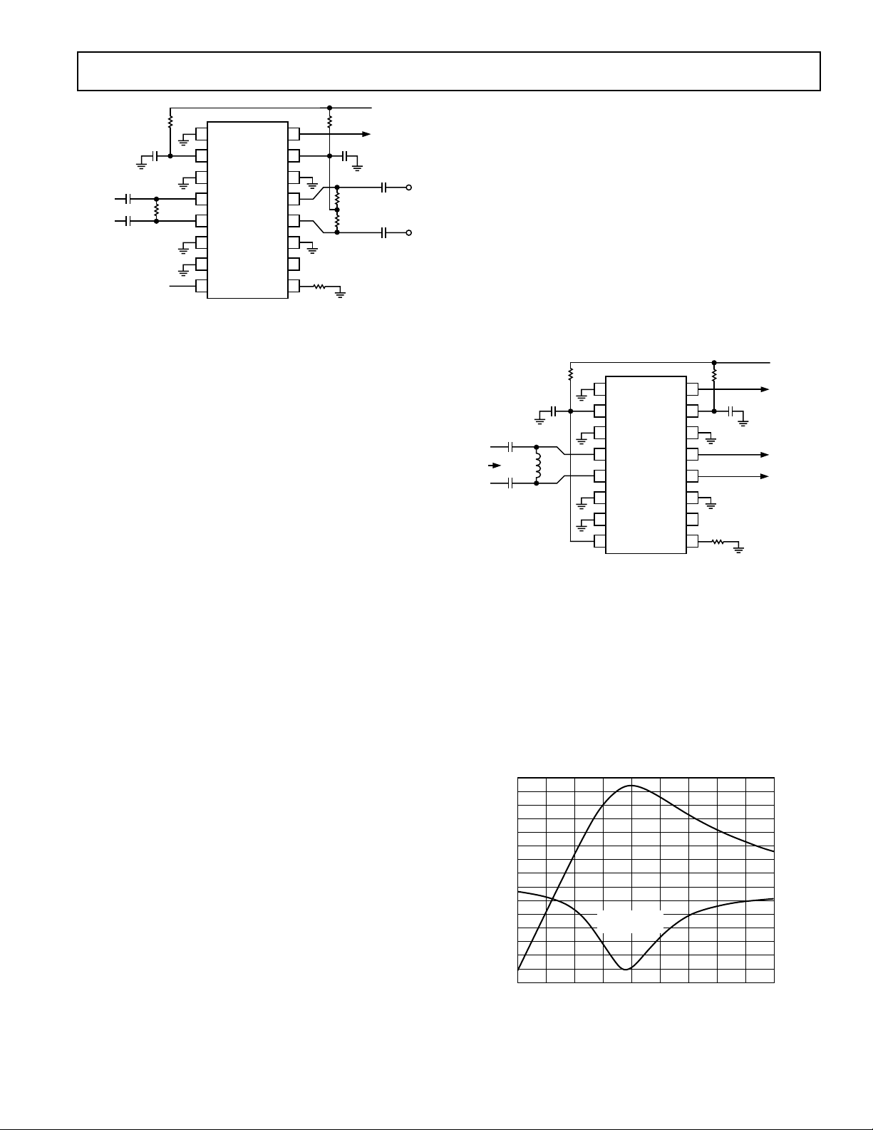
board, which fairly closely follows the basic connections schematic shown in Figure 27. For ordering information, please
refer to the Ordering Guide. Links, switches and component
settings for different setups are described in Table III.
REV. A
–13–
Page 14

AD8306
R3
0V
R4
R5
10V
(OPEN)
C5
0.01mF
L1
0.01mF
R12
0V
R11
0V
C6
(OPEN)
R9
+V
SIG
INHI
SIG
INLO
EXT
ENABLE
COM2
R2
R1
0V
10V
C1
0.01mF
C2
0.01mF
0.1mF
C3
R10
52.3V
A
BSW1
S
1
2
3
4
5
6
7
8
VPS1
PADL
INHI
INLO
PADL
COM1
ENBL
AD8306
VLOG
VPS2
PADL
LMHI
LMLO
PADL
FLTR
LMDR
16
15
14
13
12
11
10
9
R6
50V
C7 (OPEN)
LK1
0.1mF
402V
C4
R8
R7
50V
(OPEN)
Figure 33. Evaluation Board Schematic
Table III. Evaluation Board Setup Options
Component Function Default Condition
SW1 Device Enable. When in Position A, the ENBL pin is connected to +V
and the SW1 = A
S
AD8306 is in normal operating mode. In Position B, the ENBL pin is connected
to an SMA connector labeled Ext Enable. A signal can be applied to this connector
to enable/disable the AD8306.
R1 This pad is used to ac-couple INLO to ground for single-ended input drive. To drive R1 = 0 Ω
the AD8306 differentially, R1 should be removed.
R/L, C1, C2 Input Interface. The 52.3 Ω resistor in position R10, along with C1 and C2, create R10 = 52.3 Ω
a high-pass input filter whose corner frequency (640 kHz) is equal to 1/(2πRC), C1 = C2 = 0.01 µF
where C = (C1)/2 and R is the parallel combination of 52.3 Ω and the AD8306’s
input impedance of 1000 Ω. Alternatively, the 52.3 Ω resistor can be replaced by
an inductor to form an input matching network. See Input Matching Network
section for more details.
R3/R4 Slope Adjust. A simple slope adjustment can be implemented by adding a resistive R3 = 0 Ω
divider at the VLOG output. R3 and R4, whose sum should be about 1 kΩ, and R4 =
never less than 40 Ω (see specs), set the slope according to the equation:
Slope = 20 mV/dB × R4/(R3 + R4).
L1, C5, C6 Limiter Output Coupling. C5 and C6 ac-couple the limiter’s differential outputs. L1 = Open
By adjusting these values and installing an inductor in L1, an output matching C5 = 0.01 µF
network can be implemented. To convert the limiter’s differential output to single- C6 = 0.01 µF
ended, R11 and R12 (nominally 0 Ω) can be replaced with a surface mount balun R9 = Open
such as the ETC1-1-13 (Macom). The balun can be grounded by soldering a 0 Ω R10 = R11 = 0 Ω
into Position R9 (nominally open).
R8, LK1 Limiter Output Current. With LK1 installed, R8 enables and sets the limiter LK1 Installed. R8 = 402 Ω
output current. The limiter’s output current is set according to the equation R6, R7 (Limited Load
(I
= 400 mV/R8). The limiter current can be as high as 10 mA (R8 = 40 Ω). Resistors) = 50 Ω
OUT
To disable the limiter (recommended if the limiter is not being used), LK1 should
be removed.
C7 RSSI Bandwidth Adjust. The addition of C7 (farads) will lower the RSSI bandwidth of C7 = Open
the VLOG output according to the equation: f
(Hz) = 12.7 × 10⁻⁶/(C7 + 3.5 × 10
CORNER
–12
).
⬁
V
RSSI
+V
S
–14–
REV. A
Page 15
AD8306
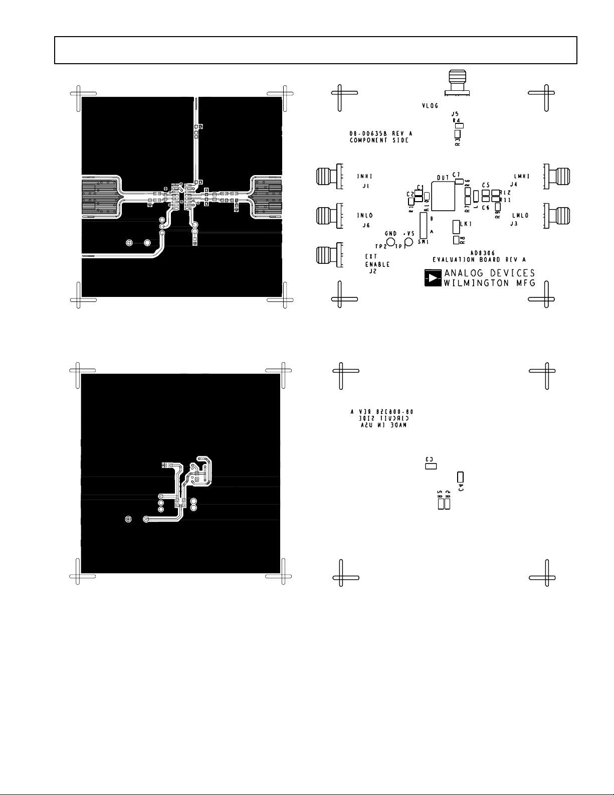
Figure 34. Layout of Signal Layer
Figure 35. Layout of Power Layer
Figure 36. Signal Layer Silkscreen
Figure 37. Power Layer Silkscreen
REV. A
–15–
Page 16

AD8306
0.1574 (4.00)
0.1497 (3.80)
PIN 1
OUTLINE DIMENSIONS
Dimensions shown in inches and (mm).
16-Lead Narrow Body SO
(SO-16)
0.3937 (10.00)
0.3859 (9.80)
16 9
0.050 (1.27)
BSC
0.2440 (6.20)
0.2284 (5.80)
81
0.0688 (1.75)
0.0532 (1.35)
0.0196 (0.50)
0.0099 (0.25)
C3592a–9–8/99
3 458
0.0098 (0.25)
0.0040 (0.10)
0.0192 (0.49)
0.0138 (0.35)
SEATING
PLANE
0.0099 (0.25)
0.0075 (0.19)
88
08
0.0500 (1.27)
0.0160 (0.41)
–16–
PRINTED IN U.S.A.
REV. A
 Loading...