

Page 1
D
A
C
A
R
E
G
I
S
T
E
R
D
PR
En
S
H
I
F
T
R
E
G
I
S
T
E
R
D
A
C
B
R
E
G
I
S
T
E
R
D
PR
R
E
F
E
R
E
N
C
E
B
A
N
D
G
A
P
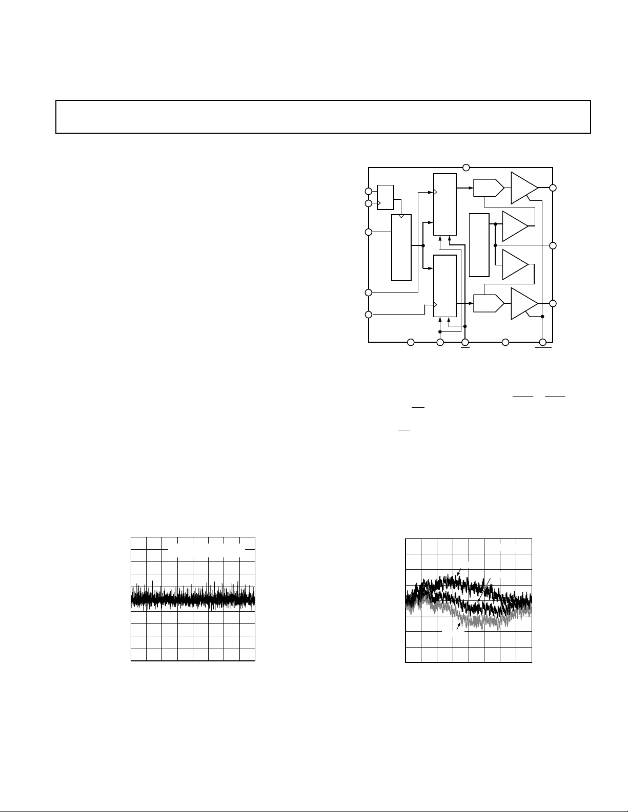
DAC A
DAC B
V
DD
REF
BUF
REF
BUF
AD8303
V
OUTA
V
REF
V
OUTB
CS
CLK
SDI
(DATA)
LDA
LDB
DGND MSB
RS
AGND
SHDN
OP
AMP
A
OP
AMP
B
+3 V, Dual, Serial Input
a
FEATURES
Complete Dual 12-Bit DAC
Pretrimmed Internal Voltage Reference
Single +3 V Operation
0.5 mV/Bit with 2.0475 V Full Scale
Low Power: 9.6 mW
3-Wire Serial SPI Compatible Interface
Power Shutdown I
Compact SO-14, 1.75 mm Height Package
APPLICATIONS
Portable Communications
Digitally Controlled Calibration
Servo Controls
PC Peripherals
DD
< 1 mA
Complete 12-Bit DAC
AD8303
FUNCTIONAL BLOCK DIAGRAM
GENERAL DESCRIPTION
The AD8303 is a complete (includes internal reference) dual,
12-bit, voltage output digital-to-analog converter designed to
operate from a single +3 volt supply. Built using a CBCMOS
process, this monolithic DAC offers the user low cost and easeof-use in single-supply +3 volt systems. Operation is guaranteed
over the supply voltage range of +2.7 V to +5.5 V making this
device ideal for battery operated applications.
The 2.0475 V full-scale voltage output is laser-trimmed to
maintain accuracy over the operating temperature range of the
device. The binary input data format provides an easy-to-use
one-half millivolt-per-bit software programmability. The voltage
outputs are capable of sourcing 3 mA.
1.0
0.8
0.6
0.4
0.2
0
–0.2
DNL – LSB
–0.4
–0.6
REV. 0
Information furnished by Analog Devices is believed to be accurate and
reliable. However, no responsibility is assumed by Analog Devices for its
use, nor for any infringements of patents or other rights of third parties
which may result from its use. No license is granted by implication or
–0.8
–1.0
Figure 1. Differential Nonlinearity Error vs. Code
0 4096
otherwise under any patent or patent rights of Analog Devices.
VDD = +5V
= –40°C, +25°C, +85°C
T
A
1024 2048 3072
DIGITAL INPUT CODE – Decimal
A double buffered serial data interface offers high speed, threewire, DSP and SPI microcontroller compatible inputs using
data in (SDI), clock (CLK) and load strobe (
pins. A chip-select (
CS) pin simplifies connection of multiple
LDA + LDB)
DAC packages by enabling the clock input when active low.
Additionally, an
RS input sets the output to zero scale or to 1/2
scale based on the level applied to the MSB pin. A power
shutdown feature reduces power dissipation to less than 3 µW.
The AD8303 is specified over the extended industrial (–40°C to
+85°C) temperature range. AD8303s are available in plastic
DIP and low profile 1.75 mm height SO-14 surface mount
packages. For single-channel DAC applications, see the
AD8300 which is offered in the 8-lead DIP and SO-8 packages.
2
1.5
1
0.5
0
–0.5
–1
INL LINEARITY ERROR – LSB
–1.5
–2
0 1024 2048 3072 4096
DIGITAL INPUT CODE – Decimal
–40°C
+85°C
VDD = +5V
+25°C
Figure 2. Linearity Error vs. Digital Code and Temperature
© Analog Devices, Inc., 1996
One Technology Way, P.O. Box 9106, Norwood, MA 02062-9106, U.S.A.
Tel: 617/329-4700 Fax: 617/326-8703
Page 2

AD8303–SPECIFICATIONS
+3 V OPERATION
(@ VDD = +2.7 V to +3.6 V, –408C ≤ TA ≤ +858C, unless otherwise noted)
Parameter Symbol Condition Min Typ1Max Units
STATIC PERFORMANCE
Resolution
Relative Accuracy
Differential Nonlinearity
Differential Nonlinearity
Zero-Scale Error V
Full-Scale Voltage
Full-Scale Tempco
2
2
2
2
3
3, 4
N 12 Bits
INL –2 ± 1/2 +2 LSB
DNL Monotonic, TA = +25°C –3/4 ±1/4 +3/4 LSB
DNL Monotonic –1 ±1/2 +1 LSB
ZSE
V
FS
TCV
FS
Data = 000
Data = FFF
H
2
H
1.25 +4.5 mV
2.039 2.0475 2.056 Volts
16 ppm/°C
ANALOG OUTPUTS
Output Current I
Output Resistance to GND R
Capacitive Load
4
OUT
C
OUT
L
Data = 800H, ∆V
Data = 000
H
No Oscillation
< 3 mV ±3mA
OUT
3
30 Ω
500 pF
REFERENCE OUTPUT
Output Voltage V
REF
Load > 1 MΩ 1V
LOGIC INPUTS
Logic Input Low Voltage V
Logic Input High Voltage V
Input Leakage Current I
Input Capacitance
4
INTERFACE TIMING SPECIFICATIONS
Clock Width High t
Clock Width Low t
Load Pulse Width t
Data Setup t
Data Hold t
Reset Pulse Width t
Load Setup t
Load Hold t
Select t
Deselect t
AC CHARACTERISTICS
Voltage Output Settling Time
Voltage Output Settling Time
4
6
6
Shutdown Recovery Time t
4, 5
IL
C
CH
CL
LDW
DS
DH
RS
LD1
LD2
CSS
CSH
t
S
t
S
DSR
IL
IH
IL
To ±0.1% of Full Scale 4 µs
To ±1 LSB of Final Value 14 µs
To ±0.1% of Full Scale 10 µs
Output Slew Rate SR Data = 000
to FFFH to 000
H
2.1 V
40 ns
40 ns
40 ns
15 ns
15 ns
40 ns
15 ns
40 ns
40 ns
40 ns
H
0.6 V
10 µA
10 pF
2.0 V/µs
DAC Glitch Q 15 nV/s
Digital Feedthrough Q 15 nV/s
SUPPLY CHARACTERISTICS
Power Supply Range V
Shutdown Current I
Supply Current
7
Power Dissipation P
DD RANGE
DD_SD
I
DD
DISS
DNL < ±1 LSB 2.7 5.5 V
SHDN = 0, No Load, VIL = 0 V, TA = +25°C 0.02 1 µA
V
= 3 V, VIL = 0 V, No Load 2 3.2 mA
DD
V
= 3 V, VIL = 0 V, No Load 6 9.6 mW
DD
Power Supply Sensitivity PSS ∆VDD = ±5% 0.001 0.004 %/%
NOTES
1
Typical readings represent the average value of room temperature operation.
2
1 LSB = 0.5 mV for 0 V to +2.0475 V output range. The first two codes (000H, 001H) are excluded from the linearity error measurement.
3
Includes internal voltage reference error.
4
These parameters are guaranteed by design and not subject to production testing.
5
All input control signals are specified with tR = tF = 2 ns (10% to 90% of +3 V) and timed from a voltage level of 1.6 V.
6
The settling time specification does not apply for negative going transitions within the last 6 LSBs of ground.
7
See Figure 6 for a plot of incremental supply current consumption as a function of the digital input voltage levels.
Specifications subject to change without notice.
REV. 0–2–
Page 3

SPECIFICATIONS
AD8303
+5 V OPERATION
(@ VDD = +5 V 6 10%, –408C ≤ TA ≤ +858C, unless otherwise noted)
Parameter Symbol Condition Min Typ1Max Units
STATIC PERFORMANCE
Resolution
Relative Accuracy
Differential Nonlinearity
Differential Nonlinearity
Zero-Scale Error V
Full-Scale Voltage
Full-Scale Tempco
2
2
2
2
3
3, 4
N 12 Bits
INL –2 ±1/2 +2 LSB
DNL Monotonic, TA = +25°C –3/4 ±1/4 +3/4 LSB
DNL Monotonic –1 ±1/2 +1 LSB
ZSE
V
FS
TCV
FS
Data = 000
Data = FFF
H
H
1.25 +4.5 mV
2.039 2.0475 2.056 Volts
16 ppm/°C
ANALOG OUTPUTS
Output Current I
Output Resistance to GND R
Capacitive Load
4
OUT
C
OUT
L
Data = 800H, ∆V
Data = 000
H
No Oscillation 500 pF
< 3 mV ±3mA
OUT
30 Ω
REFERENCE OUTPUT
Output Voltage V
REF
Load > 1 MΩ 1V
LOGIC INPUTS
Logic Input Low Voltage V
Logic Input High Voltage V
Input Leakage Current I
Input Capacitance
4
INTERFACE TIMING SPECIFICATIONS
Clock Width High t
Clock Width Low t
Load Pulse Width t
Data Setup t
Data Hold t
Reset Pulse Width t
Load Setup t
Load Hold t
Select t
Deselect t
AC CHARACTERISTICS
Voltage Output Settling Time
Voltage Output Settling Time
4
6
6
Shutdown Recovery Time t
4, 5
IL
C
CH
CL
LDW
DS
DH
RS
LD1
LD2
CSS
CSH
t
S
t
S
SDR
IL
IH
IL
To ±0.1% of Full Scale 4 µs
To ±1 LSB of Final Value
To ±0.1% of Full Scale 10 µs
Output Slew Rate SR Data = 000
to FFFH to 000
H
2.4 V
30 ns
30 ns
30 ns
15 ns
15 ns
30 ns
15 ns
30 ns
30 ns
30 ns
5
H
0.8 V
10 µA
10 pF
12 µs
2V/µs
DAC Glitch Q 15 nV s
Digital Feedthrough Q 15 nV s
SUPPLY CHARACTERISTICS
Power Supply Range V
Shutdown Supply Current I
Positive Supply Current
7
Power Dissipation P
DD RANGE
DD_SD
I
DD
DISS
DNL < ±1 LSB 2.7 3.0 5.5 V
SHDN = 0, No Load, VIL = 0 V, TA = +25°C 0.02 1 µA
V
= 5 V, VIL = 0 V, No Load 2.1 3.4 mA
DD
V
= 5 V, VIL = 0 V, No Load 10.5 17 mW
DD
Power Supply Sensitivity PSS ∆VDD = ±10% 0.001 0.004 %/%
NOTES
1
Typical readings represent the average value of room temperature operation.
2
1 LSB = 0.5 mV for 0 V to +2.0475 V output range. The first two codes (000H, 001H) are excluded from the linearity error measurement.
3
Includes internal voltage reference error.
4
These parameters are guaranteed by design and not subject to production testing.
5
All input control signals are specified with tR = tF = 2 ns (10% to 90% of +5 V) and timed from a voltage level of 1.6 V.
6
The settling time specification does not apply for negative going transitions within the last 6 LSBs of ground.
7
See Figure 6 for a plot of incremental supply current consumption as a function of the digital input voltage levels.
Specifications subject to change without notice.
REV. 0
–3–
Page 4

AD8303
WARNING!
ESD SENSITIVE DEVICE
ABSOLUTE MAXIMUM RATINGS*
VDD to GND . . . . . . . . . . . . . . . . . . . . . . . . . . . . . –0.3 V, +8 V
Logic Inputs to GND . . . . . . . . . . . . . . . . . . . . . .–0.3 V, +8 V
to GND . . . . . . . . . . . . . . . . . . . . . . –0.3 V, VDD + 0.3 V
V
OUT
Short Circuit to GND . . . . . . . . . . . . . . . . . . . . . . 50 mA
I
OUT
Package Power Dissipation . . . . . . . . . . . . . . . (T
Thermal Resistance θ
JA
J MAX–TA
)/θ
JA
14-Pin Plastic DIP Package (N-14) . . . . . . . . . . . . 103°C/W
14-Lead SOIC Package (R-14) . . . . . . . . . . . . . . . . 158°C/W
Maximum Junction Temperature (T
) . . . . . . . . . . . 150°C
J MAX
Operating Temperature Range . . . . . . . . . . . . –40°C to +85°C
Storage Temperature Range . . . . . . . . . . . . . –65°C to +150°C
Lead Temperature (Soldering, 10 secs) . . . . . . . . . . . . .+300°C
*Stress above those listed under “Absolute Maximum Ratings” may cause perma-
nent damage to the device. This is a stress rating only and functional operation of
the device at these or any other conditions above those indicated in the operational
sections of this specification is not implied. Exposure to absolute maximum rating
conditions for extended periods may affect device reliability.
SDI
CLK
CS
LDA, B
D11 D10 D9 D8 D7 D6 D5 D4 D3 D2 D1 D0
t
CSS
t
LD1
ORDERING GUIDE
Temperature Package Package
Model DNL Range Description Option
AD8303AN ±0.75 –40°C to +85°C 14-Pin P-DIP N-14
AD8303AR ±0.75 –40°C to +85°C 14-Lead SOIC R-14
The AD8303 contains 700 transistors. The die size measures 70 mil × 99 mil.
t
CSH
t
LD2
SDI
tDSt
DH
t
CLK
LDA, B
V
OUT
RS
FS
ZS
CL
t
CH
t
LDW
t
S
±1 LSB
ERROR BAND
a.
SHDN
I
DD
t
SDR
b.
Figure 3. Timing Diagrams
CAUTION
ESD (electrostatic discharge) sensitive device. Electrostatic charges as high as 4000 V readily
accumulate on the human body and test equipment and can discharge without detection.
Although the AD8303 features proprietary ESD protection circuitry, permanent damage may
occur on devices subjected to high energy electrostatic discharges. Therefore, proper ESD
precautions are recommended to avoid performance degradation or loss of functionality.
t
RS
t
S
REV. 0–4–
Page 5
AD8303
Table I. Control-Logic Truth Table
CS CLK RS MSB SHDN LDA/B Serial Shift Register Function DAC Register Function
H X H X H H No Effect Latched
L L H X H H No Effect Latched
L H H X H H No Effect Latched
L ↑+ H X H H Shift-Register-Data Advanced One Bit Latched
↑+ L H X H H No Effect Latched
HX H X H ↓– No Effect Updated with Current Shift Register Contents
H X H X H L No Effect Transparent
X X L H H X No Effect Loaded with 800
XX ↑+ H H H No Effect Latched with 800
X X L L H X No Effect Loaded with All Zeros
XX ↑+ X H H No Effect Latched All Zeros
X X X X L X No Effect No Effect
NOTES
1
↑+ positive logic transition; ↓– negative logic transition; X Don’t Care.
2
Do not clock in serial data while LDA or LDB is LOW.
PIN DESCRIPTIONS
Pin No. Name Function
1 AGND Analog Ground.
2V
OUTA
DAC voltage output, 2.0475 V full scale with 0.5 mV per bit. An internal temperature stabilized reference
maintains a fixed full-scale voltage independent of time, temperature and power supply variations.
3V
REF
Reference Voltage Output Terminal. Very high output resistance must be buffered if used as a virtual
ground.
4 DGND Digital Ground
5
CS Chip Select, Active Low Input. Disables shift register loading when high. Does not effect LDA or LDB
operation.
6 CLK Clock Input, positive edge clocks data into shift register.
7 SDI Serial Data Input, input data loads directly into the shift register.
8
LDA Load DAC register strobes, active low. Transfers shift register data to DAC A register. Asynchronous active
low input. See Control Logic Truth Table for operation.
9
10
RS Resets DAC register to zero condition or half-scale depending on MSB pin. Asynchronous active low input.
LDB Load DAC register strobes, active low. Transfers shift register data to DAC B register. Asynchronous active
low input. See Control Logic Truth Table for operation.
11 MSB Digital Input: Logic High presets DAC registers to half-scale 800
12
13 V
14 V
is strobed; Logic Low clears all DAC registers to zero (000
SHDN Active low shutdown control input. Does not affect register contents as long as power is present on VDD.
DD
OUTB
Positive power supply input. Specified range of operation +2.7 V to +5.5 V
DAC voltage output, 2.0475 V full scale with 0.5 mV per bit. An internal temperature stabilized reference
H
(sets MSB bit to one) when the RS pin
H
) when the RS pin is strobed.
maintains a fixed full-scale voltage independent of time, temperature and power supply variations.
H
H
PIN CONFIGURATION
14-Pin P-DIP (N-14)
14-Lead SOIC (R-14)
1
AGND
V
2
OUTA
V
3
REF
AD8303
TOP VIEW
4
DGND
CLK
SDI
CS
(Not to Scale)
5
6
7
REV. 0 –5–
14
V
OUTB
13
V
DD
SHDN
12
11
MSB
10
LDB
9
RS
LDA
8
Page 6

AD8303–Typical Performance Characteristics
7
6
0
01 534
3
5
4
2
LOGIC VOLTAGE – Volts
SUPPLY CURRENT – mA
VDD = +5V
VDD = +3V
TA = +25°C
DATA = 000
H
2
1
100
90
10
0%
1V 5µs
5V
V
OUT
LD
2.5
2.0
–0.5
1.5
1.0
0.5
0
–55 –35 1255 25 45 65 85 105–15
V
OUT
DRIFT – mV
TEMPERATURE – °C
VDD = +2.7V
VDD = +5.5V
NO LOAD
SS = 200 UNITS
NORMALIZED TO +25°C
120
80
40
0
–40
OUTPUT CURRENT – mA
–80
–120
75
60
45
30
15
POWER SUPPLY REJECTION – dB
0
10 100 1M10k 100k1k
POSITIVE
CURRENT
LIMIT
02
OUTPUT VOLTAGE – Volts
Figure 4. I
VDD = +3V ± 10%
OUT
VDD = +5V ± 10%
FREQUENCY – Hz
VDD = +5V
100
90
DATA = 800
RL TIED TO
+1.024V
NEGATIVE
CURRENT
LIMIT
1
vs. V
TA = +25°C
DATA = 800
OUT
H
10
0%
BROADBAND NOISE – 200µV/DIV
100
90
H
10
0%
TA = +25°C
NBW = 635kHz
Figure 5. Broadband Noise
50mV
V
OUT
LD
TIME = 100µs/DIV
CODE 800H TO 7FF
Figure 6. Supply Current vs. Logic
Input Voltage
200ns5V
H
Figure 7. Power Supply Rejection
vs. Frequency
10mV
100
90
V
OUT
10
0%
CLK
Figure 10. Clock Feedthrough vs.
Time
Figure 8. Midscale Transition
Figure 9. Large Signal Settling Time
Performance
120
100
80
60
FREQUENCY
40
1µs2V
20
0
–5 –3 1 5–1 9
TOTAL UNADJUSTED ERROR – LSB
Figure 11. Total Unadjusted
Error Histogram
TUE = ∑ (INL+ZS+FS)
SS = 200 UNITS
VDD = +2.7V
3 7 11 13 15
–6–
Figure 12. Full-Scale Voltage Drift
vs. Temperature
REV. 0
Page 7

AD8303
10
0%
100
90
V
OUT
500mV
1µs
5V
SHDN
2
1.5
–1
0 100 600200 300 500
0
0.5
1
–0.5
400
HOURS OF OPERATION AT +150°C
NOMINAL VOLTAGE CHANGE – mV
FULL SCALE
(DATA = FFF
H
)
ZERO SCALE
(DATA = 000
H
)
VDD = +2.7V
SS = 212 UNITS
70
60
0
–40 24–24 –16
50
–32
40
30
20
10
–8 8 160
TEMPERATURE COEFFICIENT – ppm/°C
FREQUENCY
V
DD
= +2.7V
SS = 200 UNITS
T
A
= –40 TO +85°C
10
0%
100
90
500mV
1µs
5V
V
OUT
SHDN
2.0
1.5
1.0
0.5
VDD = +4.5V
DRIFT – mV
OUT
0.0
V
–0.5
–1.0
–55 –35 1255 25 45 65 85 105–15
NO LOAD
SS = 200 UNITS
NORMALIZED TO +25°C
VDD = +2.7V
TEMPERATURE – °C
Figure 13. Zero-Scale Voltage Drift
vs. Temperature
30
25
20
15
10
SHUTDOWN CURRENT – nA
5
0
0 100 600200 300 500
HOURS OF OPERATION AT +150°C
VDD = +5V
SS = 212 UNITS
400
χ
+2σ
χ
χ
–2σ
10
V
= +5V
DD
DATA = FFF
1
OUTPUT VOLTAGE NOISE DENSITY – µV/Hz
0.1
1 100k10 100 1k 10k
FREQUENCY – Hz
H
Figure 14. Output Voltage Noise
Density vs. Frequency
6
V
= +5.5V,
DD
= 2.4V, DATA = FFF
V
LOGIC
5
V
= +3.6V,
DD
4
3
SUPPLY CURRENT – mA
DD
2
I
1
–60 –20 14020 60 100
= 2.1V, DATA = FFF
V
LOGIC
V
= +3.0V OR +5.0V,
DD
V
LOGIC
TEMPERATURE – °C
H
H
= 0V, DATA = 000
8040–40 0
H
120
Figure 15. Long-Term Drift
Accelerated by Burn-In
Figure 16. Shutdown Current vs.
Time Accelerated by Burn-In
1000
100
SHUTDOWN CURRENT – nA
DD
I
10
–55 125–35 –15 5
Figure 19. Shutdown Current vs.
Temperature
REV. 0 –7–
V
DD
TEMPERATURE – °C
= +5.5V
25 45 65 95 105
Figure 17. Supply Current vs.
Temperature
Figure 20. Shutdown Recovery Time
Figure 18. Full-Scale Output
Tempco Histogram
Figure 21. Shutdown Time
Page 8

AD8303
THEORY OF OPERATION
The AD8303 is a complete, ready-to-use, dual, 12-bit digital-toanalog converter. Only one +2.7 V to +5.5 V power supply is
necessary for operation. It contains two voltage-switched, 12-bit,
laser-trimmed digital-to-analog converters, a curvaturecorrected bandgap reference, rail-to-rail output op amps, input
shift register, and two DAC registers. The serial data interface
consists of a serial data input (SDI), clock (CLK), chip select
CS) and two DAC load strobe pins (LDA and LDB).
(
For battery operation and similar low power applications, a
shutdown feature (
SHDN) is available to reduce power supply
current to less than 1 µA. In addition an asynchronous reset pin
RS) will set both DAC outputs to either zero volts or to
(
midscale, depending on the logic value applied to the MSB pin.
This function is useful for power-on reset or system failure
recovery to a known state.
D/A CONVERTER SECTION
Each of the two DACs is a 12-bit device with an output that
swings from GND potential to 0.4 V generated from the internal
bandgap voltage (Figure 22). Each DAC uses a laser-trimmed
segmented R-2R ladder that is switched by n-channel
MOSFETs. The output voltage of the DAC has a constant
resistance independent of digital input code. The DAC output is
internally connected to the rail-to-rail output op amp.
OUTPUT SECTION
The rail-to-rail output stage of this amplifier has been designed
to provide precision performance while operating near either
power supply. Figure 23 shows an equivalent output schematic
of the rail-to-rail amplifier with its N-channel pull-down FETs
that will pull an output load directly to GND. The output
sourcing current is provided by a P-channel pull-up device that
can source current to GND terminated loads.
The rail-to-rail output stage permits operation at supply
voltages down to +2.7 V. The N-channel output pull-down
MOSFET shown in Figure 23 has a 35 Ω ON resistance which
sets the sink current capability near ground. In addition to
resistive load driving capability, the amplifier has also been
carefully designed and characterized for up to 500 pF capacitive
load driving capability.
V
P-CH
N-CH
DD
V
OUT
AGND
Figure 23. Equivalent Analog Output Circuit
V
BANDGAP
REF
2kΩ
1.0V 0.4V
10kΩ
12-BIT DAC
2.5kΩ
0.4V
FS
10kΩ
REF
1.0V
V
OUT
2.047V
FS
Figure 22. AD8303 Equivalent Schematic of Analog Section
AMPLIFIER SECTION
The internal DAC’s output is buffered by a low power
consumption, precision amplifier. This low power amplifier
contains a differential PNP pair input stage that provides low
offset voltage and low noise, as well as the ability to amplify the
zero-scale DAC output voltages, The rail-to-rail amplifier is
configured with a gain of approximately five in order to set the
2.0475 volt full-scale output (0.5 mV/LSB). An equivalent
circuit schematic for the amplifier section is shown in Figure 22.
The op amp has a 4 µs typical settling time to 0.1% of full scale.
There are slight differences in settling time for negative slewing
signals versus positive. Also, negative transition settling time to
within the last 6 LSBs of zero volts has an extended settling
time. See the oscilloscope photos in the typical performances
section of this data sheet.
REFERENCE SECTION
The internal curvature-corrected bandgap voltage reference is
laser trimmed for both initial accuracy and low temperature
coefficient. Figure 18 provides a histogram of total output
performance of full-scale versus temperature, which is dominated
by the reference performance.
V
Output
REF
The internal reference drives two resistor-divider networks. One
divider provides a 0.4 V reference for the DAC. The second
divider is trimmed to 1.0 V and is available at the V
output is useful for ratiometric applications, and also for
V
REF
pin. The
REF
generating a “false ground” or bipolar offset. See Figures 30
and Figure 31 for typical applications. Since V
has a high
REF
output impedance, it must be buffered if it is required to deliver
current to an external load.
REV. 0–8–
Page 9

AD8303
V
DD
LOGIC
IN
GND
POWER SUPPLY
The very low power consumption of the AD8303 is a direct
result of a circuit design optimizing the use of a CBCMOS
process. By using the low power characteristics of CMOS for
the logic, and the low noise, tight matching of the complementary
bipolar transistors, excellent analog accuracy is achieved.
One advantage of the rail-to-rail output amplifiers used in the
AD8303 is the wide range of usable supply voltage. The part is
fully specified and tested for operation from +2.7 V to +5.5 V.
If reduced linearity and source current capability near full scale
can be tolerated, operation of the AD8303 is possible down to
+2.7 V.
POWER SUPPLY BYPASSING AND GROUNDING
Precision analog products, such as the AD8303, require a well
filtered power source. Since the AD8303 operates from a single
+3 V to +5 V supply, it seems convenient to simply tap into the
digital logic power supply. Unfortunately, the logic supply is
often a switch-mode design, which generates noise in the
20 kHz to 1 MHz range. In addition, fast logic gates can
generate glitches hundred of millivolts in amplitude due to
wiring resistances and inductances. The power supply noise
generated thereby means that special care must be taken to
insure that the inherent precision of the DAC is maintained.
Good engineering judgment should be exercised when addressing
the power supply grounding and bypassing of the AD8303.
The AD8303 should be powered directly from the system power
supply. This arrangement, shown in Figure 24, employs an LC
filter and separate power and ground connections to isolate the
analog section from the logic switching transients. Analog and
digital ground pins of the AD8303 should be connected
together directly at the IC package.
Whether or not a separate power supply trace is available,
however, generous supply bypassing will reduce supply-line
induced errors. Local supply bypassing consisting of a 10 µF
tantalum electrolytic in parallel with a 0.1 µF ceramic capacitor
is recommended in all applications (Figure 25).
+2.7V TO +5.5V
13
7
SDI
CLK
LDA
LDB
MSB
SHDN
CS
RS
6
5
8
10
9
11
12
AGND DGND
AD8303
V
DD
TO ANALOG GROUND
2
14
41
0.1µF
10µF
V
V
OUTA
OUTB
Figure 25. Recommended Supply Bypassing for the
AD8303
INPUT LOGIC LEVELS
All digital inputs are protected with a Zener-type ESD protection
structure (Figure 26) that allows logic input voltages to exceed
the V
supply voltage. This feature can be useful if the user is
DD
driving one or more of the digital inputs with a 5 V CMOS logic
input voltage level while operating the AD8303 on a +3 V power
supply. If this mode of interface is used, make sure that the V
OL
of the 5 V CMOS meets the VIL input requirement of the
AD8303 operating at 3 V. See Figure 6 for a graph for digital
logic input threshold versus operating V
supply voltage.
DD
FERRITE BEAD:
2 TURNS, FAIR-RITE
#2677006301
0.1µF
CER.
+5V
+5V
RETURN
TTL/CMOS
LOGIC
CIRCUITS
+5V
POWER SUPPLY
100µF
ELECT.
10-22µF
TANT.
Figure 24. Use Separate Traces to Reduce Power Supply
Noise
Figure 26. Equivalent Digital Input ESD Protection
For power consumption-sensitive applications, it is important to
note that the internal power consumption of the AD8303 is
strongly dependent on the actual logic input voltage levels
present in the SDI, CLK,
CS, LDA, LDB, SHDN, RS and
MSB pins. Since these inputs are standard CMOS logic
structures, they contribute static power dissipation which
depends on the actual driving logic V
and VOL voltage levels.
OH
Consequently, using CMOS logic versus TTL will provide
minimal dissipation in the static state.
REV. 0 –9–
Page 10

AD8303
SDI
CLK
en
CS
12-BIT SHIFT
REGISTER
CLKDQ11–Q0
AD8303
12
LDA LDBMSB RS SHDN
Figure 27. AD8303 Digital Section Functional Block Diagram
DIGITAL INTERFACE
The AD8303 has a double-buffered serial data input. The
serial-input register is separate from the two DAC registers,
which allows preloading of a new data value into the serial
register without disturbing the present DAC values. A
functional block diagram of the digital section is shown in
Figure 27, while Table I contains the truth table for the control
logic inputs.
Three pins control the serial data input. Data at the Serial Data
Input (SDI) is clocked into the shift register on the rising edge
of CLK. Data is entered in MSB-first format. Twelve clock
pulses are required to load the 12-bit DAC value. If additional
bits are clocked into the shift register, for example when a µC
sends two 8-bit bytes, the MSBs are ignored (Figure 28). The
CLK pin is only enabled when Chip Select (
one AD8303 is connected to a serial data bus, then
CS) is low. If only
CS can be
tied (hardwired) to ground.
MSB LSB MSB LSB
B15 B14 B13 B12 B11 B10 B9 B8 B7 B6 B5 B4 B3 B2 B1 B0
X X X X D11 D10 D9 D8 D7 D6 D5 D4 D3 D2 D1 D0
D11–D0: 12-BIT DAC VALUE
X = DON'T CARE
THE MSB OF BYTE 1 IS THE FIRST BIT THAT IS LOADED INTO THE DAC
BYTE 1 BYTE 2
Figure 28. Typical AD8303-Microprocessor Serial Data
Input Format
MSB
DAC REGISTER A
RESET LOAD
MSB
DAC REGISTER B
RESET LOAD
12
DAC A
12
DAC B
V
V
OUTA
OUTB
Separate Load pins (LDA and LDB) are provided to control the
flow of data from the shift register to the DAC registers. After
the new value is loaded in the serial-input register, it can be
asynchronously transferred to either DAC register by strobing
the appropriate Load pin (
LDA or LDB). The Load pins are
level sensitive, so they should be returned high before any new
data is loaded into the serial-input register.
RESET (RS) AND MSB PINS
The RS pin forces both of the DAC registers to a known state,
based on the logic level on the MSB pin. If MSB is a logic zero,
then forcing
RS low will set the DAC latches to all zeros and the
DAC output voltage will be zero volts. If MSB is a logic one, then
RS will force the DAC latches to one-half scale (800H) and the
DAC outputs will be 1.024 V. The half-scale reset is useful for
systems where the DAC output is referenced to a “false
ground” (see the Generating Bipolar Outputs with a Single
Supply section of this data sheet for more information).
The reset function is useful for setting the DAC outputs to zero
at power-up or after a power supply interruption. Test systems
and motor controllers are two of many applications which
benefit from powering up to a known state. The reset pulse can
be generated by the microprocessor’s power-on RESET signal,
by an output from the microprocessor (Figure 33), or by an
external resistor and capacitor (Figure 34).
RS and MSB have level-sensitive thresholds. The RS input
overrides other logic inputs (specifically,
However,
high. If
LDA and LDB should be set high before RS goes
LDA or LDB are kept low, then the contents of the shift
register will be transferred to the DAC register as soon as
LDA and LDB).
RS
goes high.
REV. 0–10–
Page 11

AD8303
SHUTDOWN (SHDN)
The shutdown feature is activated when SHDN is pulled low.
While the AD8303 is in shutdown mode, the voltage reference,
DACs, and output amplifiers are all turned off. Supply current
is less than 1 µA. The DAC output voltage goes to 0 V, pulled
to GND by the 12.5 kΩ feedback resistors (Figure 22).
If power (i.e., V
) is maintained to the AD8303 during
DD
shutdown, the value stored in the DAC input latches will not
change. When the
SHDN pin is driven high, the DACs will
return to the same voltages as before shutdown. The CMOS
logic section of the AD8303 remains active while
SHDN is low.
Thus, new data can be loaded while the DACs are shut down
and, when
SHDN goes high, the DACs will assume the new
output voltage. The AD8303 recovers from shutdown very
quickly. The voltage output settling time after shutdown is
typically only a few microseconds longer than the normal
settling time (Figure 20).
+3V TO +5V
SDI
CLK
LDA
LDB
MSB
SHDN
CS
RS
7
6
5
8
10
9
11
12
13
V
DD
AD8303
V
OUTA
V
OUTB
AGND DGND
4
1
2, 14
14
0.1µF 10µF
2kΩ
0V ≤ V
500pF
V
OUT
OUTA
≤ 2.0475V
, V
OUTB
GENERATING “BIPOLAR” OUTPUTS WITH A SINGLE
SUPPLY
To maximize output signal swings in single supply operation,
many circuit designs employ a “false-ground” configuration.
This method defines a voltage, usually at one half of full scale or
at one half of the power supply, as the “ground” reference.
Signals are then measured differentially from the false ground,
which produces a “quasi-bipolar” output swing.
The AD8303’s voltage reference output, combined with an op
amp, can provide a temperature compensated false-ground
reference, as shown in Figure 30. The op amp amplifies the
AD8303’s 1.0 V reference by 1.024 to provide an analog
common (false ground) at one-half scale (1.024 V). With this
method, the DAC output is ± 1.024 V (referenced to the false
ground). The “Quasi-Bipolar” code table is given in Table III.
+3V
13
V
DD
AD8303
AGND DGND
V
41
OUTA
V
REF
2
3
+3V
OP193
0.022µF
R2A
97.6kΩ
R2B*
2kΩ
*ZERO-SCALE TRIM
R1
2.4kΩ
100Ω
V
= ±1.024V
OUT
(REFERENCED TO
SIGNAL GROUND)
SIGNAL GROUND
(FALSE GROUND, +1.024V)
1µF
Figure 29. Unipolar Output Operation
UNIPOLAR OUTPUT OPERATION
This is the basic mode of operation for the AD8303. As shown
in Figure 29, the AD8303 has been designed to drive loads as
low as 2 kΩ in parallel with 500 pF. The code table for this
operation is shown in Table II.
Table II. Unipolar Code Table
Hexadecimal Number Decimal Number Analog Output
in DAC Register in DAC Register Voltage (V)
FFF 4095 2.0475
801 2049 1.0245
800 2048 1.024
7FF 2047 1.0235
000 0 0
Figure 30. A False-Ground Generator
Table III. Quasi-Bipolar Code Table
DAC Analog
Hexadecimal Decimal Output Common “Bipolar”
Number Number In Voltage (False-Ground) Analog
in DAC Register DAC Register (V) Voltage (V) Voltage (V)
FFF 4095 2.0475 1.024 +1.2035
801 2049 1.0245 1.024 0.0005
800 2048 1.024 1.024 0
7FF 2047 1.0235 1.024 –0.0005
000 0 0 1.024 –1.024
Since the AD8303’s reference voltage output limits are typical, a
trim potentiometer is included so that the “false-ground” output
can be adjusted to exactly 1.024 V. To maintain accuracy,
resistors R1 and R2A must be of the same type (preferably
metal film) to insure temperature coefficient matching. The
circuit includes compensation to allow for a 1 µF bypass
capacitor at the false-ground output. The benefit of a large
capacitor is that not only does the false ground present a very
low dc resistance to the load, but its ac impedance is low as
well.
REV. 0 –11–
Page 12

AD8303
BIPOLAR OUTPUT OPERATION
Although the AD8303 has been designed for single-supply
operation, the output can also be configured for bipolar
operation. A typical circuit is shown in Figure 31. This circuit
uses the AD8303’s internal voltage reference to generate a
bipolar offset. Since V
must source current in this
REF
application, one half of an OP293 dual op amp is used as a
buffer. The other op amp then amplifies the DAC output
voltage to produce a bipolar output swing. The output voltage is
coded in offset binary and is given by:
V
= 0.5 mV × Digital Code ×
O
R3 + R4
R4
× 1 +
R2
R1
–1.0V ×
R2
R1
where 0.5 mV represents the pretrimmed value for one LSB of
the AD8303, Digital Code is the digital code sent to the DAC,
and 1.0 V is the AD8303 reference voltage.
+3V
7
6
5
8
10
9
11
12
13
V
SDI
CLK
CS
AD8303
LDA
LDB
RS
MSB
SHDN
AGND DGND
1
DD
3
V
REF
V
OUTA
V
OUTB
4
1/2
OP293
R3
10kΩ
2
14
19.08kΩ
R1
10kΩ
R4
R2
20.48kΩ
+3V
OP293
–3V
OPTIONAL
FULL-SCALE
TRIM
OPTIONAL
ZERO TRIM
1/2
V
OUT
= ±2.048V
Figure 31. Bipolar Output Operation
For a ±2.048 V full scale using the circuit values shown, the
transfer function becomes:
V
=1mV × Digital Code – 2.048V
O
Note that the full-scale span has increased from 2.048 V to
4.096 V (±2.048 V). Therefore, although each AD8303 LSB
represents 0.5 mV, each output LSB of the bipolar circuit has
been scaled to 1 mV. The code table for this circuit is shown in
Table IV.
Table IV. Bipolar Code Table
Hexadecimal Number Decimal Number Analog Output
in DAC Register in DAC Register Voltage (V)
FFF 4095 2.047
801 2049 0.001
800 2048 0
7FF 2047 –0.001
000 0 –2.048
important to maintain accuracy. Resistor pairs R1-R2 and
R3-R4 should be selected to match within 0.01%. In addition,
these resistors must be of the same type (preferably metal film)
to insure temperature coefficient matching. Mismatching
between R1 and R2 causes offset and gain errors while an R3 to
R4 mismatch yields gain errors.
GENERATING A NEGATIVE SUPPLY VOLTAGE
Some applications may require a bipolar output configuration,
as shown in Figure 31, but only have a single power supply rail
available. This is very common in data acquisition systems using
microprocessor-based systems. In these systems, +12 V, +15 V,
and/or +5 V only are available. Single supply rails are, of course,
common in battery-powered systems. Shown in Figure 32 is a
method of generating a negative supply using a single IC and
two capacitors. The ADM8660 employs a charge pump
technique to invert supply voltages as low as 1.5 V. A shutdown
feature on the ADM8660 complements the shutdown of the
AD8303. Note, however, that the ADM8660 requires about
500 µs to turn on after exiting the shutdown state.
+3V
8
2
CAP+
10µF
SHDN FROM AD8303
4
CAP–
V+
SHUTDOWN
GND
FC
1/6
74HC04
OSC
ADM8660
LV
61 3
5
7
–3V
10µF
Figure 32. Generating a Negative Supply Voltage
MICROCOMPUTER INTERFACES
The AD8303 serial data input provides an easy interface to a
variety of single-chip microcomputers (µCs). Many µCs have a
built-in serial data capability which can be used for communicating with the DAC. In cases where no serial port is provided,
or it is being used for some other purpose (such as an RS-232
communications interface), the AD8303 can easily be addressed
in software.
Twelve data bits are required to load a value into the AD8303.
If more than 12 bits are transmitted before the Chip Select
input goes high, the extra (i.e., the most significant) bits are
ignored. This feature is valuable because most µCs only transmit
data in 8-bit increments. Thus, the µC sends 16 bits to the DAC
instead of 12 bits. The AD8303 will only respond to the last 12
bits clocked into the SDI input, however, so the serial data
interface is not affected.
As with the false-ground generator circuit, resistor matching is
REV. 0–12–
Page 13

AD8303
AD8303-MC68HC11 INTERFACE
The circuit illustrated in Figure 33 shows a serial interface
between the AD8303 and the MC68HC11 8-bit microprocessor. The MOSI output drives the AD8303’s serial data
input, SDI, while SCK drives the clock (CLK). The DAC’s
CS,
LDA, LDB, MSB and RS inputs are driven by lines PD5 and
PC0–PC3, respectively.
(PD3) MOSI
(PD4) SCK
(PD5) SS
PC0
MC68HC11
NOTE: ADDITIONAL PINS OMITTED FOR CLARITY
PC1
PC2
PC3
SDI
CLK
CS
LDA
LDB
MSB
RS
AD8303
Figure 33. AD8303-MC68HC11 Serial Interface
To load data into the AD8303, the 68HC11’s CPOL and
CPHA bits are set high. This action configures the µC to
transfer data on the rising edge of the serial clock. After
CS is
set low, two bytes of data are sent to the AD8303 using the
format shown in Figure 28. Then
LDA or LDB are strobed low,
transferring the serial-input register contents to the appropriate
DAC. The
RS and MSB inputs allow the DAC to be reset to
either zero volts or half scale at any time.
AN 8051 µC INTERFACE
A typical interface between the AD8303 and an 8051 µC is
shown in Figure 34. This interface also uses the µC’s internal
serial port. The serial port is programmed for Mode 0
operation, which functions as a simple 8-bit shift register. The
8051’s Port 3.0 pin functions as the serial data output, while
Port 3.1 serves as the serial clock. The
LDA and LDB pins are
controlled by the 8051’s Port 1.0 and Port 1.1 lines, respectively.
P1.0
P1.1
DD
7
SDI
6
CLK
8
LDA
10
LDB
RS CS MSB SHDN
10k
9 5 11 12
+
1µF
AD8303
V
DD
(P3.0) RxD
(P3.1) TxD
80CL51
V
NOTE: ADDITIONAL PINS OMITTED FOR CLARITY
The 8051’s serial data transmission is straightforward. When
data is written to the serial buffer register (SBUF, at Special
Function Register location 99H), the data is automatically
converted to serial format and clocked out via Port 3.0 and Port
3.1 After 8 bits have been transmitted, the Transmit Interrupt
flag (SCON.1) is set and the next 8 bits can be transmitted.
The circuit of Figure 34 demonstrates “hardwiring” many of the
AD8303 features which may not have to be changed within a
given design. For example, the reset feature is controlled by a
resistor and capacitor. This produces a power-on reset pulse
without requiring a µC I/O pin. The MSB pin can be hardwired
or ground, depending on whether a reset to 0 V or half
to V
DD
scale is required. If the AD8303 is the only device on the serial
interface,
tied to V
CS can also be tied to ground. Finally, SHDN can be
if the shutdown feature will not be used.
DD
Software for the interface of Figure 34 is shown in Figure 35.
This routine sends the 12-bit value placed in registers
DAC_VAL0 and DAC_VAL1 to the DAC addressed by the two
LSBs of DAC_ADDR.
The subroutine begins by setting appropriate bits in the Serial
Control register to configure the serial port for Mode 0
operation. The MSBs of the DAC value are obtained from
memory location DAC_VAL1, adjusted to compensate for the
8051’s serial data format, and moved to the serial buffer
register. At this point, serial data transmission begins
automatically. When all 8 bits have been sent, the Transmit
Interrupt bit is set, and the subroutine then proceeds to send the
LSBs of the DAC value, stored at location DAC_VAL0. Next
LDA and LDB bits from DAC_ADDR are logically ANDed
the
with Port1. This action sets the appropriate AD8303 DAC
select input low and transfers the DAC value from the serialinput register to the DAC register, causing the DAC output
voltage to change. Finally the
LDA and LDB inputs are driven
high to await the next DAC update.
The 8051 sends data out of its shift register LSB first, while the
AD8303 requires data MSB first. The subroutine therefore
includes a BYTESWAP subroutine to reformat the data. This
routine transfers the MSB-first byte at location SHIFTREG to
an LSB-first byte at location SENDBYTE. The routine rotates
the MSB of the first byte into the carry with a Rotate Left Carry
instruction, then rotates the carry into the MSB of the second
byte with a Rotate Right Carry instruction. After 8 loops,
SENDBYTE contains the data in the proper format. The
BYTESWAP routine in Listing C is convenient because the
DAC data can be calculated in normal LSB form.
Figure 34. AD8303-80CL51 Serial Interface
REV. 0 –13–
Page 14

AD8303
;AD8303.ASM
;
; This subroutine loads an AD8303 shift register with a 12-bit
; DAC value, and transfers the value to DAC A or DAC B.
; The DAC value is stored at location DAC-VAL1 (MSB) and DAC_VAL0 (LSB)
; The DAC address (A or B) is stored at DAC_ADDR, (b0=0 for A, b1=0 for B)
;
; Primary controls
$MOD51
$TITLE(AD8303 Interface, Using the Serial Port in Mode 0)
;
; Variable declarations
;
PORT1 DATA 90H ;SFR register for port 1
DAC_VAL0 DATA 40H ;LSBs of 12-bit DAC Value
DAC_VAL1 DATA 41H ; MSBs of DAC Value
DAC_ADDR DATA 42H ;DAC address, format is:
; 1,1,1,1,1,1,LDB,LDA
; Set bit low to select DAC
LOOPCOUNT DATA 43H ;Count loops for byte swap
SHIFTREG DATA 44H ;Shift reg. for byte swap
SENDBYTE DATA 45H ; Destination reg. for SR
;
ORG 100H ;arbitrary starting address
DO_8303: CLR SCON.7 ;set serial
CLR SCON.6 ; data mode 0
CLR SCON.5 ;Clr SM2 for mode 0
CLR SCON.1 ;Clr the transmit flag
MOV SHIFTREG,DAC_VAL1 ;Get Most Significant Byte
ACALL SEND_IT ; send to AD8303
MOV SHIFTREG,DAC_VAL0 ;Get Least Significant Byte
ACALL SEND_IT ; send it to the AD8303
MOV A,PORT1 ;Get I/O port contents
ANL A,DAC_ADDR ;Clr LDA/LDB, other bits unchanged
MOV PORT1,A ;Send to I/O port
ORL A,#00000011B ;Set LDA and LDB high
MOV PORT1,A ;Send to I/O port
RET ;Done
;
;Convert the byte to LSB-first format and send it to the AD8303
SEND_IT: MOV LOOPCOUNT,#8 ;Shift 8 bits
BYTESWAP: MOV A,SHIFTREG ;Get source byte
RLC A ;rotate MSB to carry
MOV SHIFTREG,A ;Save new source byte
MOV A,SENDBYTE ;get destination byte
RRC A ;Move carry into MSB
MOV SENDBYTE,A ;Save
DJNZ LOOPCOUNT,BYTESWAP ;Done?
MOV SBUF,SENDBYTE ;Send the byte
SEND_WAIT: JNB SCON.1,SEND_WAIT ;Wait until 8 bits are send
CLR SCON.1 ;Clear the serial flag
RET ;Done
END
Figure 35. Software Listing for the AD8303-80CL51 Interface
REV. 0–14–
Page 15

0.210 (5.33)
MAX
0.200 (5.05)
0.125 (3.18)
OUTLINE DIMENSIONS
Dimensions shown in inches and (mm).
14-Lead Epoxy DIP (N-14)
0.795 (20.19)
0.725 (18.42)
14
17
PIN 1
0.022 (0.558)
0.014 (0.356)
0.100
(2.54)
BSC
8
0.280 (7.11)
0.240 (6.10)
0.060 (1.52)
0.015 (0.38)
0.070 (1.77)
0.045 (1.15)
0.150
(3.81)
MIN
SEATING
PLANE
0.325 (8.25)
0.300 (7.62)
14-Lead Narrow Body SOIC (R-14)
0.3444 (8.75)
0.3367 (8.55)
AD8303
0.195 (4.95)
0.115 (2.93)
0.015 (0.38)
0.008 (0.20)
0.1574 (4.00)
0.1497 (3.80)
0.0098 (0.25)
0.0040 (0.10)
SEATING
PLANE
14 8
PIN 1
0.0500
0.0192 (0.49)
(1.27)
0.0138 (0.35)
BSC
0.2440 (6.20)
71
0.2284 (5.80)
0.0688 (1.75)
0.0532 (1.35)
0.0099 (0.25)
0.0075 (0.19)
0.0196 (0.50)
0.0099 (0.25)
8°
0°
0.0500 (1.27)
0.0160 (0.41)
x 45°
REV. 0 –15–
Page 16

AD8303
C2098–18–1/96
PRINTED IN U.S.A.
REV. 0–16–
 Loading...