

Page 1
LF–2.7 GHz
MFLT
VMAG
MSET
PSET
VPHS
PFLT
VREF
VIDEO OUTPUT – A
INPA
OFSA
COMM
OFSB
INPB
VPOS
+
–+–
60dB LOG AMPS
(7 DETECTORS)
60dB LOG AMPS
(7 DETECTORS)
VIDEO OUTPUT – B
PHASE
DETECTOR
+
–
BIAS
x3
1.8V
AD8302
a
FEATURES
Measures Gain/Loss and Phase up to 2.7 GHz
Dual Demodulating Log Amps and Phase Detector
Input Range –60 dBm to 0 dBm in a 50 ⍀ System
Accurate Gain Measurement Scaling (30 mV/dB)
Typical Nonlinearity < 0.5 dB
Accurate Phase Measurement Scaling (10 mV/Degree)
Typical Nonlinearity < 1 Degree
Measurement/Controller/Level Comparator Modes
Operates from Supply Voltages of 2.7 V–5.5 V
Stable 1.8 V Reference Voltage Output
Small Signal Envelope Bandwidth from DC to 30 MHz
APPLICATIONS
RF/IF PA Linearization
Precise RF Power Control
Remote System Monitoring and Diagnostics
Return Loss/VSWR Measurements
Log Ratio Function for AC Signals
RF/IF Gain and Phase Detector
AD8302
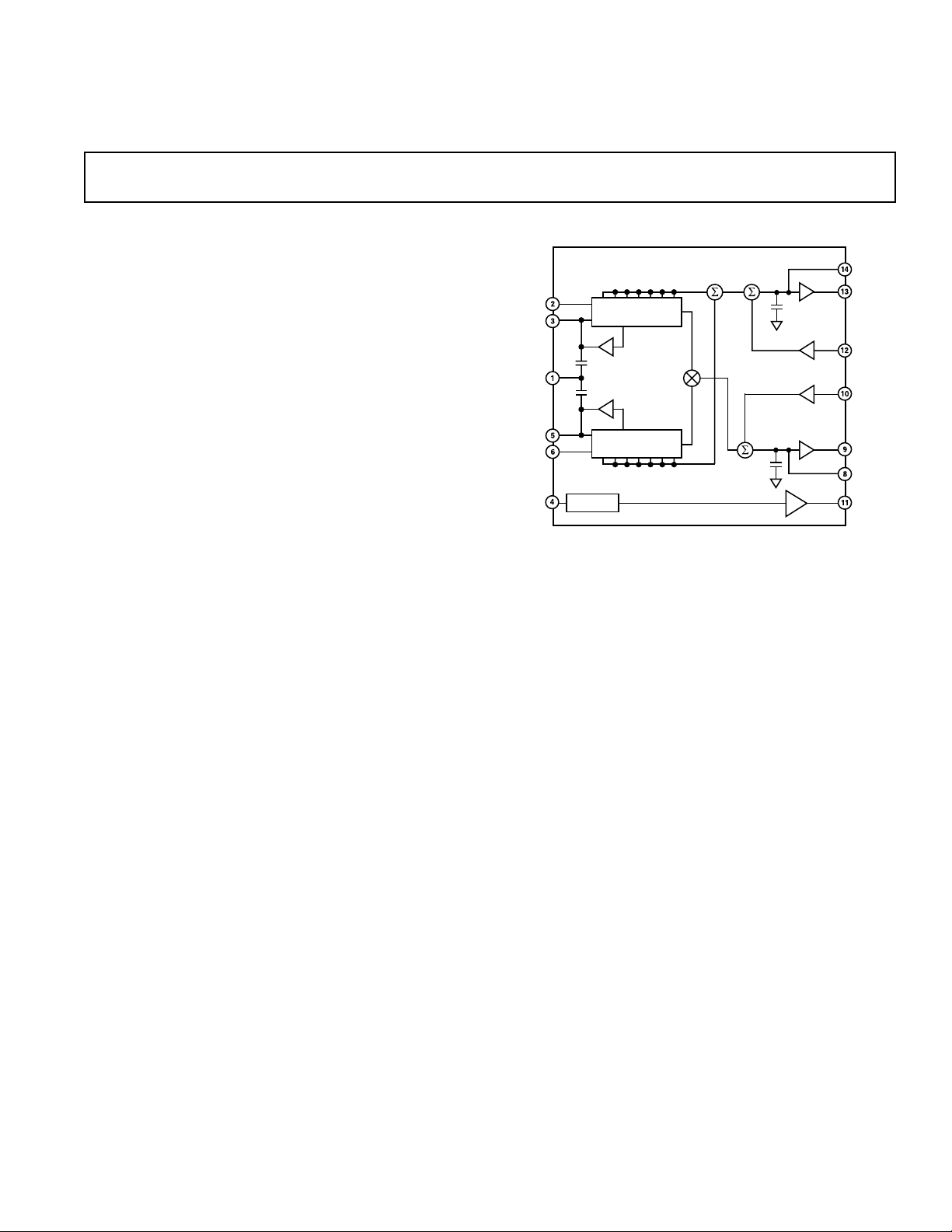
FUNCTIONAL BLOCK DIAGRAM
PRODUCT DESCRIPTION
The AD8302 is an innovative, fully integrated system for measuring gain/loss and phase in numerous receive, transmit, and
instrumentation applications. It requires few external components and a single supply of 2.7 V–5.5 V. The ac-coupled input
signals can range from –60 dBm to 0 dBm in a 50 Ω system, from
low frequencies up to 2.7 GHz. The outputs provide an accurate measurement of either gain or loss over a ±30 dB range
scaled to 30 mV/dB, and of phase over a 0°–180° range scaled to
10 mV/degree. Both subsystems have an output bandwidth of
30 MHz, which may optionally be reduced by the addition of
external filter capacitors. The AD8302 can be used in direct
control mode to servo gain and phase of a signal chain toward
predetermined setpoints.
The AD8302 comprises a closely matched pair of demodulating
logarithmic amplifiers, each having a 60 dB measurement range.
By taking the difference of their outputs, a measurement of
the magnitude ratio or gain between the two input signals is
available. These signals may even be at different frequencies,
allowing the measurement of conversion gain or loss. The AD8302
may be used to determine absolute signal level by applying the
unknown signal to one input and a calibrated ac reference signal
to the other. With the output stage feedback connection disabled, a comparator may be realized, using the setpoint pins
MSET and PSET to program the thresholds.
The signal inputs are single-ended, allowing them to be matched
and connected directly to a directional coupler. Their input
impedance is nominally 3 kΩ at low frequencies.
The AD8302 includes a phase detector of the multiplier type,
but with precise phase balance, driven by the fully limited signals appearing at the outputs of the two logarithmic amplifiers.
Thus, the phase accuracy measurement is independent of signal
level over a wide range.
The phase and gain output voltages are simultaneously available
at loadable ground referenced outputs over the standard output
range of 0 V to 1.8 V. The output drivers can source or sink up
to 8 mA. A loadable, stable reference voltage of 1.8 V is available for precise repositioning of the output range by the user.
In controller applications, the connection between the gain
output pin VMAG and the setpoint control pin MSET is broken.
The desired setpoint is presented to MSET and the VMAG
control signal drives an appropriate external variable gain device.
Likewise, the feedback path between the phase output pin VPHS
and its setpoint control pin PSET may be broken, to allow
operation as a phase controller.
The AD8302 is fabricated on Analog Devices’ proprietary, highperformance 25 GHz SOI complementary bipolar IC process. It is
available in a 14-lead TSSOP package and operates over a –40°C
to +85°C temperature range. An evaluation board is available.
REV. 0
Information furnished by Analog Devices is believed to be accurate and
reliable. However, no responsibility is assumed by Analog Devices for its
use, nor for any infringements of patents or other rights of third parties that
may result from its use. No license is granted by implication or otherwise
under any patent or patent rights of Analog Devices.
One Technology Way, P.O. Box 9106, Norwood, MA 02062-9106, U.S.A.
Tel: 781/329–4700 www.analog.com
Fax: 781/326-8703 © Analog Devices, Inc., 2001
Page 2

AD8302–SPECIFICATIONS
resistors connected to INPA and INPB, for Phase measurement P
(TA = 25ⴗC, VS = 5 V, VMAG shorted to MSET, VPHS shorted to PSET, 52.3 ⍀ shunt
= P
INPA
unless otherwise noted)
INPB
Parameter Conditions Min Typ Max Unit
OVERALL FUNCTION
Input Frequency Range >0 2700 MHz
Gain Measurement Range P
Phase Measurement Range φ
at INPA, PIN at INPB = –30 dBm ± 30 dB
IN
at INPA > φIN at INPB ± 90 Degree
IN
Reference Voltage Output Pin VREF, –40°C ≤ TA ≤ +85°C 1.72 1.8 1.88 V
INPUT INTERFACE Pins INPA and INPB
Input Simplified Equivalent Circuit To AC Ground, f ≤ 500 MHz 3储2kΩ储pF
Input Voltage Range AC-Coupled (0 dBV = 1 V rms) –73 –13 dBV
re: 50 Ω –60 0 dBm
Center of Input Dynamic Range –43 dBV
–30 dBm
MAGNITUDE OUTPUT Pin VMAG
Output Voltage Minimum 20 × Log (V
Output Voltage Maximum 20 × Log (V
Center Point of Output (MCP) V
INPA
= V
INPB
INPA/VINPB
INPA/VINPB
) = –30 dB 30 mV
) = +30 dB 1.8 V
900 mV
Output Current Source/Sink 8 mA
Small Signal Envelope Bandwidth Pin MFLT Open 30 MHz
Slew Rate 40 dB Change, Load 20 pF储10 kΩ 25 V/µs
Response Time
Rise Time Any 20 dB Change, 10%–90% 50 ns
Fall Time Any 20 dB Change, 90%–10% 60 ns
Settling Time Full-Scale 60 dB Change, to 1% Settling 300 ns
PHASE OUTPUT Pin VPHS
Output Voltage Minimum Phase Difference 180 Degrees 30 mV
Output Voltage Maximum Phase Difference 0 Degrees 1.8 V
= φ
Phase Center Point When φ
INPA
± 90° 900 mV
INPB
Output Current Drive Source/Sink 8 mA
Slew Rate 25 V/µs
Small Signal Envelope Bandwidth 30 MHz
Response Time Any 15 Degree Change, 10%–90% 40 ns
120 Degree Change C
= 1 pF, to 1% Settling 500 ns
FILT
100 MHz MAGNITUDE OUTPUT
Dynamic Range ± 1 dB Linearity P
± 0.5 dB Linearity P
± 0.2 dB Linearity P
= –30 dBm (V
REF
= –30 dBm (V
REF
= –30 dBm (V
REF
= –43 dBV) 58 dB
REF
= –43 dBV) 55 dB
REF
= –43 dBV) 42 dB
REF
Slope From Linear Regression 29 mV/dB
Deviation vs. Temperature Deviation from Output at 25°C
–40°C ≤ T
≤ +85°C, P
A
INPA
= P
= –30 dBm 0.25 dB
INPB
Deviation from Best Fit Curve at 25°C
Gain Measurement Balance P
–40°C ≤ T
= P
INPA
≤ +85°C, P
A
= –5 dBm to –50 dBm 0.2 dB
INPB
= ± 25 dB, P
INPA
= –30 dBm 0.25 dB
INPB
PHASE OUTPUT
Dynamic Range Less than ± 1 Degree Deviation from Best Fit Line 145 Degree
Less than 10% Deviation in Instantaneous Slope 143 Degree
Slope (Absolute Value) From Linear Regression about –90° or +90° 10 mV/Degree
Deviation vs. Temperature Deviation from Output at 25°C
–40°C ≤ T
≤ +85°C, Delta Phase = 90 Degrees 0.7 Degree
A
Deviation from Best Fit Curve at 25°C
–40°C ≤ TA ≤ +85°C, Delta Phase = ± 30 Degrees 0.7 Degree
–2–
REV. 0
Page 3

AD8302
Parameter Conditions Min Typ Max Unit
900 MHz MAGNITUDE OUTPUT
Dynamic Range ± 1 dB Linearity P
± 0.5 dB Linearity P
± 0.2 dB Linearity P
Slope From Linear Regression 28.7 mV/dB
Deviation vs. Temperature Deviation from Output at 25°C
–40°C ≤ T
≤ +85°C, P
A
Deviation from Best Fit Curve at 25°C
Gain Measurement Balance P
–40°C ≤ T
INPA
= P
≤ +85°C, P
A
INPB
PHASE OUTPUT
Dynamic Range Less than ± 1 Degree Deviation from Best Fit Line 143 Degree
Less than 10% Deviation in Instantaneous Slope 143 Degree
Slope (Absolute Value) From Linear Regression about –90° or +90° 10.1 mV/Degree
Deviation Linear Deviation from Best Fit Curve at 25°C
–40°C ≤ T
–40°C ≤ T
≤ +85°C, Delta Phase = 90 Degrees 0.75 Degree
A
≤ +85°C, Delta Phase = ± 30 Degrees 0.75 Degree
A
Phase Measurement Balance Phase @ INPA = Phase @ INPB, PIN = –5 dBm to –50 dBm 0.8
1900 MHz MAGNITUDE OUTPUT
Dynamic Range ± 1 dB Linearity P
± 0.5 dB Linearity P
± 0.2 dB Linearity P
Slope From Linear Regression 27.5 mV/dB
Deviation vs. Temperature Deviation from Output at 25°C
–40°C ≤ T
≤ +85°C, P
A
Deviation from Best Fit Curve at 25°C
Gain Measurement Balance P
–40°C ≤ T
INPA
= P
≤ +85°C, P
A
INPB
PHASE OUTPUT
Dynamic Range Less than ± 1 Degree Deviation from Best Fit Line 128 Degree
Less than 10% Deviation in Instantaneous Slope 120 Degree
Slope (Absolute Value) From Linear Regression about –90° or +90° 10.2 mV/Degree
Deviation Linear Deviation from Best Fit Curve at 25°C
–40°C ≤ T
–40°C ≤ T
≤ +85°C, Delta Phase = 90 Degrees 0.8 Degree
A
≤ +85°C, Delta Phase = ± 30 Degrees 0.8 Degree
A
Phase Measurement Balance Phase @ INPA = Phase @ INPB, PIN = –5 dBm to –50 dBm 1 Degree
2200 MHz MAGNITUDE OUTPUT
Dynamic Range ± 1 dB Linearity P
± 0.5 dB Linearity P
± 0.2 dB Linearity P
Slope From Linear Regression 27.5 mV/dB
Deviation vs. Temperature Deviation from Output at 25°C
–40°C ≤ T
≤ +85°C, P
A
Deviation from Best Fit Curve at 25°C
Gain Measurement Balance P
–40°C ≤ T
INPA
= P
≤ +85°C, P
A
INPB
PHASE OUTPUT
Dynamic Range Less than ± 1 Degree Deviation from Best Fit Line 115 Degree
Less than 10% Deviation in Instantaneous Slope 110 Degree
Slope (Absolute Value) From Linear Regression about –90° or +90° 10 mV/Degree
Deviation Linear Deviation from Best Fit Curve at 25°C
–40°C ≤ T
≤ +85°C, Delta Phase = 90 Degrees 0.85 Degree
A
–40°C ≤ TA ≤ +85°C, Delta Phase = ± 30 Degrees 0.9 Degree
REFERENCE VOLTAGE Pin VREF
Output Voltage Load = 2 kΩ 1.7 1.8 1.9 V
PSRR V
= 2.7 V to 5.5 V 0.25 mV/V
S
Output Current Source/Sink (Less than 1% Change) 5 mA
POWER SUPPLY Pin VPOS
Supply 2.7 5.0 5.5 V
Operating Current (Quiescent) V
= 5 V 19 25 mA
S
–40°C ≤ TA ≤ +85°C2127mA
Specifications subject to change without notice.
= –30 dBm (V
REF
= –30 dBm (V
REF
= –30 dBm (V
REF
= P
INPA
= ± 25 dB, P
INPA
= –43 dBV) 58 dB
REF
= –43 dBV) 54 dB
REF
= –43 dBV) 42 dB
REF
= –30 dBm 0.25 dB
INPB
= –30 dBm 0.25 dB
INPB
= –5 dBm to –50 dBm 0.2 dB
Degree
= –30 dBm (V
REF
= –30 dBm (V
REF
= –30 dBm (V
REF
= P
INPA
= ±25 dB, P
INPA
= –5 dBm to –50 dBm 0.2 dB
= –30 dBm (V
REF
= –30 dBm (V
REF
= –30 dBm (V
REF
= P
INPA
= ± 25 dB, P
INPA
= –5 dBm to –50 dBm 0.2 dB
= –43 dBV) 57 dB
REF
= –43 dBV) 54 dB
REF
= –43 dBV) 42 dB
REF
= –30 dBm 0.27 dB
INPB
= –30 dBm 0.33 dB
INPB
= –43 dBV) 53 dB
REF
= –43 dBV) 51 dB
REF
= –43 dBV) 38 dB
REF
= –30 dBm 0.28 dB
INPB
= –30 dBm 0.4 dB
INPB
REV. 0
–3–
Page 4

AD8302
TOP VIEW
(Not to Scale)
1
COMM
AD8302
INPA
OFSA
VPOS
OFSB
INPB
COMM
MFLT
VMAG
MSET
VREF
PSET
VPHS
PFLT
2
3
4
5
6
7
14
13
12
11
10
9
8
WARNING!
ESD SENSITIVE DEVICE
ABSOLUTE MAXIMUM RATINGS
1
PIN CONFIGURATION
Supply Voltage VS . . . . . . . . . . . . . . . . . . . . . . . . . . . . . 5.5 V
PSET, MSET Voltage . . . . . . . . . . . . . . . . . . . . . . V
+ 0.3 V
S
INPA, INPB Maximum Input . . . . . . . . . . . . . . . . . . –3 dBV
Equivalent Power Re. 50 Ω . . . . . . . . . . . . . . . . . . 10 dBm
2
. . . . . . . . . . . . . . . . . . . . . . . . . . . . . . . . . . . . . 150°C/W
θ
JA
Maximum Junction Temperature . . . . . . . . . . . . . . . . 125°C
Operating Temperature Range . . . . . . . . . . . –40°C to +85°C
Storage Temperature Range . . . . . . . . . . . . –65°C to +150°C
Lead Temperature Range (Soldering 60 sec) . . . . . . . . 300°C
NOTES
1
Stresses above those listed under Absolute Maximum Ratings may cause permanent damage to the device. This is a stress rating only; functional operation of the
device at these or any other conditions above those indicated in the operational
section of this specification is not implied. Exposure to absolute maximum rating
conditions for extended periods may affect device reliability.
2
JEDEC 1S Standard (2-layer) board data.
PIN FUNCTION DESCRIPTIONS
Equivalent
Pin No. Mnemonic Function Circuit
1, 7 COMM Device Common. Connect to low impedance ground.
2 INPA High Input Impedance to Channel A. Must be ac-coupled. Circuit A
3 OFSA A capacitor to ground at this pin sets the offset compensation filter corner Circuit A
and provides input decoupling.
4 VPOS Voltage Supply (V
), 2.7 V to 5.5 V.
S
5 OFSB A capacitor to ground at this pin sets the offset compensation filter corner Circuit A
and provides input decoupling.
6 INPB Input to Channel B. Same structure as INPA. Circuit A
8 PFLT Low-Pass Filter Terminal for the Phase Output. Circuit E
9 VPHS Single-Ended Output Proportional to the Phase Difference between INPA Circuit B
and INPB.
10 PSET Feedback Pin for Scaling of VPHS Output Voltage in Measurement Mode. Circuit D
Apply a setpoint voltage for controller mode.
11 VREF Internally-Generated Reference Voltage (1.8 V Nominal). Circuit C
12 MSET Feedback Pin for Scaling of VMAG Output Voltage Measurement Mode. Circuit D
Accepts a set point voltage in controller mode.
13 VMAG Single-Ended Output. Output voltage proportional to the decibel ratio
of signals applied to INPA and INPB. Circuit B
14 MFLT Low-Pass Filter Terminal for the Magnitude Output. Circuit E
CAUTION
ESD (electrostatic discharge) sensitive device. Electrostatic charges as high as 4000 V readily
accumulate on the human body and test equipment and can discharge without detection. Although
the AD8302 features proprietary ESD protection circuitry, permanent damage may occur on
devices subjected to high-energy electrostatic discharges. Therefore, proper ESD precautions are
recommended to avoid performance degradation or loss of functionality.
ORDERING GUIDE
Package
Model Temperature Range Package Description Option
AD8302ARU –40°C to +85°C Tube, 14-Lead TSSOP RU-14
AD8302ARU-REEL 13" Tape and Reel
AD8302ARU-REEL7 7" Tape and Reel
AD8302-EVAL Evaluation Board
–4–
REV. 0
Page 5

AD8302
INPA(INPB)
OFSA(OFSB)
VPOS
COMM
10k⍀
5k⍀
Circuit C
100mV
4k⍀
4k⍀
10pF
COMM
Circuit A
VREF
VPOS
+
ON TO
LOG-AMP
–
MSET
(PSET)
VPOS
10k⍀
10k⍀
COMM
Circuit D
ACTIVE LOADS
750⍀
2k⍀
VPOS
CLASS A-B
CONTROL
COMM
Circuit B
25⍀
VPOS
COMM
Circuit E
VMAG
(VPHS)
MFLT
(PFLT)
1.5pF
Figure 1. Equivalent Circuits
REV. 0
–5–
Page 6
AD8302
Typical Performance Characteristics
(VS = 5 V, V
is the reference input and V
INPB
is swept unless otherwise
INPA
noted. All references to dBm are referred to 50 ⍀. For the Phase Output curves the input signal levels are equal unless otherwise noted.)
VMAG – dB
VMAG – dB
1.80
1.65
1.50
1.35
1.20
1.05
0.90
0.75
0.60
0.45
0.30
0.15
1.80
1.65
1.50
1.35
1.20
1.02
0.90
0.75
0.60
0.45
0.30
0.15
0
–30
0
–30
–20 –10 0 10 20 30
–20 –10 0 10 20 30
MAGNITUDE RATIO – dB
°
C, +25°C, and +85°C,
MAGNITUDE RATIO – dB
°
C, +25°C, and +85°C,
3.0
2.5
2.0
1.5
1.0
0.5
0.0
–0.5
–1.0
–1.5
–2.0
–2.5
–3.0
3.0
2.5
2.0
1.5
1.0
0.5
0.0
–0.5
–1.0
–1.5
–2.0
–2.5
–3.0
2.0
1.8
1.6
1.4
1.2
1.0
VMAG – V
0.8
0.6
0.4
0.2
0
–25 –20 –15 –10 –5 0 5 1015202530
–30
MAGNITUDE RATIO – dB
100
2700
900
2200
1900
TPC 1. Magnitude Output (VMAG) vs. Input Level Ratio
(Gain) V
INPA/VINPB
1900 MHz, 2200 MHz, 2700 MHz, 25
Ω
(Re: 50
)
2.0
1.8
1.6
1.4
1.2
1.0
VMAG – V
0.8
0.6
0.4
0.2
0
–30
TPC 2. VMAG vs. Input Level Ratio (Gain) V
, Frequencies 100 MHz, 900 MHz,
°
C, P
1900
2700
–25 –20 –15 –10 –5 0 5 1015202530
MAGNITUDE RATIO – dB
= –30 dBm,
INPB
2200
900
100
INPA/VINPB
,
Frequencies 100 MHz, 900 MHz, 1900 MHz, 2200 MHz,
2700 MHz, P
= –30 dBm
INPA
TPC 4. VMAG and Log Conformance vs. Input Level Ratio
(Gain), Frequency 900 MHz, –40
Reference Level = –30 dBm
TPC 5. VMAG and Log Conformance vs. Input Level Ratio
(Gain), Frequency 1900 MHz, –40
Reference Level = –30 dBm
ERROR IN VMAG – dB
ERROR IN VMAG – dB
1.80
1.65
1.50
1.35
1.20
1.05
0.90
VMAG – V
0.75
0.60
0.45
0.30
0.15
0
–30
–20 –100 102030
MAGNITUDE RATIO – dB
TPC 3. VMAG Output and Log Conformance vs. Input
Level Ratio (Gain), Frequency 100 MHz, –40
°
and +85
C, Reference Level = –30 dBm
°
C, +25°C,
3.0
2.5
2.0
1.5
1.0
0.5
0.0
–0.5
–1.0
–1.5
–2.0
–2.5
–3.0
1.80
1.65
1.50
1.35
1.20
1.02
0.90
0.75
VMAG – dB
ERROR IN VMAG – dB
0.60
0.45
0.30
0.15
0
–30
–20 –10 0 10 20 30
MAGNITUDE RATIO – dB
TPC 6. VMAG Output and Log Conformance vs. Input
Level Ratio (Gain), Frequency 2200 MHz, –40
°
and +85
C, Reference Level = –30 dBm
–6–
°
C, +25°C,
3.0
2.5
2.0
1.5
1.0
0.5
0.0
–0.5
–1.0
ERROR IN VMAG – dB
–1.5
–2.0
–2.5
–3.0
REV. 0
Page 7

AD8302
3.0
2.5
2.0
1.5
1.0
0.5
0.0
–0.5
–1.0
ERROR IN VMAG – dB
–1.5
–2.0
–2.5
–3.0
–25 –20 –15 –10 –5 0 5 1015202530
–30
+85 C
+85 C
–40 C
MAGNITUDE RATIO – dB
–40 C
+25 C
TPC 7. Distribution of Magnitude Error vs. Input Level
Ratio (Gain), Three Sigma to Either Side of Mean, Fre-
°
quency 900 MHz, Temperatures –40
C, +25°C, and +85°C,
Reference Level = –30 dBm
3.0
2.5
2.0
1.5
1.0
0.5
0.0
–0.5
–1.0
ERROR IN VMAG – dB
+25 C
–1.5
–2.0
–2.5
–3.0
–25 –20 –15 –10 –5 0 5 1015202530
–30
–40 C
MAGNITUDE RATIO – dB
–40 C
+85 C
+85 C
2.0
1.8
1.6
1.4
1.2
1.0
VMAG – V
0.8
0.6
0.4
0.2
0.0
–30
–25 –20 –15 –10 –5 0 5 1015202530
MAGNITUDE RATIO – dB
TPC 10. Distribution of VMAG vs. Input Level Ratio (Gain),
Three Sigma to Either Side of Mean, Frequency 1900 MHz,
°
Temperatures Between –40
C, and +85°C, Reference Level
= –30 dBm
–30dBm
3.0
2.5
2.0
1.5
1.0
0.5
0.0
–0.5
–1.0
–1.5
–2.0
–2.5
–3.0
ERROR IN VMAG – dB
1.8
1.6
1.4
1.2
1.0
0.8
VMAG – V
–30dBm
0.6
0.4
0.2
0.0
–30
–45dBm
–15dBm
–20 –100 102030
MAGNITUDE RATIO – dB
–40dBm
–15dBm
TPC 8. Distribution of Error vs. Input Level Ratio (Gain),
Three Sigma to Either Side of Mean, Frequency 1900 MHz,
°
C, +25°C, and +85°C, Reference Level = –30 dBm
–40
3.0
2.5
2.0
1.5
1.0
0.5
0.0
–0.5
–1.0
ERROR IN VMAG – dB
–1.5
–2.0
–2.5
–3.0
–30
+25 C
–25 –20 –15 –10 –5 0 5 1015202530
–40 C
+85 C
+85 C
–40 C
MAGNITUDE RATIO – dB
TPC 9. Distribution of Magnitude Error vs. Input Level
Ratio (Gain), Three Sigma to Either Side of Mean, Frequency 2200 MHz, Temperatures –40°C, +25°C, and +85°C,
Reference Level = –30 dBm
REV. 0
TPC 11. VMAG Output and Log Conformance vs. Input
Level Ratio (Gain), Reference Level = –10 dBm, –30 dBm,
and –45 dBm, Frequency 1900 MHz
1.10
P
= P
1.05
1.00
0.95
0.90
VMAG – V
0.85
0.80
0.75
–65
–60 –55 –50 –45 –40 –35 –30
INPA
P
INPA
P
INPA
INPUT LEVEL – dBm
TPC 12. VMAG Output vs. Input Level for P
P
INPA
= P
+5 dB, P
INPB
INPA
= P
+ 5dB
INPB
= P
INPB
= P
– 5dB
INPB
–25 –20 –15 –10 –50
–5 dB, Frequency 1900 MHz
INPB
INPA
= P
–7–
INPB
,
Page 8

AD8302
1.06
1.04
1.02
1.00
0.98
0.96
0.94
0.92
0.90
0.88
VMAG – V
0.86
0.84
0.82
0.80
0.78
0.76
0.74
200 400 600 800 1000 1200 1400
TPC 13. VMAG Output vs. Frequency, for P
P
INPA
= P
CHANGE IN SLOPE – mV
+5 dB, and P
INPB
0.4
0.2
0
–0.2
–0.4
–0.6
–0.8
–1.0
–1.2
–1.4
–1.6
–1.8
–40 –200 20406080
P
= P
INPA
INPB
P
= P
INPA
P
= P
INPA
INPB
FREQUENCY – MHz
= P
INPA
TEMPERATURE – ⴗC
INPB
+ 5dB
INPB
– 5dB
1600 1800 2000 22000
–5 dB, P
= P
INPA
= 30 dBm
INPB
85
INPB
,
TPC 14. Change in VMAG Slope vs. Temperature, Three
Sigma to Either Side of Mean, Frequencies 1900 MHz
18
15
12
9
PERCENT
6
3
0
0.80 0.85 0.90
MCP – V
0.95
1.00
TPC 16. Center Point of Magnitude Output (MCP) Distribution Frequencies 900 MHz, 17,000 Units
18
15
12
9
PERCENT
6
3
0
27.0 27.5 28.0 28.5
VMAG SLOPE – mV/dB
29.0
29.5 30.0
TPC 17. VMAG Slope, Frequency 900 MHz, 17,000 Units
25
20
15
10
5
0
–5
VMAG – mV
–10
–15
–20
–25
–40 –30 –20 –10 0 10 20
TEMPERATURE – ⴗC
30 40 50 60
70 80 90
TPC 15. Change in Center Point of Magnitude Output
(MCP) vs. Temperature, Three Sigma to Either Side of
Mean Frequencies 1900 MHz
–8–
0.032
0.030
0.028
SLOPE OF VMAG – V
0.026
0.024
0
200
400
600
800
1000
1200
1400
FREQUENCY – MHz
TPC 18. VMAG Slope vs. Frequency
1600
1800
2000
2200
2400
2600
REV. 0
2800
Page 9

25ns
FREQUENCY – Hz
VMAG – nV/ Hz
1k 10k
10000
100k 1M 10M 100M
1000
100
10
INPUT –50dBm
INPUT –30dBm
INPUT –10dBm
FREQUENCY – Hz
VMAG – nV/ Hz
1k 10k
10000
100k 1M 10M 100M
1000
100
10
INPUT –50dBm
INPUT –30dBm
INPUT –10dBm
HORIZONTAL
20mV PER
VERTICAL
DIVISION
AD8302
TPC 19. Magnitude Output Response to 4 dB Step, for
P
= –30 dBm, P
INPB
= –32 dBm to –28 dBm, Frequency
INPA
1900 MHz, No Filter Capacitor
20mV PER
VERTICAL
DIVISION
1.00s
HORIZONTAL
TPC 20. Magnitude Output Response to 4 dB Step, for
= –30 dBm, P
P
INPB
= –32 dBm to –28 dBm, Frequency
INPA
1900 MHz, 1 nF Filter Capacitor
200mV PER
VERTICAL
DIVISION
100ns
TPC 21. Magnitude Output Response to 40 dB Step, for
P
INPB
Frequency 1900 MHz, No Filter Capacitor
= –30 dBm, P
INPA
HORIZONTAL
= –50 dBm to –10 dBm, Supply 5 V,
TPC 22. Magnitude Output Noise Spectral
Density, P
INPA
= P
= –10 dBm, –30 dBm,
INPB
–50 dBm, No Filter Capacitor
TPC 23. Magnitude Output Noise Spectral Density, P
= –10 dBm, –30 dBm, –50 dBm, with Filter Capacitor
P
INPB
0.18
0.16
0.14
0.12
0.10
0.08
0.06
VMAG (PEAK-TO-PEAK) – V
0.04
0.02
0.00
1900
900
100
–25 –20
2700
1200
–15 –10 25–5 0 5 101520
MAGNITUDE RATIO – dB
INPA
=
TPC 24. VMAG Peak-to-Peak Output Induced by Sweeping
Phase Difference through 360 Degrees vs. Magnitude Ratio,
Frequencies 100 MHz, 900 MHz, 1900 MHz, 2200 MHz
REV. 0
–9–
Page 10

AD8302
1.8
1.6
1.4
1.2
1.0
0.8
PHASE OUT – V
0.6
0.4
0.2
0.0
–180 –140
100MHz
190MHz
2200MHz
–100 –60 –20 20 60 100 140 180
PHASE DIFFERENCE – Degrees
900MHz
2700MHz
TPC 25. Phase Output (VPHS) vs. Input Phase Difference,
Input Levels –30 dBm, Frequencies 100 MHz, 900 MHz,
1900 MHz, 2200 MHz, Supply 5 V
1.80
1.62
1.44
1.26
1.08
0.90
0.72
PHASE OUT – V
0.54
0.36
0.18
1.11022e–16
–180 –150
–120 –90 –60 –300 306090
PHASE DIFFERENCE – Degrees
120 150 180
10
8
6
4
2
0
–2
–4
–6
–8
–10
ERROR – Degrees
TPC 26. VPHS Output and Nonlinearity vs. Input Phase
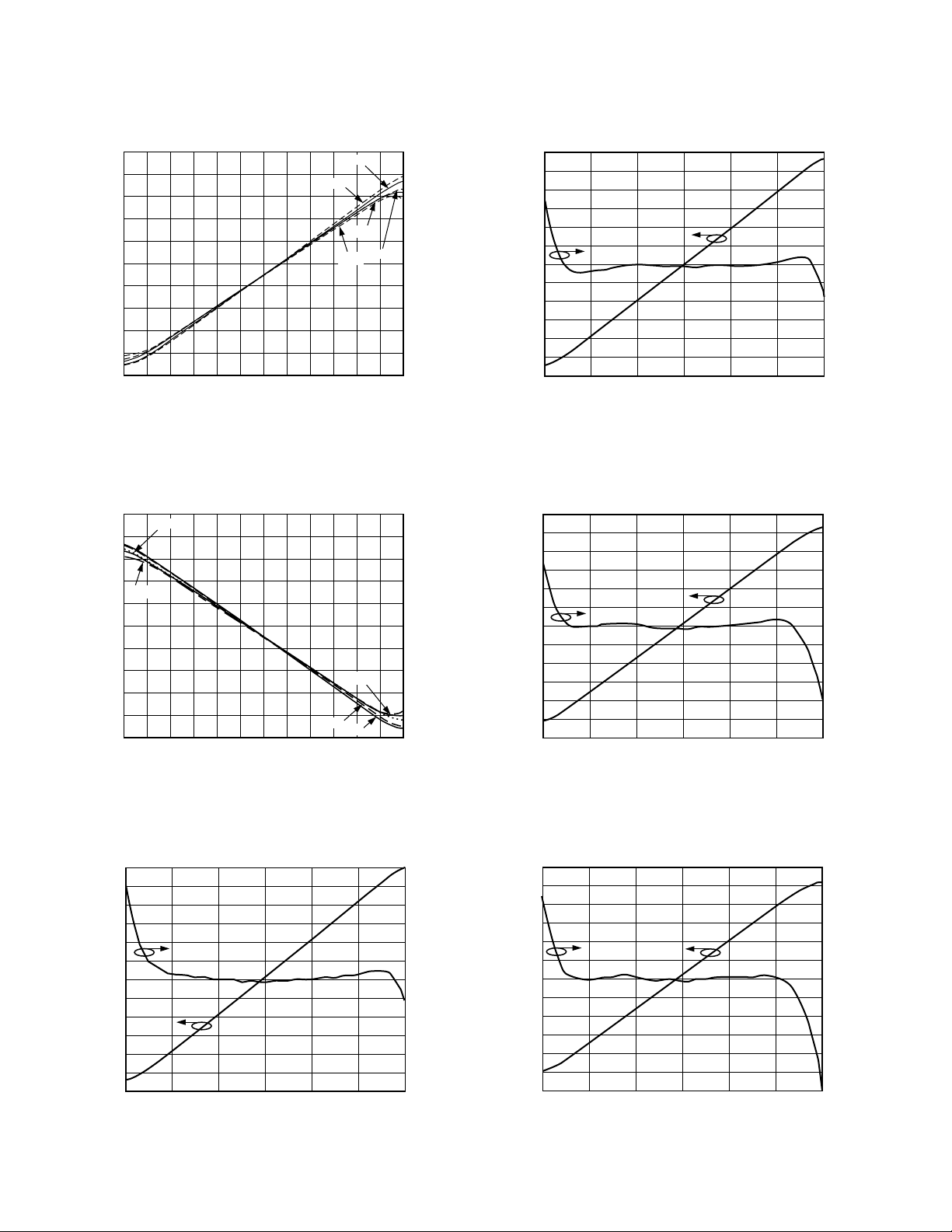
Difference, Input Levels –30 dBm, Frequency 100 MHz
1.80
1.62
1.44
1.26
1.08
0.90
0.72
PHASE OUT – V
0.54
0.36
0.18
1.11022e–16
–180 –150
–120 –90 –60 –300 306090
PHASE DIFFERENCE – Degrees
120 150 180
10
8
6
4
2
0
–2
–4
–6
–8
–10
TPC 28. VPHS Output and Nonlinearity vs. Input Phase
Difference, Input Levels –30 dBm, Frequency 1900 MHz
1.80
1.62
1.44
1.26
1.08
0.90
0.72
PHASE OUT – V
0.54
0.36
0.18
1.11022e–16
–180 –150
–120 –90 –60 –300 306090
PHASE DIFFERENCE – Degrees
120 150 180
10
8
6
4
2
0
–2
–4
–6
–8
–10
TPC 29. VPHS Output and Nonlinearity vs. Input Phase
Difference, Input Levels –30 dBm, Frequency 2200 MHz
ERROR – Degrees
ERROR – Degrees
1.80
1.62
1.44
1.26
1.08
0.90
0.72
PHASE OUT – V
0.54
0.36
0.18
0.00
–180 –150
–120 –90 –60 –300 306090
PHASE DIFFERENCE – Degrees
120 150 180
10
8
6
4
2
0
–2
–4
–6
–8
–10
TPC 27. VPHS Output and Nonlinearity vs. Input Phase
Difference, Input Levels –30 dBm, Frequency 900 MHz
ERROR – Degrees
–10–
8
6
4
2
0
–2
ERROR – Degrees
–4
–6
–8
–10
–180 –15010–120 –90 –60 –300 306090
+25ⴗC
+85ⴗC
–40ⴗC
PHASE DIFFERENCE – Degrees
120 150 180
TPC 30. Distribution of VPHS Error vs. Input Phase Difference, Three Sigma to Either Side of Mean, Frequency
900 MHz, –40°C, +25°C, and +85°C, Input Levels –30 dBm
REV. 0
Page 11

8
TEMPERATURE – ⴗC
CHANGE IN VPHS SLOPE – mV
–40 –30 –20 –100 1020304050
–0.35
60 80 90
MEAN +3 SIGMA
MEAN –3 SIGMA
70
–0.30
–0.25
–0.20
–0.15
–0.10
–0.05
0.00
0.05
0.10
0.15
TEMPERATURE – ⴗC
CHANGE IN PCP – mV
–40 –30 –20 –100 1020304050
–40
60 80 90
+3 SIGMA
–3 SIGMA
70
–35
–30
–25
–20
–15
–10
–5
0
5
10
6
4
2
0
–2
ERROR – Degrees
–4
–6
–8
–10
–180 –15010–120 –90 –60 –300 306090
+25ⴗC
–40ⴗC
+85ⴗC
PHASE DIFFERENCE – Degrees
120 150 180
TPC 31. Distribution of VPHS Error vs. Input Phase Difference, Three Sigma to Either Side of Mean, Frequency
1900 MHz, –40°C, +25°C, and +85°C, Supply 5 V, Input
Levels P
= P
INPA
8
6
4
2
0
–2
ERROR – Degrees
–4
–6
–8
–10
–180 –15010–120 –90 –60 –300 306090
= –30 dBm
INPB
+85ⴗC
+25ⴗC
–40ⴗC
PHASE DIFFERENCE – Degrees
120 150 180
AD8302
TPC 34. Change in VPHS Slope vs. Temperature, Three
Sigma to Either Side of Mean, Frequency 1900 MHz
TPC 32. Distribution of VPHS Error vs. Input Phase Difference, Three Sigma to Either Side of Mean, Frequency
°
2200 MHz, –40
1.8
1.6
1.4
1.2
1.0
0.8
VPHS – V
0.6
0.4
0.2
0.0
–180 –150 –120 –90 –60 –300 306090
TPC 33. Distribution of VPHS vs. Input Phase Difference, Three Sigma to Either Side of Mean, Frequency
900 MHz, Temperature between –40°C and +85°C, Input
Levels –30 dBm
REV. 0
C, +25°C, and +85°C, Input Levels –30 dBm
PHASE DIFFERENCE – Degrees
120 150 180
TPC 35. Change in Phase Center Point (PCP) vs.
Temperature, Three Sigma to Either Side of Mean,
Frequency 1900 MHz
18
15
12
9
PERCENT
6
3
0
0.75 0.80 0.85 0.90 0.95
PCP – V
1.00 1.05
TPC 36. Phase Center Point (PCP) Distribution, Frequency
900 MHz, 17000 units
–11–
Page 12

AD8302
16
14
12
10
8
PERCENT
6
4
2
0
9.5 9.7 9.9 10.1 10.3 10.5 10.7 10.9
VPHS – mV/ Degree
TPC 37. VPHS Slope Distribution, Frequency
900 MHz
10mV PER
VERTICAL
DIVISION
11.1
10mV PER
VERTICAL
DIVISION
50ns HORIZONTAL
TPC 40. VPHS Output Response to 40° Step with Nominal
Phase Shift of 90
, Input Levels P
INPA
= P
= –30 dBm,
INPB
°
Frequency 1900 MHz,1 pF Filter Capacitor
10000
INPUT –50dBm
1000
VPHS – nV/ Hz
100
INPUT –30dBm
INPUT –10dBm
50ns HORIZONTAL
TPC 38. VPHS Output Response to 4° Step with Nominal
°
Phase Shift of 90
1900 MHz, Temperature 25
10mV PER
VERTICAL
DIVISION
, Input Levels –30 dBm Frequency
°
C, 1 pF Filter Capacitor
2s HORIZONTAL
TPC 39. VPHS Output Response to 4° Step with Nominal
°
Phase Shift of 90
, Input Levels P
Supply 5 V, Frequency 1900 MHz, Temperature 25
INPA
= P
= –30 dBm,
INPB
°
C, with
100 pF Filter Capacitor
10
1k
10k 100k 1M 10M 100M
FREQUENCY – Hz
TPC 41. VPHS Output Noise Spectral Density vs. Frequency,
P
= –30 dBm, P
INPA
°
Input Phase Difference
90
1.80
1.62
1.44
1.26
1.08
0.90
0.72
PHASE OUT – V
0.54
0.36
0.18
1.11022e–16
–180 –150
TPC 42. Phase Output vs. Input Phase Difference, P
, P
P
INPB
INPA
= P
INPB
= –10 dBm, –30 dBm, –50 dBm, and
INPB
P
= –30dBm
INPA
= –15dBm
P
INPA
P
= –45dBm
INPA
–120 –90 –60 –300 306090
PHASE DIFFERENCE – Degrees
+15 dB, P
INPA
= P
– 15 dB, Frequency
INPB
120 150 180
INPA
=
900 MHz
–12–
REV. 0
Page 13

AD8302
REAL SHUNT Z (⍀)
FREQUENCY – MHz
RESISTANCE – ⍀
0
4000
500 1000 1500 2000 2500
3500
0
3000
2500
2000
1500
1000
500
CAPACITANCE – pF
4.0
3.5
0.0
3.0
2.5
2.0
1.5
1.0
0.5
SHUNT C
SHUNT R
CAPACITANCE SHUNT Z (pF)
= –15dBm
P
INPA
10
P
= –45dBm
INPA
8
6
4
ABSOLUTE VALUE OF VPHS
INSTANTANEOUS SLOPE – mV
2
0
–180 –15012–120 –90 –60 –300 306090
PHASE DIFFERENCE – Degrees
P
INPA
= –30dBm
120 150 180
TPC 43. Phase Output Instantaneous Slope,
P
INPA
= P
INPB
, P
INPA
= P
+ 15 dB, P
INPB
INPA
= P
– 15 dB,
INPB
Frequency 900 MHz
1.80
1.62
1.44
1.26
1.08
0.90
0.72
PHASE OUT – V
0.54
0.36
0.18
1.11022e–16
–180 –150
P
= –20dBm
INPA
P
= –40dBm
INPA
P
= –30dBm
INPA
–120 –90 –60 –300 306090
PHASE DIFFERENCE – Degrees
120 150 180
TPC 44. Phase Output vs. Input Phase Difference,
P
INPA
= P
INPB
, P
INPA
= P
+ 10 dB, P
INPB
INPA
= P
– 10 dB,
INPB
Frequency 1900 MHz, Supply 5 V
1.80
1.62
1.44
1.26
1.08
0.90
0.72
PHASE OUT – V
0.54
0.36
0.18
1.11022e–16
–180 –150
= –20dBm
P
INPA
P
= –40dBm
INPA
P
= –30dBm
INPA
–120 –90 –60 –300 306090
PHASE DIFFERENCE – Degrees
120 150 180
TPC 46. Phase Output vs. Input Phase Difference,
P
INPA
= P
INPB
, P
INPA
= P
+ 10 dB, P
INPB
INPA
= P
– 10 dB,
INPB
Frequency 2200 MHz
= –20dBm
P
INPA
10
P
P
= –30dBm
8
6
4
ABSOLUTE VALUE OF VPHS
INSTANTANEOUS SLOPE – mV
2
0
–180 –15012–120 –90 –60 –30 0 30 60 90 120 150 180
INPA
PHASE DIFFERENCE – Degrees
TPC 47. Phase Output Instantaneous Slope, P
P
INPA
= P
+ 10 dB, P
INPB
INPA
= P
– 10 dB, Frequency
INPB
INPA
= –40dBm
INPA
2200 MHz
= P
INPB
,
REV. 0
10
P
= –30dBm
INPA
8
P
= –40dBm
6
4
ABSOLUTE VALUE OF VPHS
INSTANTANEOUS SLOPE – mV
2
0
–180 –15012–120 –90 –60 –300 306090
TPC 45. Phase Output Instantaneous Slope, P
, P
P
INPB
Frequency 1900 MHz, Supply 5 V
INPA
INPA
= –20dBm
P
INPA
PHASE DIFFERENCE – Degrees
= P
+ 10 dB, PINPA = P
INPB
120 150 180
– 10 dB,
INPB
INPA
=
TPC 48. Input Impedance, Modeled as Shunt R in Parallel
with Shunt C
–13–
Page 14

AD8302
18
6
4
2
0
VREF – mV
–2
–4
–6
–40 –308–20 –100 10203040506070 90
TEMPERATURE – ⴗC
80
TPC 49. Change in VREF vs. Temperature, Three Sigma to
Either Side of Mean
120
100
80
60
15
12
9
PERCENT
6
3
0
1.74
1.78 1.82 1.84 1.86 1.88
1.76 1.80
VREF – V
TPC 51. VREF Distribution, 17,000 Units
NOISE – nV/ Hz
40
20
0
1k
10k 100k 1M 10M 100M
FREQUENCY – Hz
TPC 50. VREF Output Noise Spectral Density vs.
Frequency
–14–
REV. 0
Page 15

AD8302
MFLT
VMAG
MSET
PSET
VPHS
PFLT
VREF
VIDEO OUTPUT – A
INPA
OFSA
COMM
OFSB
INPB
VPOS
+–+
–
60dB LOG AMPS
(7 DETECTORS)
60dB LOG AMPS
(7 DETECTORS)
VIDEO OUTPUT – B
PHASE
DETECTOR
+
–
BIAS
x3
1.8V
GENERAL DESCRIPTION AND THEORY
The AD8302 measures the magnitude ratio, defined here as
“gain,” and phase difference between two signals. A pair of
matched logarithmic amplifiers provide the measurement, their
hard-limited outputs drive the phase detector.
Basic Theory
Logarithmic amplifiers (log amps) provide a logarithmic compression function that converts a large range of input signal
levels to a compact decibel-scaled output. The general mathematical form is
V
= V
OUT
where V
and V
SLP
that log(x) represents the log10(x) function. V
log (VIN/VZ) (1)
SLP
is the input voltage, VZ is called the intercept (voltage)
IN
is called the slope (voltage). It is assumed throughout
is thus the
SLP
“volts/decade,” and since a decade of voltage corresponds to
20 dB, V
/20 is the “volts/dB.” VZ is the value of input
SLP
signal that results in an output of zero and need not correspond
to a physically realizable part of the log amp signal range.
While the slope is fundamentally a characteristic of the log amp,
the intercept is a function of the input waveform as well.
1
Furthermore, the intercept is typically more sensitive to temperature and frequency than the slope. When single log amps
are used for power measurement, this variability introduces
errors into the absolute accuracy of the measurement since the
intercept represents a reference level.
The AD8302 takes the difference in the output of two identical
log amps, each driven by signals of similar waveforms but at
different levels. Since subtraction in the logarithmic domain
corresponds to a ratio in the linear domain, the resulting
output becomes,
V
= V
where V
MAG
INA
SLP
and V
log (V
INA/VINB
are the input voltages, V
INB
) (2)
is the output
MAG
corresponding to the magnitude of the signal level difference
and V
is the slope. Note that the intercept, VZ, has dropped
SLP
out. Unlike the measurement of power, when measuring a dimension less quantity such as relative signal level, no independent
reference or intercept need be invoked. In essence, one signal
serves as the intercept for the other. Variations in intercept due
to frequency, process, temperature, and supply voltage affect both
channels identically and hence do not affect the difference. This
technique depends on the two log amps being well matched
in slope and intercept to ensure cancellation. This is the case
for an integrated pair of log amps. Note that if the two signals
have different waveforms (e.g., different peak-to-average ratios)
or different frequencies, an intercept difference may appear, introducing a systematic offset.
The log amp structure consists of a cascade of linear/limiting
gain stages with demodulating detectors. Further details about
the structure and function of log amps can be found in data
sheets for other log amps produced by Analog Devices
output of the final stage of a log amp is a fully limited signal
over most of the input dynamic range. The limited outputs from
2
. The
both log amps drive an exclusive-OR style digital phase detector.
Operating strictly on the relative zero-crossings of the limited signals, the extracted phase difference is independent of the original
input signal levels. The phase output has the general form,
NOTES
1
See data sheet for the AD640 for a description of the effect of waveform on the
intercept of log amps.
2
For example, see the data sheet for the AD8307.
REV. 0
V
PHS
where V
= VΦ [Φ (V
is the phase slope in mV/degree and Φ is each signal’s
Φ
) – Φ (V
INA
)] (3)
INB
relative phase in degrees.
Structure
The general form of the AD8302 is shown in Figure 2. The
major blocks consist of two demodulating log amps, a phase
detector, output amplifiers, a biasing cell and an output reference voltage buffer. The log amps and phase detector process
the high-frequency signals and deliver the gain and phase information in current form to the output amplifiers. The output
amplifiers determine the final gain and phase scaling. External
filter capacitors set the averaging time constants for the respective outputs. The reference buffer provides a 1.80 V reference
voltage that tracks the internal scaling constants.
Figure 2. General Structure of the AD8302
Each log amp consists of a cascade of six 10 dB gain stages with
seven associated detectors. The individual gain stages have 3 dB
bandwidths in excess of 5 GHz. The signal path is fully differential to minimize the effect of common-mode signals and noise.
Since there is a total of 60 dB of cascaded gain, slight dc offsets
can cause limiting of the latter stages, which may cause measurement errors for small signals.
The nominal high-pass corner frequency, fHP, of this loop
loop.
This is corrected by a feedback
is set internally at 200 MHz but can be lowered by adding external
capacitance to the OFSA and OFSB pins. Signals at frequencies
well below the high-pass corner are indistinguishable
from dc
offsets and are also nulled. The difference in the log amp outputs is performed in the current domain yielding, by analogy to
Equation 2,
I
= I
LA
where I
and I
LA
SLP
log (V
INA/VINB
are the output current difference and the
SLP
) (4)
characteristic slope (current) of the log amps, respectively. The
slope is derived from an accurate reference designed to be insensitive to temperature and supply voltage.
The phase detector uses a fully symmetric structure with respect
to its two inputs in order to maintain balanced delays along both
signal paths. Fully differential signaling again minimizes the
sensitivity to common-mode perturbations. The current-mode
equivalent to Equation 3 is,
I
where I
= IΦ [Φ (V
PD
and IΦ are the output current and characteristic slope
PD
) – Φ (V
INA
) –90°] (5)
INB
associated with the phase detector, respectively. The slope is
derived from the same reference as the log amp slope.
–15–
Page 16

AD8302
Note that by convention, the phase difference is taken in the range
from –180° to +180°. Since this style of phase detector does not
distinguish between ±90° it is considered to have an unambiguous
180° phase difference range which can be either 0° to +180° centered at 90°, or 0° to –180° centered at –90°.
The basic structure of both output interfaces is shown in Figure 3. It
accepts a setpoint input and includes an internal integrating/averaging capacitor and a buffer amplifier with gain K. External access to
these setpoints provides for several modes of operation and enables
flexible tailoring of the gain and phase transfer characteristics. The
setpoint interface block, characterized by a transresistance RF, generates a current proportional the voltage presented to its input pin,
MSET or PSET. A precise offset voltage of 900 mV is introduced
internally to establish the center-point (V
) for the gain and phase
CP
functions; i.e., the setpoint voltage that corresponds to a gain of 0 dB
and a phase difference of 90°. This setpoint current is subtracted
from the signal current, I
, coming from the log amps in the gain
IN
channel or from the phase detector in the phase channel. The resulting difference is integrated on the averaging capacitors at either pin
MFLT or PFLT and then buffered by the output amplifier to the
respective output pins, VMAG and VPHS. With this open-loop
arrangement, the output voltage is a simple integration of the difference between the measured gain/phase and the desired setpoint,
V
= RF (IIN–IFB )/(sT), (6)
OUT
where I
setpoint input and T is integration time constant equal to R
where C
external capacitor C
I
IN
is the feedback current equal to (V
FB
is the parallel combination of the internal 1.5 pF and the
= I
LA OR IPD
AVE
I
FB
.
FLT
1.5pF
+
–
)/RF ,V
SET–VCP
MFLT/PFLT
K
V
= 900mV
CP
R
+
F
+
VMAG/VPHS
MSET/PSET
20k⍀
is the
SET
FCAVE
/K,
C
FLT
Figure 3. Simplified Block Diagram of the Output Interface
VP
C7
R4
V
INA
V
INB
C1
R1
C4
C6
R2
C5
C3
AD8302
COMM MFLT
1
INPA VMAG
213
312
OFSA MSET
411
VPOS VREF
510
OFSB PSET
69
INPB VPHS
78
COMM PFLT
14
V
MAG
C2
V
PHS
C8
Figure 4. Basic Connections for the AD8302 in Measurement
Mode with 30 mV/dB and 10 mV/Degree Scaling
In the low frequency limit, the gain and phase transfer functions
given in Equations 4 and 5 become,
V
= RFI
MAG
V
= (RFI
MAG
V
= –RFIΦ (|Φ (V
PHS
which are illustrated in Figure 5. In Equation 8b, P
the power in dBm equivalent to V
SLP
SLP
log (V
/20) (P
INA/VINB
INA–PINB
) – Φ (V
INA
)+ VCP or (8a)
INA
)+V
INB
and V
CP
)|–90°) + V
INB
CP
INA
at a specified refer-
and P
INB
(8b)
are
(9)
ence impedance. For the gain function, the slope represented by
is 600 mV/decade or dividing by 20 dB/decade, 30 mV/dB.
R
FISLP
With a center-point of 900 mV for 0 dB gain, a range of –30 dB to
+30 dB covers the full-scale swing from 0 V to 1.8 V. For the phase
function, the slope represented by R
is 10 mV/degree. With a
FIΦ
center-point of 900 mV for 90°, a range of 0° to +180° covers the
full-scale swing from 1.8 V to 0 V. The range of 0° to –180° covers
the same full-scale swing but with the opposite slope.
1.8V
30 mV/dB
MAG
900mV
V
V
CP
BASIC CONNECTIONS
Measurement Mode
The basic function of the AD8302 is the direct measurement of gain
and phase. When the output pins, VMAG and VPHS, are connected
directly to the feedback setpoint input pins, MSET and PSET, the
default slopes and center-points are invoked. This basic connection
shown in Figure 4 is termed the measurement mode. The current
from the setpoint interface is forced by the integrator to be equal to
the signal currents coming from the log amps and phase detector.
The closed loop transfer function is thus given by
V
= (IIN RF +VCP)/(1+ sT). (7)
OUT
The time constant T represents the single-pole response to the envelope of the dB-scaled gain and the degree-scaled phase functions. A
small internal capacitor sets the maximum envelope bandwidth to
approximately 30 MHz. If no external C
is used, the AD8302
FLT
can follow the gain and phase envelopes within this bandwidth. If
longer averaging is desired, C
ing to T (ns) = 3.3 × C
AVE
can be added as necessary accord-
FLT
(pF). For best transient response with
minimal overshoot, it is recommended that 1 pF minimum value
external capacitors be added to the MFLT and PFLT pins.
–16–
0V
–30 0 +30
1.8V
+10 mV/DEG –10 mV/DEG
PHS
V
900mV
0V
–180 –90 0 90 180
MAGNITUDE RATIO – dB
PHASE DIFFERENCE – Degrees
V
CP
Figure 5. Idealized Transfer Characteristics for the Gain
and Phase Measurement Mode
REV. 0
Page 17

AD8302
Interfacing to the Input Channels
The single-ended input interfaces for both channels are identical
and each consists of a driving pin, INPA and INPB, and an ac
grounding pin, OFSA and OFSB. All four pins are internally dc
biased at about 100 mV from the positive supply and should be
externally ac-coupled to the input signals and to ground. For the
signal pins, the coupling capacitor should offer negligible impedance at the signal frequency. For the grounding pins, the coupling
capacitor has two functions: it provides ac grounding and sets the
high-pass corner frequency for the internal offset compensation
loop. There is an internal 10 pF capacitor to ground that sets the
maximum corner to approximately 200 MHz. The corner can be
lowered according the formula f
(MHz) = 2/CC(nF), where C
HP
C
is the total capacitance from OFSA or OFSB to ground, including
the internal 10 pF.
The input impedance to INPA and INPB is a function of
frequency, the offset compensation capacitor and package
parasitics. At moderate frequencies above f
, the input network
HP
can be approximated by a shunt 3 kΩ resistor in parallel with a
2 pF capacitor. At higher frequencies, the shunt resistance
decreases to approximately 500 Ω. The Smith chart in Figure 6
shows the input impedance over the frequency range 100 MHz
to 3 GHz.
Dynamic Range
The maximum measurement range for the gain subsystem is
limited to a total of 60 dB distributed from –30 dB to +30 dB.
This means that both gain and attenuation can be measured.
The limits are determined by the minimum and maximum levels
that each individual log amp can detect. In the AD8302, each log
amp can detect inputs ranging from –73 dBV (223 µV, –60 dBm
re: 50 Ω to –13 dBV (223 mV, 0 dBm re: 50 Ω). Note that log
amps respond to voltages and not power. An equivalent power
can be inferred given an impedance level, e.g., to convert from
dBV to dBm in a 50 Ω system, simply add 13 dB. To cover the
entire range, it is necessary to apply a reference level to one log
amp that corresponds precisely to its midrange. In the AD8302,
this level is at –43 dBV, which corresponds to –30 dBm in a
50 Ω environment. The other channel can now sweep from its
low end, 30 dB below midrange, to its high end, 30 dB above
midrange. If the reference is displaced from midrange, some
measurement range will be lost at the extremes. This can occur
either if the log amps run out of range or if the rails at ground or
1.8 V are reached. Figure 7 illustrates the effect of the reference
channel level placement. If the reference is chosen lower than
midrange by 10 dB, then the lower limit will be at –20 dB rather
than –30 dB. If the reference chosen is higher by 10 dB, the upper
limit will be 20 dB rather than 30 dB.
= V
REF
OPT
1.80
MAX RANGE FOR V
REF
100MHz
900MHz
1.8GHz
2.7GHz
3.0GHz
2.2GHz
Figure 6. Smith Chart Showing the Input Impedance of a
Single Channel from 100 MHz to 3 GHz
A broadband resistive termination on the signal side of the
coupling capacitors can be used to match to a given source
impedance. The value of the termination resistor, R
, is deter-
T
mined by,
RT = RIN RS/(R
where R
IN
is the input resistance and RS the source impedance.
– RS) (10)
IN
At higher frequencies, a reactive, narrow-band match might be
desirable to tune out the reactive portion of the input impedance. An important attribute of the two-log-amp architecture is
that if both channels are at the same frequency and have the same
input network, then impedance mismatches and reflection losses
become essentially common-mode and hence do not impact the
relative gain and phase measurement. However, mismatches in
these external components can result in measurement errors.
0.90
VMAG – V
V
REF
–30 0 +30
OPT
< V
REF
GAIN MEASUREMENT RANGE – dB
V
REF
> V
REF
OPT
Figure 7. The Effect of Offsetting the Reference Level is to
Reduce the Maximum Dynamic Range.
The phase measurement range is of 0 to 180°. For phase differ-
ences of 0° to –180°, the transfer characteristics are mirrored as
shown in Figure 5, with a slope of the opposite sign. The phase
detector responds to the relative position of the zero crossings
between the two input channels. At higher frequencies, the finite
rise and fall times of the amplitude limited inputs create an
ambiguous situation that leads to inaccessible dead zones at the
0° and 180° limits. For maximum phase difference coverage, the
reference phase difference should be set to 90°.
REV. 0
–17–
Page 18

AD8302
Cross-modulation of Magnitude and Phase
At high frequencies, unintentional cross coupling between signals
in channels A and B inevitably occurs due to on-chip and boardlevel parasitics. When the two signals presented to the AD8302
inputs are at very different levels, the cross-coupling introduces
cross-modulation of the phase and magnitude responses. If the two
signals are held at the same relative levels and the phase between
them is modulated, then only the phase output should respond.
Due to phase-to-amplitude cross modulation, the magnitude output shows a residual response. A similar effect occurs when the
relative phase is held constant while the magnitude difference is
modulated; i.e an expected magnitude response and a residual
phase response are observed due to amplitude-to-phase cross
modulation. The point where these effects are noticeable depends
on the signal frequency and the magnitude of the difference. Typically, for differences <20 dB, the effects of cross modulation are
negligible at 900 MHz.
Modifying the Slope and Center-Point
The default slope and center-point values can be modified with
the addition of external resistors. Since the output interface
blocks are generalized for both magnitude and phase functions,
the scaling modification techniques are equally valid for both
outputs. Figure 8 demonstrates how a simple voltage divider
from the VMAG and VPHS pins to the MSET and PSET pins
can be used to modify the slope. The increase in slope is given
by 1 + R1/(R2储20 kΩ). Note that it may be necessary to account
for the MSET and PSET input impedance of 20 kΩ which has a
±20% manufacturing tolerance. As is generally true in such feedback systems, envelope bandwidth is decreased and the output
noise transferred from the input is increased by the same factor.
For example, by selecting R1 and R2 to be 10 kΩ and 20 kΩ,
respectively, gain slope increases from the nominal 30 mV/dB by
a factor of 2 to 60 mV/dB. The range is reduced by a factor of
two and the new center-point is at –15 dB; i.e. the range now
extends from –30 dB, corresponding to V
corresponding to V
= 1.8 V.
MAG
= 0 V, to 0 dB,
MAG
bandgap reference that determines the nominal center-point,
their tracking with temperature, supply and part-to-part variations should be better in comparison to a fixed external voltage.
If the center-point is shifted to 0 dB in the previous example
where the slope was doubled, then the range spans from –15 dB
at V
= 0 V to 15 dB at V
MAG
VMAG
MSET
20k⍀
VREF
= 1.8 V.
MAG
NEW SLOPE = 30mV/dB ⴛ
R1
20k⍀
1ⴙ
R1
10k⍀
Figure 9. The Center-Point is Repositioned with the Help
of the Internal Reference Voltage of 1.80 V
Comparator and Controller Modes
The AD8302 can also operate in a comparator mode if used in
the arrangement shown in Figure 10 where the DUT is the element to be evaluated. The VMAG and VPHS pins are no longer
connected to MSET and PSET. The trip-point thresholds for
the gain and phase difference comparison are determined by the
voltages applied to pins MSET and PSET according to,
V
(V ) = 30 mV/dB × GainSP (dB) + 900 mV (11)
MSET
V
(V )= –10 mV/° × (|PhaseSP (°)|–90°) + 900 mV (12)
PSET
where Gain
SP
(dB) and PhaseSP (°) are the desired gain and
phase thresholds. If the actual gain and phase between the two
input channels differ from these thresholds, the V
MAG
and V
PHS
outputs toggle like comparators; i.e.,
= (13)
V
MAG
0 V if Gain < Gain
1.8 V if Phase > Phase
= (14)
V
PHS
1.8 V if Gain > Gain
0 V if Phase < Phase
SP
SP
SP
SP
VMAG
20k⍀
MSET
NEW SLOPE = 30mV/dB ⴛ
R1
R2
1ⴙ
||R20k⍀
R2
R1
Figure 8. Increasing the Slope Requires the Inclusion of a
Voltage Divider
Repositioning the center-point back to its original value of 0 dB
simply requires that an appropriate voltage be applied to the
grounded side of the lower resistor in the voltage divider. This
voltage may be provided externally or derived from the internal reference voltage on pin VREF. For the specific choice of
R2 = 20 kΩ, the center-point is easily readjusted to 0 dB by connecting the VREF pin directly to the lower pin of R2 as shown in
Figure 9. The increase in slope is now simplified to 1 + R1/10 kΩ.
Since this 1.80 V reference voltage is derived from the same
–18–
VP
C7
V
INA
R1
R2
V
INB
R4
C1
C4
C6
C5
C3
AD8302
COMM MFLT
1
INPA VMAG
213
312
OFSA MSET
411
VPOS VREF
510
OFSB PSET
69
INPB VPHS
78
COMM PFLT
14
V
V
V
V
C2
MAG
MSET
PSET
PHS
C8
Figure 10. Disconnecting the Feedback to the Setpoint
Controls, the AD8302 Operates in Comparator Mode
REV. 0
Page 19

AD8302
The comparator mode can be turned into a controller mode by
closing the loop around the V
MAG
and V
outputs. Figure 11
PHS
illustrates a closed loop controller that stabilizes the gain and phase
of a DUT with gain and phase adjustment elements. If V
V
are properly conditioned to drive gain and phase adjustment
PHS
MAG
and
blocks preceding the DUT, the actual gain and phase of the DUT
will be servoed toward the prescribed setpoint gain and phase given
in Equations 11 and 12. These are essentially AGC and APC
loops. Note that as with all control loops of this kind, loop dynamics and appropriate interfaces all must be considered in more detail.
AD8302
VMAG
MSET
PSET
VPHS
MAG
SETPOINT
PHASE
SETPOINT
⌬MAG
⌬⌽
INPA
INPB
Figure 11. By applying overall feedback to a DUT via
external gain and phase adjusters, the AD8302 acts
as a controller.
APPLICATIONS
Measuring Amplifier Gain and Compression
The most fundamental application of AD8302 is the monitoring
of the gain and phase response of a functional circuit block such
as an amplifier or a mixer. As illustrated in Figure 12, directional couplers, DC
and DCA, sample the input and output
B
signals of the “Black Box” DUT. The attenuators ensure that
the signal levels presented to the AD8302 fall within its dynamic
range. From the discussion in the Dynamic Range section, the
optimal choice places both channels at P
= –30 dBm refer-
OPT
enced to 50 Ω, which corresponds to –43 dBV. To achieve this,
the combination of coupling factor and attenuation are given by,
C
+ LB = PIN – P
B
C
+ LA = PIN + GAIN
A
where C
and CA are the coupling coefficients, LB and LA are the
B
OPT
NOM–POPT
attenuation factors and GAIN
is the nominal DUT gain. If
NOM
(15)
(16)
identical couplers are used for both ports, then the difference in
the two attenuators compensates for the nominal DUT gain. When
the actual gain is nominal, the V
output is 900 mV, corresponding
MAG
to 0 dB. Variations from nominal gain appear as a deviation from
900 mV or 0 dB with a 30 mV/dB scaling. Depending on the nominal
insertion phase associated with DUT, the phase measurement may
require a fixed phase shift in series with one of the channels to
bring the nominal phase difference presented to the AD8302
near the optimal 90° point.
When the insertion phase is nominal, the VPHS output is 900 mV.
Deviations from the nominal are reported with a 10 mV/degree
scaling. Table I gives suggested component values for the measurement of an amplifier with a nominal gain of 10 dB and an
input power of –10 dBm.
ATTEN
A
DC
OUTPUTINPUT
“BLACK BOX”
DC
A
B
VP
C7
R4
C1
R1
C4
C6
R2
C5
C3
AD8302
COMM MFLT
1
INPA VMAG
213
312
OFSA MSET
411
VPOS VREF
510
OFSB PSET
69
INPB VPHS
78
COMM PFLT
ATTEN
B
14
C2
R5
R6
C8
H
H
Figure 12. Using the AD8302 to Measure the Gain and
Insertion Phase of an Amplifier or Mixer
Table I. Component Values for Measuring a 10 dB Amplifier
with an Input Power of –10 dBm
Component Value Quantity
R1, R2 52.3 Ω 2
R5, R6 100 Ω 2
C1, C4, C5, C6 0.001 µF4
C2, C8 Open
C3 100 pF 1
C7 0.1 µF1
AttenA 10 dB (See Text) 1
AttenB 1 dB (See Text) 1
DCA, DC
B
20 dB 2
The gain measurement application can also monitor gain and
phase distortion in the form of AM-AM (gain compression) and
AM-PM conversion. In this case, the nominal gain and phase
corresponds to those at low input signal levels. As the input level
is increased, output compression and excess phase shifts are
measured as deviations from the low level case. Note that the signal
levels over which the input is swept must remain within the dynamic
range of the AD8302 for proper operation.
REV. 0
–19–
Page 20

AD8302
Reflectometer
The AD8302 can be configured to measure the magnitude ratio
and phase difference of signals that are incident on and reflected
from a load. The vector reflection coefficient, ⌫ is defined as,
⌫
= Reflected Voltage/Incident Voltage = (ZL – ZO)/(ZL + ZO), (16)
where Z
is the complex load impedance and ZO is the charac-
L
teristic system impedance.
The measured reflection coefficient can be used to calculate the
level of impedance mismatch or standing wave ratio (SWR) of a
particular load condition. This proves particularly useful in diagnosing varying load impedances such as antennas that can degrade
performance and even cause physical damage. The vector
reflectometer arrangement given in Figure 13 consists of a pair
of directional couplers that sample the incident and reflected signals. The attenuators reposition the two signal levels within the
dynamic range of the AD8302. In analogy to Equations 14 and
15, the attenuation factors and coupling coefficients are given by,
C
+ LB = PIN – P
B
C
+ LA = PIN +
A
where
⌫
NOM
OPT
⌫
NOM – POPT
is the nominal reflection coefficient in dB and is
(17)
(18)
negative for passive loads. Consider the case where the incident
signal is 10 dBm and the nominal reflection coefficient is –19 dB.
As shown in Figure 13, using 20 dB couplers on both sides and
–30 dBm for P
, the attenuators for Channel A and B paths are
OPT
1 dB and 20 dB, respectively. The magnitude and phase of the
reflection coefficient are available at the VMAG and VPHS pins
scaled to 30 mV/dB and 10 mV/degree. When ⌫ is –19 dB, the
VMAG output is 900 mV.
The measurement accuracy can be compromised if board
level details are not addressed. Minimize the physical distance
between the series connected couplers since the extra path
length adds phase error to ⌫. Keep the paths from the couplers
to the AD8302 as well matched as possible since any differences
introduce measurement errors. The finite directivity, D, of the
couplers sets the minimum detectable reflection coefficient, i.e.,
(dB)|<|D(dB)|.
|G
MIN
SOURCE
INCIDENT
WAVE
C3
REFLECTED
1dB
20dB
R2
R1
C1C4C6C5
AD8302
COMM MFLT
1
INPA VMAG
213
312
OFSA MSET
411
VPOS VREF
510
OFSB PSET
69
INPB VPHS
78
COMM PFLT
WAVE
R4
C2
14
Z
LOAD
VP
C7
⌫
R5
⌫
R6
C8
–20–
Figure 13. Using the AD8302 to Measure the Vector
Reflection Coefficient Off an Arbitrary Load
REV. 0
Page 21

INPA
GND
INPB
AD8302
VP
VP
C7
R4
AD8302
MFLT
COMM
C1
R1
C4
C6
R2
C5
1
INPA
2
3
OFSA
4
VPOS
5
OFSB
6
INPB
7
C3
COMM
VMAG
MSET
VREF
PSET
VPHS
PFLT
14
C2
13
12
R7
11
SW2
10
R8
9
8
C8
Figure 14. Evaluation Board Schematic
R3
R6
R5
SW1
GAIN
Table II. P1 Pin Allocations
1 Common
VREF
R9
PSET
PHASE
GSET
2 VPOS
3 Common
Figure 15a. Component Side Metal of Evaluation Board
Figure 15b. Component Side Silk Screen of Evaluation Board
Table III. Evaluation Board Configuration Options
Component Function Default Condition
P1 Power Supply and Ground Connector: Pin 2 VPOS, and Pins 1 and 3 Ground. Not Applicable
R1, R2 Input termination: Provide Termination for Input Sources. R1 = R2 = 52.3 Ω (Size 0402)
R3 VREF Output Load: This load is optional and is meant to allow R3 = 1 kΩ (Size 0603)
the user to simulate their circuit loading of the device.
R5, R6, R9 Snubbing Resistor R5 = R6 = 0 Ω (Size 0603)
R9 = 0 Ω (Size 0603)
C3, C7, R4 Supply Decoupling C3 = 100 pF (Size 0603)
C7 = 0.1 µF (Size 0603)
R4 = 0 Ω (Size 0603)
C1, C5 Input AC-Coupling Capacitors C1 = C5 = 1 nF (Size 0603)
C2, C8 Video Filtering: C2 and C8 limit the video bandwidth of the Gain and Phase C2 = C8 = Open (Size 0603)
output respectively.
C4, C6 Offset Feedback: These set the high-pass corner of the offset cancellation loop,
and thus with the input AC-coupling capacitors the minimum operating frequency. C4 = C6 = 1 nF (Size 0603)
SW1 GSET Signal Source: When SW1 is in the position shown, the device is in gain SW1 = Installed
measure mode, when switched it operates in comparator mode and a signal
must be applied to GSET.
SW2 PSET signal source: When SW2 is in the position shown, the device is in phase SW1 = Installed
measure mode, when switched it operates in comparator mode and a signal
must be applied to PSET.
REV. 0
–21–
Page 22

AD8302
CHARACTERIZATION SETUPS AND METHODS
The general hardware configuration used for most of the AD8302
characterization is shown in Figure 16. The characterization board
is similar to the Customer Evaluation Board. Two reference-locked
R & S SMT03 signal generators are used as the inputs to INPA
and INPB, while the Gain and Phase outputs are monitored using
both a TDS 744A oscilloscope with 10× high impedances probes and
Agilent 34401A multimeters.
Gain
The basic technique used to evaluate the static gain (VMAG)
performance was to set one source to a fixed level and sweep the
amplitude of the other source, while measuring the VMAG output
with the DMM. In practice the two sources were run at 100 kHz
frequency offset and average output measured with the DMM to
alleviate errors that might be induced by gain/phase modulation
due to phase jitter between the two sources.
The errors stated are the difference between a best fit line calculated by a linear regression and the actual measured data divided
by the slope of the line to give an error in V/dB. The “referred to
25°C error” uses this same method, while always using the slope
and intercept calculated for that device at 25°C.
Response measurement made of the VMAG output used the
configuration shown in Figure 17. The variable attenuator,
Alpha AD260, is driven with a HP8112A pulse generator producing a change in RF level within 10 ns.
Noise spectral density measurements were made using a
HP3589A with the inputs delivered through a Narda 4032C
90° phase splitter.
To measure the modulation of VMAG due to phase variation
again the sources were run at a frequency offset, f
, effectively
OS
creating a continuous linear change in phase going through 360°
once every 1/f
seconds. The VMAG output is then measured
OS
with a DSO. When perceivable, only at high frequencies and
large input magnitude differences, the linearly ramping phase
creates a near sinusoid output riding on the expected VMAG
DC output level. The curves in TPC 24 show the peak-to-peak
output level measured with averaging.
Phase
The majority of the VPHS output data was collected by generating phase change, again by operating the two input sources with
a small frequency offset (normally 100 kHz) using the same
configuration shown in Figure 16. Although this method gives
excellent linear phase change, good for measurement of slope
and linearity, it lacks an absolute phase reference point. In the
curves showing swept phase the phase at which the VPHS is the
same as VPHS with no input signal is taken to be –90° and all
other angles are references to there. Typical Performance Curves
show two figures of merit; instantaneous slope and error. Instantaneous slope, as shown in TPCs 43, 44, and 45 was calculated
simply by taking the delta in V
over angular change for adjacent
PHS
measurement points.
TEKTRONIX
TDS 744A
OSCILLOSCOPE
MULTIMETER/
OSCILLOSCOPE
HP 34401A
MULTIMETER
SAME SETUP AS
V
MAG
R & S
SIGNAL GENERATOR
SMTO3
R & S
SIGNAL GENERATOR
SMTO3
3dB
3dB
TEKTRONIX
VX1410A
INPA
INPB
EVB
V
MAG
V
REF
V
PHS
Figure 16. Primary Characterization Setup
TEKTRONIX
VX1410A
REF
PHS
TEKTRONIX
P
TDS 744A
OSCILLOSCOPE
R & S
SIGNAL
GENERATOR
SMTO3
SPLITTER
FIXED
ATTEN
VARIABLE
ATTEN
PULSE
GENERATOR
3dB
3dB
INPA
INPB
EVB
V
V
V
MAG
Figure 17. VMAG Dynamic Performance Measurement Setup
–22–
REV. 0
Page 23

OUTLINE DIMENSIONS
Dimensions shown in inches and (mm).
14-Lead Thin Shrink SO Package (TSSOP)
(RU-14)
0.201 (5.10)
0.193 (4.90)
AD8302
PIN 1
0.006 (0.15)
0.002 (0.05)
SEATING
PLANE
14
0.0256
(0.65)
BSC
8
0.177 (4.50)
0.169 (4.30)
71
0.0433 (1.10)
MAX
0.0118 (0.30)
0.0075 (0.19)
0.256 (6.50)
0.246 (6.25)
0.0079 (0.20)
0.0035 (0.090)
8ⴗ
0ⴗ
0.028 (0.70)
0.020 (0.50)
REV. 0
–23–
Page 24

C02492–1–7/01(0)
–24–
PRINTED IN U.S.A.
 Loading...