

Page 1
Low Cost, Zero-Drift In-Amp
V
www.BDTIC.com/ADI
FEATURES
Small package: 8-lead SOT-23
Reduced component count
Incorporates gain resistors and filter resistors
Low offset voltage: 20 μV maximum
Low offset drift: 0.3 μV/°C maximum
Low gain drift: 25 ppm/°C maximum
High CMR: 140 dB typical
Low noise: 0.7 μV p-p from 0.01 Hz to 10 Hz
Single-supply operation: 1.8 V to 5.5 V
Rail-to-rail output
Available in 2 fixed-gain models
APPLICATIONS
Current sensing
Strain gauges
Laser diode control loops
Portable medical instruments
Thermocouple amplifiers
with Filter and Fixed Gain
AD8293G80/AD8293G160
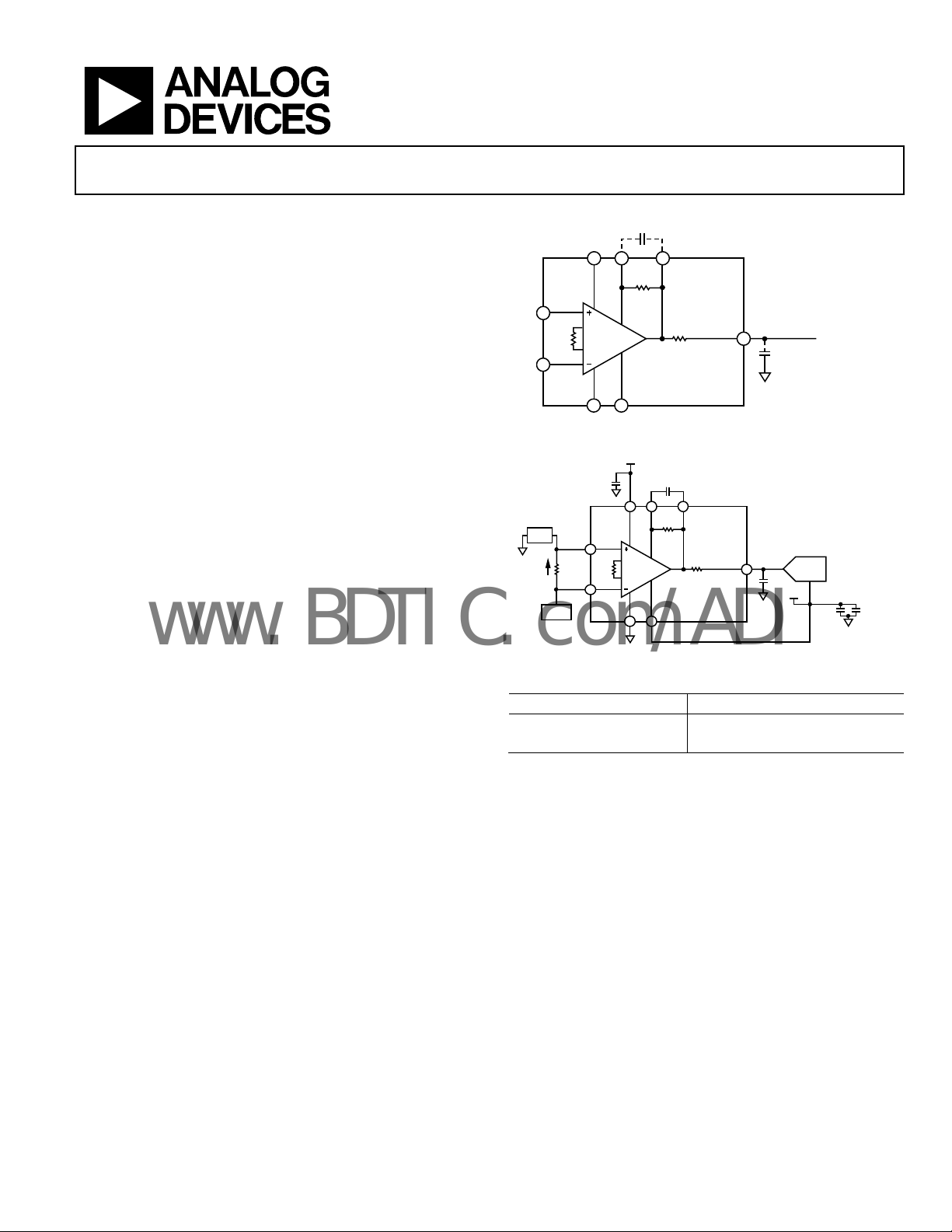
FUNCTIONAL BLOCK DIAGRAM
7 5 6
FILT+V
+5
7 5
S
IN-AMP
R2
REFGND
OUT
R3
5kΩ
ADC OUT
AD8293Gxx
Figure 1.
C2
6
FILT+V
OUT
R2
R3
5kΩ
AD8293Gxx
32
ADC OUT
4
OUTPUT TO ADC
WITH ANTI ALIASING
FILTER
4
C3
+3.3V
ADC
REF
S
+IN
8
R1
IN-AMP
4kΩ
–IN
1
REFGND
32
0.1µF
LOAD
I
1.8V
DC-DC
R
SHUNT
+IN
8
R1
4kΩ
–IN
1
Figure 2. Measuring Current Using the AD8293G80/AD8293G160
07451-001
10µF0.1µF
07451-002
GENERAL DESCRIPTION
The AD8293G80/AD8293G160 are small, low cost, precision
instrumentation amplifiers that have low noise and rail-to-rail
outputs. They are available in two fixed-gain models: 80 and 160.
They incorporate the gain setting resistors and filter resistors,
reducing the number of ancillary components. For example,
only two external capacitors are needed to implement a 2-pole
filter. The AD8293G80/AD8293G160 also feature low offset
voltage, offset drift, and gain drift coupled with high commonmode rejection. They are capable of operating on a supply of
1.8 V to 5.5 V.
With a low offset voltage of 20 µV (AD8293G160B), an offset
voltage drift of 0.3 µV/°C, and a voltage noise of only 0.7 µV p-p
(0.01 Hz to 10 Hz), the AD8293G80/AD8293G160 are ideal
for applications where error sources cannot be tolerated.
Rev. 0
Information furnished by Analog Devices is believed to be accurate and reliable. However, no
responsibility is assumed by Analog Devices for its use, nor for any infringements of patents or other
rights of third parties that may result from its use. Specifications subject to change without notice. No
license is granted by implication or otherwise under any patent or patent rights of Analog Devices.
Trademarks and registered trademarks are the property of their respective owners.
Table 1. AD8293Gxx Models and Gains
Model Gain
AD8293G80 80
AD8293G160 160
Precision instrumentation, position and pressure sensors,
medical instrumentation, and strain gauge amplifiers benefit
from the low noise, low input bias current, and high commonmode rejection. The small footprint and low cost are ideal for
high volume applications.
The small package and low power consumption allow the maximum channel density and the minimum board size required for
portable systems. Designed for ease of use, these instrumentation
amplifiers, unlike more traditional ones, have a buffered reference,
eliminating the need for an additional op amp to set the reference
voltage to midsupply.
The AD8293G80/AD8293G160 are specified over the industrial
temperature range from −40°C to +85°C. The AD8293G80/
AD8293G160 are available in a halogen-free, Pb-free, 8-lead SOT-23.
One Technology Way, P.O. Box 9106, Norwood, MA 02062-9106, U.S.A.
Tel: 781.329.4700 www.analog.com
Fax: 781.461.3113 ©2008 Analog Devices, Inc. All rights reserved.
Page 2

AD8293G80/AD8293G160
www.BDTIC.com/ADI
TABLE OF CONTENTS
Features .............................................................................................. 1
Applications ....................................................................................... 1
Functional Block Diagram .............................................................. 1
General Description ......................................................................... 1
Revision History ............................................................................... 2
Specifications ..................................................................................... 3
Electrical Characteristics ............................................................. 3
Absolute Maximum Ratings ............................................................ 5
Thermal Resistance ...................................................................... 5
ESD Caution .................................................................................. 5
Pin Configuration and Function Descriptions ............................. 6
Typical Performance Characteristics ............................................. 7
REVISION HISTORY
8/08—Revision 0: Initial Version
Theory of Operation ...................................................................... 10
High PSR and CMR ................................................................... 10
1/f Noise Correction .................................................................. 10
Applications Information .............................................................. 11
Overview ..................................................................................... 11
Reference Connection ............................................................... 11
Output Filtering .......................................................................... 11
Clock Feedthrough ..................................................................... 12
Power Supply Bypassing ............................................................ 12
Input Overvoltage Protection ................................................... 12
Outline Dimensions ....................................................................... 13
Ordering Guide .......................................................................... 13
Rev. 0 | Page 2 of 16
Page 3
AD8293G80/AD8293G160
www.BDTIC.com/ADI
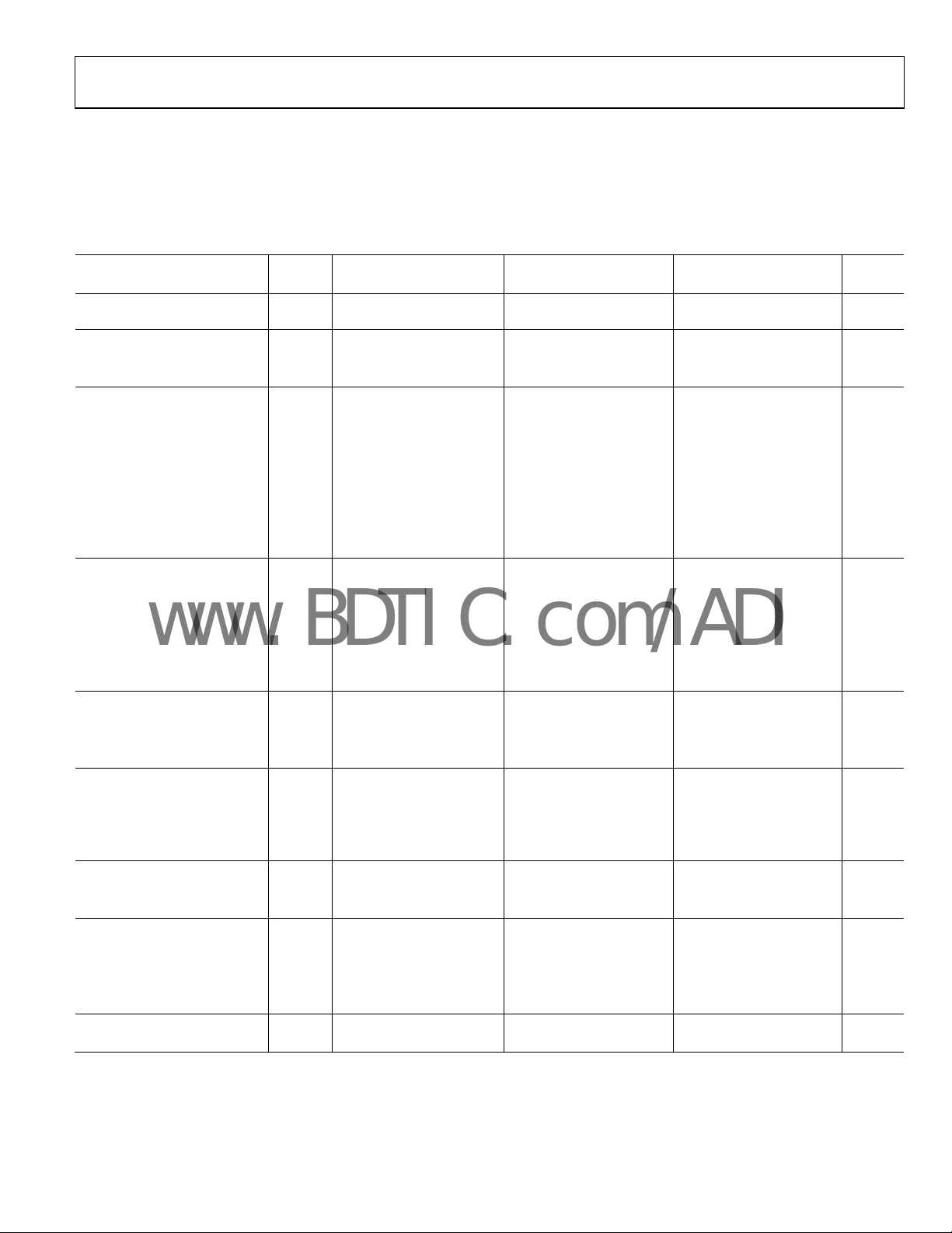
SPECIFICATIONS
ELECTRICAL CHARACTERISTICS
VCC = 5.0 V, VCM = −0 V, V
specifications guaranteed by characterization.
Table 2. A Grade
AD8293G80A AD8293G160A
Parameter Symbol Conditions Min Typ Max Min Typ Max Unit
COMMON-MODE REJECTION CMR
NOISE PERFORMANCE
Voltage Noise e
Voltage Noise Density en f = 1 kHz 35 35 nV/√Hz
INPUT CHARACTERISTICS
Input Offset Voltage VOS 9 50 9 50 μV
vs. Temperature ΔVOS/ΔT −40°C ≤ TA ≤ +85°C 0.02 0.3 0.02 0.3 μV/°C
Input Bias Current IB −40°C ≤ TA ≤ +85°C 0.4 2 0.4 2 nA
Input Offset Current IOS 4 4 nA
Input Operating Impedance
Differential 50||1 50||1 MΩ||pF
Common Mode 10||10 10||10 GΩ||pF
Input Voltage Range 0 VCC − 1.7 0 VCC − 1.7 V
DYNAMIC RESPONSE
Small Signal Bandwidth
Slew Rate SR Filter limited Filter limited
Settling Time
2
t
0.1% 500 Hz filter, VO = 2 V step 1.9 1.9 ms
0.01% 2.4 2.4 ms
Internal Clock Frequency 60 60 kHz
GAIN 80 160
Gain Error VO = 0.075 V to 4.925 V 0.3 1 0.3 1 %
Gain Drift −40°C ≤ TA ≤ +85°C 5 25 5 25 ppm/°C
Nonlinearity VO = 0.075 V to 4.925 V 0.003 0.03 0.003 0.03 % FS
OUTPUT CHARACTERISTICS
Output Voltage High VOH
Output Voltage Low VOL 0.075 0.075 V
Short-Circuit Current ISC ±35 ±35 mA
REFERENCE CHARACTERISTICS
V
Range 0.8 VCC − 0.8 0.8 VCC − 0.8 V
REF
REF Pin Current I
POWER SUPPLY
Operating Range 1.8 5.5 1.8 5.5 V
Power Supply Rejection PSR VCC = 1.8 V to 5.5 V, VCM = 0 V 94 120 94 120 dB
Supply Current ISY I
−40°C ≤ TA ≤ +85°C 1.5 1.5 mA
TEMPERATURE RANGE
Specified Range −40 +85 −40 +85 °C
1
Higher bandwidths result in higher noise.
2
Settling time is determined by filter setting.
= 3.3 V, VIN = V
REF
f = 0.01 Hz to 10 Hz 0.7 0.7 μV p-p
n p-p
1
BW Filter limited 500 500 Hz
s
0.01 1 0.01 1 nA
REF
− V
INP
V
CM
−40°C ≤ T
= 0 mA, VIN = 0 V 1.0 1.3 1.0 1.3 mA
O
, TA = 25°C, tested at ADC OUT, unless otherwise noted. Temperature
INN
= 0 V to 3.3 V,
≤ +85°C
A
Rev. 0 | Page 3 of 16
94 140 94 140 dB
−
V
CC
0.075
−
V
CC
0.075
V
Page 4
AD8293G80/AD8293G160
www.BDTIC.com/ADI
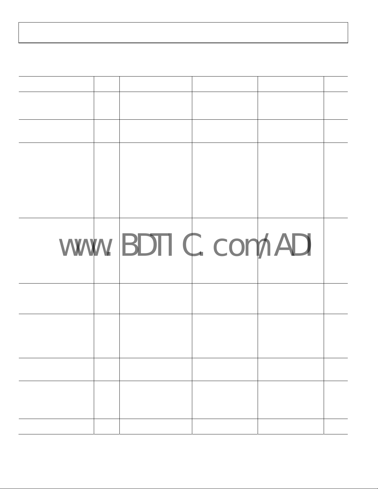
VCC = 2.7 V to 5.0 V, VCM = −0 V, V
otherwise noted. Temperature specifications guaranteed by characterization.
Table 3. B Grade (Tested and Guaranteed over a Wider Supply Range to More Stringent Specifications Than the A Grade)
AD8293G80B AD8293G160B
Parameter Symbol Conditions Min Typ Max Min Typ Max Unit
COMMON-MODE REJECTION CMR
NOISE PERFORMANCE
Voltage Noise e
Voltage Noise Density en f = 1 kHz 35 35 nV/√Hz
INPUT CHARACTERISTICS
Input Offset Voltage VOS 5 30 3 20 μV
vs. Temperature ΔVOS/ΔT −40°C ≤ TA ≤ +85°C, VCC = 5 V 0.02 0.3 0.02 0.3 μV/°C
vs. Temperature ΔVOS/ΔT −40°C ≤ TA ≤ +85°C, VCC = 2.7 V 0.01 0.5 0.01 0.5 μV/°C
Input Bias Current IB −40°C ≤ TA ≤ +85°C 0.4 2 0.4 2 nA
Input Offset Current IOS 4 4 nA
Input Operating Impedance
Differential 50||1 50||1 MΩ||pF
Common Mode 10||10 10||10 GΩ||pF
Input Voltage Range 0 VCC − 1.7 0 VCC − 1.7 V
DYNAMIC RESPONSE
Small Signal Bandwidth
1
BW
Slew Rate SR Filter limited Filter limited
Settling Time
2
t
0.1%
0.01% 2.4 2.4 ms
Internal Clock Frequency 60 60 kHz
GAIN 80 160
Gain Error VO = 0.075 V to 4.925 V 0.3 0.5 0.3 0.5 %
Gain Drift −40°C ≤ TA ≤ +85°C 5 25 5 25 ppm/°C
Nonlinearity VO = 0.075 V to 4.925 V 0.003 0.009 0.003 0.009 % FS
OUTPUT CHARACTERISTICS
Output Voltage High VOH
Output Voltage Low VOL 0.075 0.075 V
Short-Circuit Current ISC V
V
REFERENCE CHARACTERISTICS
V
Range 0.8 VCC − 0.8 0.8 VCC − 0.8 V
REF
REF Pin Current I
POWER SUPPLY
Operating Range 1.8 5.5 1.8 5.5 V
Power Supply Rejection PSR VCC = 1.8 V to 5.5 V, VCM = 0 V 100 120 100 120 dB
Supply Current ISY I
−40°C ≤ TA ≤ +85°C 1.5 1.5 mA
TEMPERATURE RANGE
Specified Range −40 +85 −40 +85 °C
1
Higher bandwidths result in higher noise.
2
Settling time is determined by filter setting.
= VCC/2, VIN = V
REF
= 5 V, VCM = 0 V to 3.3 V;
V
CC
−40°C ≤ T
= 2.7 V, VCM = 0 V to 1 V;
V
CC
−40°C ≤ T
f = 0.01 Hz to 10 Hz 0.7 0.7 μV p-p
n p-p
Filter limited; measured at
− V
INP
≤ +85°C
A
≤ +85°C
A
, TA = 25°C, tested at OUT with 10 kΩ load and ADC OUT, unless
INN
110 140 110 140 dB
106 140 106 140 dB
500 500 Hz
ADC OUT
s
500 Hz filter, V
= 2 V step;
O
1.9 1.9 ms
measured at ADC OUT
V
CC
0.075
= 5 V ±35 ±35 mA
CC
= 2.7 V ±25 ±25 mA
CC
0.01 1 0.01 1 nA
REF
= 0 mA, VIN = 0 V 1.0 1.3 1.0 1.3 mA
O
Rev. 0 | Page 4 of 16
V
0.075
−
V
−
CC
Page 5
AD8293G80/AD8293G160
www.BDTIC.com/ADI
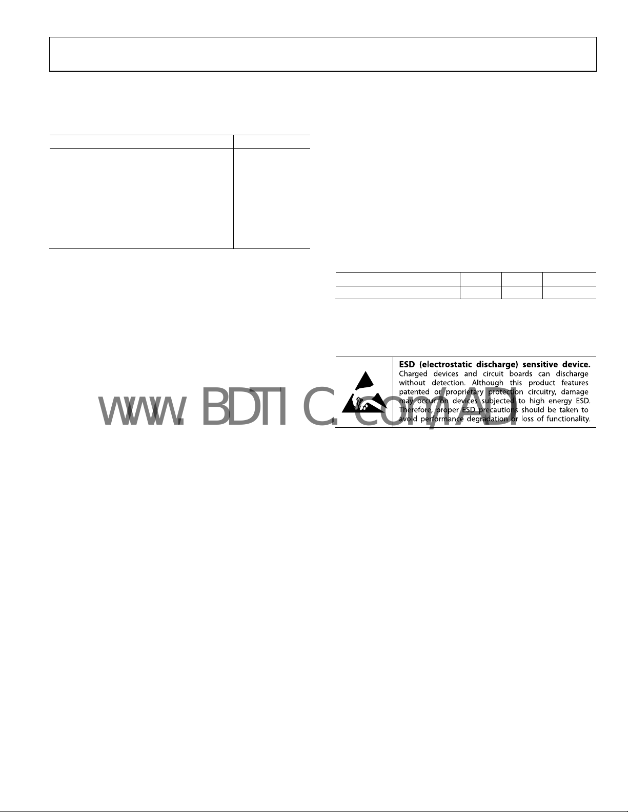
ABSOLUTE MAXIMUM RATINGS
Table 4.
Parameter Rating
Supply Voltage 6 V
Input Voltage +V
Differential Input Voltage1 ±V
Output Short-Circuit Duration to GND Indefinite
Storage Temperature Range (RJ Package) −65°C to +150°C
Operating Temperature Range −40°C to +85°C
Junction Temperature Range (RJ Package) −65°C to +150°C
Lead Temperature (Soldering, 10 sec) 300°C
1
Differential input voltage is limited to ±5.0 V, the supply voltage, or
whichever is less.
SUPPLY
SUPPLY
Stresses above those listed under Absolute Maximum Ratings
may cause permanent damage to the device. This is a stress
rating only; functional operation of the device at these or any
other conditions above those indicated in the operational
section of this specification is not implied. Exposure to absolute
maximum rating conditions for extended periods may affect
device reliability.
THERMAL RESISTANCE
θJA is specified for the worst-case conditions, that is, a device
soldered in a circuit board for surface-mount packages.
Table 5.
Package Type θ
8-Lead SOT-23 (RJ) 211.5 91.99 °C/W
1
θJA is specified for the nominal conditions, that is, θJA is specified for the
device soldered on a circuit board.
1
θJC Unit
JA
ESD CAUTION
Rev. 0 | Page 5 of 16
Page 6

AD8293G80/AD8293G160
A
www.BDTIC.com/ADI
PIN CONFIGURATION AND FUNCTION DESCRIPTIONS
AD8293Gxx
1
–IN
2
GND
3
REF
DC OUT
TOP VIEW
(Not to Scale)
Figure 3. Pin Configuration
8
+IN
+V
7
S
6
OUT
54
FILT
07451-003
Table 6. Pin Function Descriptions
Pin No. Mnemonic Description
1 −IN Inverting Input Terminal (True Differential Input)
2 GND Ground
3 REF Reference Voltage Terminal (Drive This Terminal to Level-Shift the Output)
4 ADC OUT Output with Series 5 kΩ Resistor for Use with an Antialiasing Filter
5 FILT Place a capacitor across FILT and OUT to limit the amount of switching noise at the output (see Applications Information)
6 OUT Output Terminal Without Integrated Filter
7 +VS Positive Power Supply Terminal
8 +IN Noninverting Input Terminal (True Differential Input)
Rev. 0 | Page 6 of 16
Page 7

AD8293G80/AD8293G160
www.BDTIC.com/ADI
TYPICAL PERFORMANCE CHARACTERISTICS
TA = 25°C, VCC = 5 V, and V
60
40
= VCC/2; G = 80, C2 = 1300 pF, and C3 = 39 nF; G = 160, C2 = 680 pF, and C3 = 39 nF, unless otherwise specified.
REF
G = 160
VCC = 2.7V, 5V
FILTER = 500Hz
60
G = 160
40
VCC = 2.7V, 5V
FILTER = 10kHz
20
GAIN (dB)
0
–20
–40
10 1 00 1k 10k 100k
G = 80
FREQUENCY (Hz)
Figure 4. Gain vs. Frequency
180
VCC = 2.7V, 5V
GAIN = 80, 160
160
FILT ER = 500Hz
140
120
100
CMR (dB)
80
60
40
20
10 100 1k 10k 1 00k
FREQUENCY (Hz)
Figure 5. Common-Mode Rejection (CMR) vs. Frequency
4
(0.02V, 3.3V)
3
VCC = 5V, V
REF
= VCC/2
(4.98V, 3.3V)
20
GAIN (dB)
0
–20
10 100 1k 10k 100k
07451-004
FREQUENCY (Hz)
G = 80
07451-007
Figure 7. Gain vs. Frequency
180
VCC = 2.7V, 5V
GAIN = 80, 160
160
FILT ER = 10kHz
140
120
100
CMR (dB)
80
60
40
20
10 100 1k 10k 100k
07451-005
FREQUENCY (Hz)
07451-008
Figure 8. Common-Mode Rejection (CMR) vs. Frequency
4
(0.02V, 3V)
3
(4.98V, 3V)
2
1
0
(0.02V, 0V) (4.98V, 0V)
INPUT COMMON-MODE VOLTAGE (V)
–1
–10123456
VCC = 2.7V,
V
REF
(2.68V, 1V)(0.02V, 1V)
= VCC/2
(2.68V, 0V)
OUTPUT VO LTAGE (V )
07451-018
Figure 6. Input Common-Mode Voltage Range vs. Output Voltage, G = 80
2
1
0
INPUT COMMON-MODE VO LTAGE (V)
–1
–10123456
(0.02V, 1V)
(0.02V, 0V)
VCC = 2.7V,
V
= VCC/2
REF
Figure 9. Input Common-Mode Voltage Range vs. Output Voltage, G = 160
Rev. 0 | Page 7 of 16
VCC = 5V, V
OUTPUT VO LTAGE (V )
= VCC/2
REF
(2.68V, 1V)
(2.68V, 0V)
(4.98V, 0V)
07451-019
Page 8

AD8293G80/AD8293G160
V
www.BDTIC.com/ADI
10
5
0
–5
–10
–15
INPUT OFFSET VOLTAGE (5mV/DIV)
–20
–25
–0.2 0 0.2 0. 4 0.6 0.8 1.0 1.2 1.4
POWER SUPPLY ON
GAIN = 160
GAIN = 80
TIME (ms)
4μV OFFSET
= 2.7V
V
CC
VCC = 5V
Figure 10. Input Offset Voltage vs. Turn-On Time, Filter = 500 Hz
1000
07451-010
10
POWER SUPPLY ON
5
4μV OFFSET
0
–5
–10
INPUT OFFSET VOLTAGE (5mV/DIV)
–15
–0.05 0 0.05 0.10 0.15 0.20
GAIN = 160
GAIN = 80
TIME (ms)
= 2.7V
V
CC
VCC = 5V
Figure 13. Input Offset Voltage vs. Turn-On Time, Filter = 10 kHz
07451-012
100
NOISE (nV/ Hz)
10
1
0.01 0.1 1 10 100 1k 10k 100k
FREQUENCY (Hz)
GAIN = 160
GAIN = 80
Figure 11. Voltage Noise Density
160
140
120
100
80
PSR (dB)
60
40
500Hz FILT ER
10kHz FILT ER
20
10 100 1k 10k 100k
GAIN = 160
GAIN = 80
FREQUENCY (Hz)
Figure 12. Power Supply Rejection (PSR) vs. Frequency
VOLTAGE NOISE (200nV/DIV)
TIME (10s/ DIV)
07451-009
07451-025
Figure 14. 0.01 Hz to 10 Hz Voltage Noise
0.30
VCC = 2.7V, 5V
G = 80, 160
0.25
0.20
0.15
10kHz FILT ER
0.10
0.05
50mV/DI
0
–0.05
500Hz FILT ER
–0.10
–0.15
07451-024
1ms/DIV
07451-011
Figure 15. Small Signal Step Response
Rev. 0 | Page 8 of 16
Page 9

AD8293G80/AD8293G160
V
V
www.BDTIC.com/ADI
VCC = 2.7V
G = 80, 160
VCC = 5V
G = 80, 160
10kHz FILT ER
500mV/DI
500Hz FILT ER
1ms/DIV
Figure 16. Large Signal Step Response
07451-013
10kHz FILTER
1V/DI
500Hz FILT ER
1ms/DIV
Figure 17. Large Signal Step Response
07451-017
Rev. 0 | Page 9 of 16
Page 10

AD8293G80/AD8293G160
V
www.BDTIC.com/ADI
THEORY OF OPERATION
The AD8293G80/AD8293G160 are precision current-mode
correction instrumentation amplifiers capable of single-supply
operation. The current-mode correction topology results in
excellent accuracy. Figure 18 shows a simplified diagram
illustrating the basic operation of the AD8293G80/AD8293G160
(without correction). The circuit consists of a voltage-to-current
amplifier (M1 to M6), followed by a current-to-voltage amplifier
(R2 and A1). Application of a differential input voltage forces a
current through External Resistor R1, resulting in conversion of
the input voltage to a signal current. Transistor M3 to Transistor
M6 transfer twice this signal current to the inverting input of
the op amp A1. Amplifier A1 and External Resistor R2 form
a current-to-voltage converter to produce a rail-to-rail output
voltage at V
OUT
.
Op amp A1 is a high precision auto-zero amplifier. This amplifier
preserves the performance of the autocorrecting, current-mode
amplifier topology while offering the user a true voltage-in,
voltage-out instrumentation amplifier. Offset errors are corrected
internally.
An external reference voltage is applied to the noninverting
input of A1 to set the output reference level. External Capacitor
C2 is used to filter out correction noise.
CC
V
INN
M5
M3 M4
I – I
R1
II
V
INP
2I
M1
R1
– V
INP
)
INN
R1
M2
2I
(V
I
=
R1
HIGH PSR AND CMR
Common-mode rejection and power supply rejection indicate
the amount that the offset voltage of an amplifier changes when
its common-mode input voltage or power supply voltage changes.
The autocorrection architecture of the AD8293G80/AD8293G160
continuously corrects for offset errors, including those induced
by changes in input or supply voltage, resulting in exceptional
rejection performance. The continuous autocorrection provides
great CMR and PSR performances over the entire operating
temperature range (−40°C to +85°C).
The parasitic resistance in series with R2 does not degrade CMR,
but causes a small gain error and a very small offset error.
Therefore, an external buffer amplifier is not required to drive
V
to maintain excellent CMR performance. This helps reduce
REF
system costs over conventional instrumentation amplifiers.
1/f NOISE CORRECTION
Flicker noise, also known as 1/f noise, is noise inherent in the
physics of semiconductor devices and decreases 10 dB per decade.
The 1/f corner frequency of an amplifier is the frequency at which
the flicker noise is equal to the broadband noise of the amplifier. At
lower frequencies, flicker noise dominates, causing large errors
in low frequency or dc applications.
Flicker noise is seen effectively as a slowly varying offset
error, which is reduced by the autocorrection topology of the
AD8293G80/AD8293G160. This allows the AD8293G80/
AD8293G160 to have lower noise near dc than standard low
noise instrumentation amplifiers.
C2
M6
I – I
I + I
R2
V
= V
R1
2I
R1
R1
V
BIAS
V
REF
OUT
R3
A1
2R2
V
– V
INP
+
REF
R1
C3
INN
07451-020
EXTERNAL
Figure 18. Simplified Schematic
Rev. 0 | Page 10 of 16
Page 11

AD8293G80/AD8293G160
V
V
www.BDTIC.com/ADI
APPLICATIONS INFORMATION
OVERVIEW
The AD8293G80/AD8293G160 reduce board area by integrating
filter components, such as Resistors R1, R2, and R3, as shown in
Figure 19. Two outputs are available to the user: OUT (Pin 6) and
ADC OUT (Pin 4). The difference between the two is the inclusion
of a series 5 k resistor at ADC OUT. With the addition of an
external capacitor, C3, ADC OUT forms a second filter, comprising
of the 5 k resistor and C3, which can be used as an ADC antialiasing filter. In contrast, OUT is the direct output of the instrumentation amplifier. When using the antialiasing filter, there is
slightly less switching ripple at ADC OUT than when obtaining
the signal directly from OUT.
+5
0.1µF
S
+IN
8
R1
4kΩ
–IN
1
Figure 19. AD8293G160 with Antialiasing Filter and Level-Shifted Output
(Using the Resistor Divider at the REF Pin, the Output Is Biased at 2.5 V)
REFERENCE CONNECTION
Unlike traditional 3-op-amp instrumentation amplifiers, parasitic
resistance in series with REF (Pin 3) does not degrade CMR
performance. The AD8293G80/AD8293G160 can attain extremely
high CMR performance without the use of an external buffer
amplifier to drive the REF pin, which is required by industrystandard instrumentation amplifiers. Reducing the need for
buffer amplifiers to drive the REF pin helps to save valuable
printed circuit board (PCB) space and minimizes system costs.
For optimal performance in single-supply applications, REF
should be set with a low noise precision voltage reference, such
as the ADR44x (see Figure 20). However, for a lower system cost,
the reference voltage can be set with a simple resistor voltage
divider between the supply and GND (see Figure 19). This
configuration results in degraded output offset performance if
the resistors deviate from their ideal values. In dual-supply
applications, V
The REF pin current is approximately 10 pA, and as a result, an
external buffer is not required.
REF
C2
680pF
7 5 6
IN-AMP
REFGND
32
FILT+V
R2
320kΩ
AD8293G160
100kΩ
OUT
5kΩ
R3
0.1µF
ADC OUT
100kΩ
OUTPUT TO ADC
WITH ANTI ALIASING
FILTER
4
C3
39nF
+5V
can simply be connected to GND.
07451-021
Rev. 0 | Page 11 of 16
+5
7
IN-AMP
REFGND
C2
5 6
FILT+V
R2
32
VOLTAGE
REFERENCE
0.1µF
OUTPUT
OUT
R3
5kΩ
ADC OUT
AD8293Gxx
4
1µF0.1µF
07451-022
0.1µF
S
+IN
8
R1
4kΩ
–IN
1
Figure 20. Operating on a Single Supply Using an External Voltage Reference
(The Output Can Be Used Without an Antialiasing Filter if the Signal
Bandwidth Is <10 Hz)
OUTPUT FILTERING
The output of the AD8293G80/AD8293G160 can be filtered to
reduce switching ripple. Two filters can be used in conjunction
to set the filter frequency. In the example that follows, two 700 Hz
filters are used in conjunction to form a 500 Hz (recommended)
bandwidth. Because the filter resistors are integrated in the
AD8293G80/AD8293G160, only external capacitors are needed
to set the filter frequencies.
The primary filter is needed to limit the amount of switching
noise at the output. Regardless of the output that is being used,
OUT or ADC OUT, the primary filter comprising R2 and C2
must be implemented. The R2 value depends on the model; Tabl e 7
shows the R2 value for each model.
Table 7. Internal R2 Values
Model R2 (kΩ)
AD8293G80 160
AD8293G160 320
The following equation results in the C2 value needed to set a
700 Hz primary filter. For a gain of 160, substitute R2 with
320 k; for a gain of 80, substitute R2 with 160 k.
C2 = 1/(700 × 2 × π × R2)
Adding an external capacitor, C3, and measuring the output from
ADC OUT further reduces the correction ripple. The internal
5 kΩ resistor, labeled R3 in Figure 18, forms a low-pass filter
with C3. This low-pass filter is the secondary filter. Set to
700 Hz, the secondary filter equation for C3 is as follows:
C3 = 1/(700 × 2 × π × 5 k)
Page 12

AD8293G80/AD8293G160
V
www.BDTIC.com/ADI
he addition of another single pole of 700 Hz on the output
T
(from the secondary filter in Figure 18) is required for bandwidt
hs
greater than 10 Hz. These two filters, together, produce an overall
bandwidth of 500 Hz. The internal resistors, R2 and R3, have an
absolute tolerance of 20%. Ta b le 8 lists the standard capacitors
needed to create a filter with an overall bandwidth of 500 Hz.
Table 8. Standard Capacitors Used to Form a Filter with an
Overall Bandwidth of 500 Hz
Model C2 (pF)
C3 (nF)
AD8293G80 1300 39
AD8293G160 680 39
For applications with low bandwi ths (<10 Hz), only the primary
d
filter is required. In such an event, the high frequency noise
from the auto-zero amplifier (output amplifier) is not filtered
before the following stage.
CLOCK FEEDTHROUG
The AD8293G80/AD8293G160
H
use two synchronized clocks
to perform the autocorrection. The input voltage-to-current
amplifiers are corrected at 60 kHz.
Trace amounts of these clock freque
ncies can be observed at
the OUT pin. The amount of visible correction feedthrough
is dependent on the values of the filters set by R2/C2. Use
ADC OUT to create a filter using R3/C3 to further reduce
correction feedthrough as described in the Output Filtering
section.
POWER SUPPLY BYPASSING
The AD8293G80/AD8293G160 use internally generated clock
signals to perform autocorrection. As a result, proper bypassing
is necessary to achieve optimum performance. Inadequate or
improper bypassing of the supply lines can lead to excessive
noise and offset voltage.
A 0.1 µF surface-mount capacitor should be connected between
the supply lines. This capacitor is necessary to minimize ripple
from the correction clocks inside the IC. For dual-supply operation,
a 0.1 µF (ceramic) surface-mount capacitor should be connected
from each supply pin to GND.
For single-supply operation, a 0.1 µF surface-mount capacitor
should be connected from the supply line to GND.
All bypass capacitors should be positioned as close to the DUT
supply pins as possible, especially the bypass capacitor between
the supplies. Placement of the bypass capacitor on the back of
the board directly under the DUT is preferred.
INPUT OVERVOLTAGE PROTECTION
All terminals of the AD8293G80/AD8293G160 are protected
against ESD. In the case of a dc overload voltage beyond either
supply, a large current would flow directly through the ESD
protection diodes. If such a condition can occur, an external resistor
should be used in series with the inputs to limit current for voltages
beyond the supply rails. The AD8293G80/AD8293G160 can safely
handle 5 mA of continuous current, resulting in an external
resistor selection of
R
= (VIN − VS)/5 mA
EXT
+5
C2
0.1µF
S
LOAD
I
R
1.8V
DC-DC
Figure 21. Measuring Current Through a Shunt Resistor (Filter Is Set to 500 Hz)
SHUNT
+IN
8
R1
4kΩ
–IN
1
1.3nF
7 5 6
FILT+V
R2
160kΩ
IN-AMP
REFGND
32
OUT
R3
5kΩ
ADC OUT
AD8293G80
4
C3
39nF
+3.3V
ADC
REF
0.1µF
10µF
07451-023
Rev. 0 | Page 12 of 16
Page 13

AD8293G80/AD8293G160
C
www.BDTIC.com/ADI
OUTLINE DIMENSIONS
2.90 BS
1.95
BSC
56
0.65 BSC
2.80 BSC
1.45 MAX
SEATING
PLANE
0.22
0.08
8°
4°
0°
0.60
0.45
0.30
1.60 BSC
PIN 1
INDICATOR
1.30
1.15
0.90
0.15 MAX
847
13
2
0.38
0.22
COMPLIANT TO JEDEC STANDARDS MO-178-BA
Figure 22. 8-Lead Small Outline Transistor Package [SOT-23]
(RJ-8)
Dimensions shown in millimeters
ORDERING GUIDE
Model Gain Temperature Range Package Description Package Option Branding
AD8293G80ARJZ-R21 80 −40°C to +85°C 8-Lead SOT-23 RJ-8 Y1H
AD8293G80ARJZ-R7
AD8293G80ARJZ-RL
AD8293G80BRJZ-R2
AD8293G80BRJZ-R7
AD8293G80BRJZ-RL
AD8293G160ARJZ-R2
AD8293G160ARJZ-R7
AD8293G160ARJZ-RL
AD8293G160BRJZ-R2
AD8293G160BRJZ-R7
AD8293G160BRJZ-RL
1
Z = RoHS Compliant Part.
1
80 −40°C to +85°C 8-Lead SOT-23 RJ-8 Y1H
1
80 −40°C to +85°C 8-Lead SOT-23 RJ-8 Y1H
1
80 −40°C to +85°C 8-Lead SOT-23 RJ-8 Y1N
1
80 −40°C to +85°C 8-Lead SOT-23 RJ-8 Y1N
1
80 −40°C to +85°C 8-Lead SOT-23 RJ-8 Y1N
1
160 −40°C to +85°C 8-Lead SOT-23 RJ-8 Y11
1
160 −40°C to +85°C 8-Lead SOT-23 RJ-8 Y11
1
160 −40°C to +85°C 8-Lead SOT-23 RJ-8 Y11
1
160 −40°C to +85°C 8-Lead SOT-23 RJ-8 Y1K
1
160 −40°C to +85°C 8-Lead SOT-23 RJ-8 Y1K
1
160 −40°C to +85°C 8-Lead SOT-23 RJ-8 Y1K
Rev. 0 | Page 13 of 16
Page 14

AD8293G80/AD8293G160
www.BDTIC.com/ADI
NOTES
Rev. 0 | Page 14 of 16
Page 15

AD8293G80/AD8293G160
www.BDTIC.com/ADI
NOTES
Rev. 0 | Page 15 of 16
Page 16

AD8293G80/AD8293G160
www.BDTIC.com/ADI
NOTES
©2008 Analog Devices, Inc. All rights reserved. Trademarks and
registered trademarks are the property of their respective owners.
D07451-0-8/08(0)
Rev. 0 | Page 16 of 16
 Loading...