

Page 1
Dual, Low Power
0.04
15
0.07
0.05
0.06
510
0.03
0.01
0.02
SUPPLY VOLTAGE – Volts
DIFFERENTIAL PHASE – Degrees
DIFFERENTIAL GAIN – Percent
DIFF GAIN
DIFF PHASE
a
FEATURES
Excellent Video Performance
Differential Gain & Phase Error of 0.01% & 0.05
High Speed
130 MHz 3 dB Bandwidth (G = +2)
450 V/s Slew Rate
80 ns Settling Time to 0.01%
Low Power
15 mA Max Power Supply Current
High Output Drive Capability:
50 mA Minimum Output Current per Amplifier
Ideal for Driving Back Terminated Cables
Flexible Power Supply
Specified for +5 V, 5 V and 15 V Operation
3.2 V Min Output Swing into a 150 Load
= 5 V)
(V
S
Excellent DC Performance
2.0 mV Input Offset Voltage
Available in 8-Lead SOIC and 8-Lead Plastic Mini-DIP
Video Op Amp
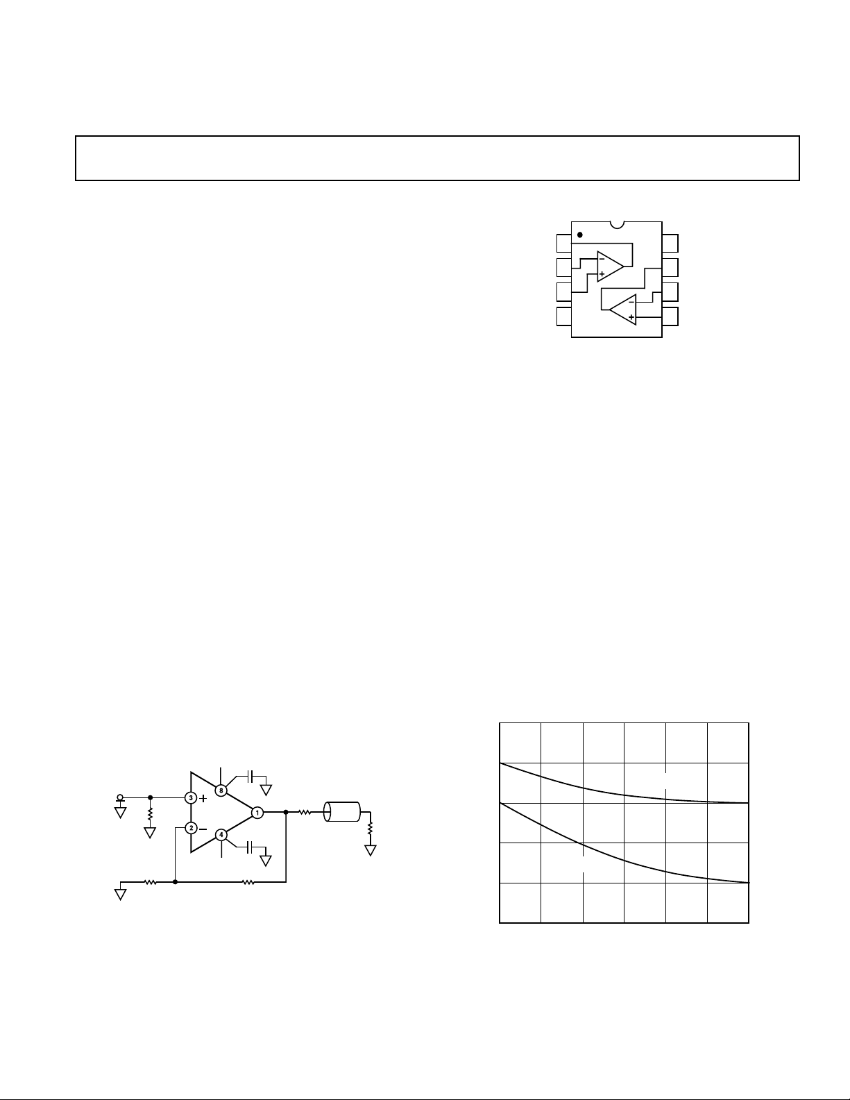
AD828
FUNCTIONAL BLOCK DIAGRAM
1
OUT1
–IN1
+IN1
V–
2
3
4
AD828
8
V+
7
OUT2
6
–IN2
+IN2
5
PRODUCT DESCRIPTION
The AD828 is a low cost, dual video op amp optimized for use
in video applications which require gains of +2 or greater and
high output drive capability, such as cable driving. Due to its
low power and single supply functionality, along with excellent
differential gain and phase errors, the AD828 is ideal for power
sensitive applications such as video cameras and professional
video equipment.
With video specs like 0.1 dB flatness to 40 MHz and low differential gain and phase errors of 0.01% and 0.05°, along with
50 mA of output current per amplifier, the AD828 is an excellent choice for any video application. The 130 MHz gain
bandwidth and 450 V/µs slew rate make the AD828 useful in
many high speed applications including: video monitors, CATV,
color copiers, image scanners and fax machines.
V
0.1F
R
75
V
IN
1k
R
75
T
1/2
AD828
–V
0.1F
1k
Figure 1. Video Line Driver
75
BT
R
T
75
REV. B
Information furnished by Analog Devices is believed to be accurate and
reliable. However, no responsibility is assumed by Analog Devices for its
use, nor for any infringements of patents or other rights of third parties
which may result from its use. No license is granted by implication or
otherwise under any patent or patent rights of Analog Devices.
The AD828 is fully specified for operation with a single +5 V
power supply and with dual supplies from ±5 V to ±15 V. This
power supply flexibility, coupled with a very low supply current
of 15 mA and excellent ac characteristics under all power supply
conditions, make the AD828 the ideal choice for many demanding yet power sensitive applications.
The AD828 is a voltage feedback op amp which excels as a gain
stage (gains >+2) or active filter in high speed and video systems
and achieves a settling time of 45 ns to 0.1%, with a low input
offset voltage of 2 mV max.
The AD828 is available in low cost, small 8-lead plastic miniDIP and SOIC packages.
Figure 2. Differential Phase vs. Supply Voltage
One Technology Way, P.O. Box 9106, Norwood, MA 02062-9106, U.S.A.
Tel: 781/329-4700 World Wide Web Site: http://www.analog.com
Fax: 781/326-8703 © Analog Devices, Inc., 2000
Page 2

AD828–SPECIFICATIONS
(@ TA = +25C, unless otherwise noted)
AD828
Parameter Conditions V
S
Min Typ Max Unit
DYNAMIC PERFORMANCE
–3 dB Bandwidth Gain = +2 ±5 V 60 85 MHz
±15 V 100 130 MHz
0, +5 V 30 45 MHz
Gain = –1 ±5 V 35 55 MHz
±15 V 60 90 MHz
0, +5 V 20 35 MHz
Bandwidth for 0.1 dB Flatness Gain = +2 ±5 V 30 43 MHz
= 1 pF ± 15 V 30 40 MHz
C
C
0, +5 V 10 18 MHz
Gain = –1 ±5 V 15 25 MHz
= 1 pF ± 15 V 30 50 MHz
C
Full Power Bandwidth
1
Slew Rate R
C
V
= 5 V p-p
OUT
= 500 Ω±5 V 22.3 MHz
R
LOAD
V
= 20 V p-p
OUT
= 1 kΩ±15 V 7.2 MHz
R
LOAD
1 kΩ±5 V 300 350 V/µs
LOAD
0, +5 V 10 19 MHz
Gain = –1 ±15 V 400 450 V/µs
0, +5 V 200 250 V/µs
Settling Time to 0.1% –2.5 V to +2.5 V ± 5 V 45 ns
0 V–10 V Step, A
= –1 ±15 V 45 ns
V
Settling Time to 0.01% –2.5 V to +2.5 V ±5 V 80 ns
0 V–10 V Step, AV = –1 ±15 V 80 ns
NOISE/HARMONIC PERFORMANCE
Total Harmonic Distortion F
= 1 MHz ±15 V –78 dB
C
Input Voltage Noise f = 10 kHz ±5 V, ± 15 V 10 nV/√Hz
Input Current Noise f = 10 kHz ±5 V, ± 15 V 1.5 pA/√Hz
Differential Gain Error NTSC ±15 V 0.01 0.02 %
= 150 Ω) Gain = +2 ±5 V 0.02 0.03 %
(R
L
0, +5 V 0.08 %
Differential Phase Error NTSC ±15 V 0.05 0.09 Degrees
= 150 Ω) Gain = +2 ±5 V 0.07 0.1 Degrees
(R
L
0, +5 V 0.1 Degrees
DC PERFORMANCE
Input Offset Voltage ±5 V, ± 15 V 0.5 2 mV
to T
T
MIN
MAX
3mV
Offset Drift 10 µV/°C
Input Bias Current ±5 V, ± 15 V 3.3 6.6 µA
T
T
MIN
MAX
10 µA
4.4 µA
Input Offset Current ±5 V, ± 15 V 25 300 nA
to T
T
MIN
MAX
500 nA
Offset Current Drift 0.3 nA/°C
Open Loop Gain V
= ±2.5 V ±5 V
OUT
= 500 Ω 3 5 V/mV
R
LOAD
T
to T
R
LOAD
V
OUT
R
LOAD
T
V
OUT
R
LOAD
MIN
MIN
MAX
= 150 Ω 2 4 V/mV
= ±10 V ±15 V
= 1 kΩ 5.5 9 V/mV
to T
MAX
= ±7.5 V ±15 V
= 150 Ω (50 mA Output) 3 5 V/mV
2 V/mV
2.5 V/mV
INPUT CHARACTERISTICS
Input Resistance 300 kΩ
Input Capacitance 1.5 pF
Input Common-Mode Voltage Range ±5 V +3.8 +4.3 V
–2.7 –3.4 V
±15 V +13 +14.3 V
–12 –13.4 V
0, +5 V +3.8 +4.3 V
+1.2 +0.9 V
Common-Mode Rejection Ratio V
= +2.5 V, T
CM
= ±12 V ±15 V 86 120 dB
V
CM
T
to T
MIN
MAX
MIN
to T
MAX
±5 V 82 100 dB
±15 V 84 100 dB
–2–
REV. B
Page 3
AD828
WARNING!
ESD SENSITIVE DEVICE
Parameter Conditions V
S
Min Typ Max Unit
OUTPUT CHARACTERISTICS
Output Voltage Swing R
= 500 Ω±5 V 3.3 3.8 ±V
LOAD
= 150 Ω±5 V 3.2 3.6 ±V
R
LOAD
R
= 1 kΩ±15 V 13.3 13.7 ±V
LOAD
= 500 Ω±15 V 12.8 13.4 ±V
R
LOAD
+1.5,
= 500 Ω 0, +5 V +3.5 ±V
R
LOAD
Output Current ±15 V 50 mA
±5 V 40 mA
0, +5 V 30 mA
Short-Circuit Current ±15 V 90 mA
Output Resistance Open Loop 8 Ω
MATCHING CHARACTERISTICS
Dynamic
Crosstalk f = 5 MHz ± 15 V –80 dB
Gain Flatness Match G = +1, f = 40 MHz ±15 V 0.2 dB
Skew Rate Match G = –1 ±15 V 10 V/µs
DC
Input Offset Voltage Match T
Input Bias Current Match T
Open-Loop Gain Match V
Common-Mode Rejection Ratio Match V
to T
MIN
MIN
O
CM
MAX
to T
MAX
= ±10 V, RL = 1 kΩ, T
= ±12 V, T
Power Supply Rejection Ratio Match ±5 V to ± 15 V, T
MIN
MIN
to T
to T
MIN
MAX
MAX
to T
±5 V, ± 15 V 0.5 2 mV
±5 V, ± 15 V 0.06 0.8 µA
±15 V 0.01 0.15 mV/V
MAX
±15 V 80 100 dB
80 100 dB
POWER SUPPLY
Operating Range Dual Supply ±2.5 ± 18 V
Single Supply +5 +36 V
Quiescent Current ±5 V 14.0 15 mA
to T
T
MIN
T
MIN
to T
MAX
MAX
Power Supply Rejection Ratio VS = ±5 V to ± 15 V, T
NOTES
1
Full power bandwidth = slew rate/2 π V
Specifications subject to change without notice.
PEAK
.
MIN
to T
MAX
±5 V 14.0 15 mA
±5 V 15 mA
80 90 dB
ORDERING GUIDE
Temperature Package Package
Model Range Description Option
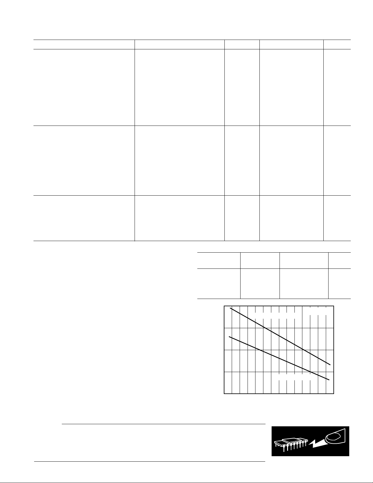
ABSOLUTE MAXIMUM RATINGS
Supply Voltage . . . . . . . . . . . . . . . . . . . . . . . . . . . . . . . . ±18 V
Internal Power Dissipation
2
1
Plastic DIP (N) . . . . . . . . . . . . . . . . . . See Derating Curves
Small Outline (R) . . . . . . . . . . . . . . . . . See Derating Curves
Input Voltage (Common Mode) . . . . . . . . . . . . . . . . . . . .±V
Differential Input Voltage . . . . . . . . . . . . . . . . . . . . . . . . ±6 V
Output Short Circuit Duration . . . . . . . . See Derating Curves
Storage Temperature Range (N, R) . . . . . . . –65°C to +125°C
AD828AN –40°C to +85°C 8-Lead Plastic DIP N-8
AD828AR –40°C to +85°C 8-Lead Plastic SOIC SO-8
AD828AR-REEL7 –40°C to +85°C 7" Tape & Reel SO-8
AD828AR-REEL –40°C to +85°C 13" Tape & Reel SO-8
S
2.0
8-LEAD MINI-DIP PACKAGE
1.5
TJ = +150C
Operating Temperature Range . . . . . . . . . . . –40°C to +85°C
Lead Temperature Range (Soldering 10 sec) . . . . . . . . +300°C
NOTES
1
Stresses above those listed under Absolute Maximum Ratings may cause perma-
nent damage to the device. This is a stress rating only; functional operation of the
device at these or any other conditions above those indicated in the operational
section of this specification is not implied. Exposure to absolute maximum rating
conditions for extended periods may affect device reliability.
2
Specification is for device in free air:
8-Lead Plastic DIP Package: θJA = 100°C/Watt
8-Lead SOIC Package: θJA = 155°C/Watt
1.0
0.5
8-LEAD SOIC PACKAGE
MAXIMUM POWER DISSIPATION – Watts
0
–50 90
–30
AMBIENT TEMPERATURE – C
50 703010–10 80–40 40 60200–20
Figure 3. Maximum Power Dissipation vs.
Temperature for Different Package Types
CAUTION
ESD (electrostatic discharge) sensitive device. Electrostatic charges as high as 4000 V readily
accumulate on the human body and test equipment and can discharge without detection.
Although the AD828 features proprietary ESD protection circuitry, permanent damage may
occur on devices subjected to high-energy electrostatic discharges. Therefore, proper ESD
precautions are recommended to avoid performance degradation or loss of functionality.
REV. B
–3–
Page 4
AD828–Typical Characteristics
20
15
+V
CM
10
–V
CM
5
INPUT COMMON-MODE RANGE – Volts
0
020
5
SUPPLY VOLTAGE – Volts
10
15
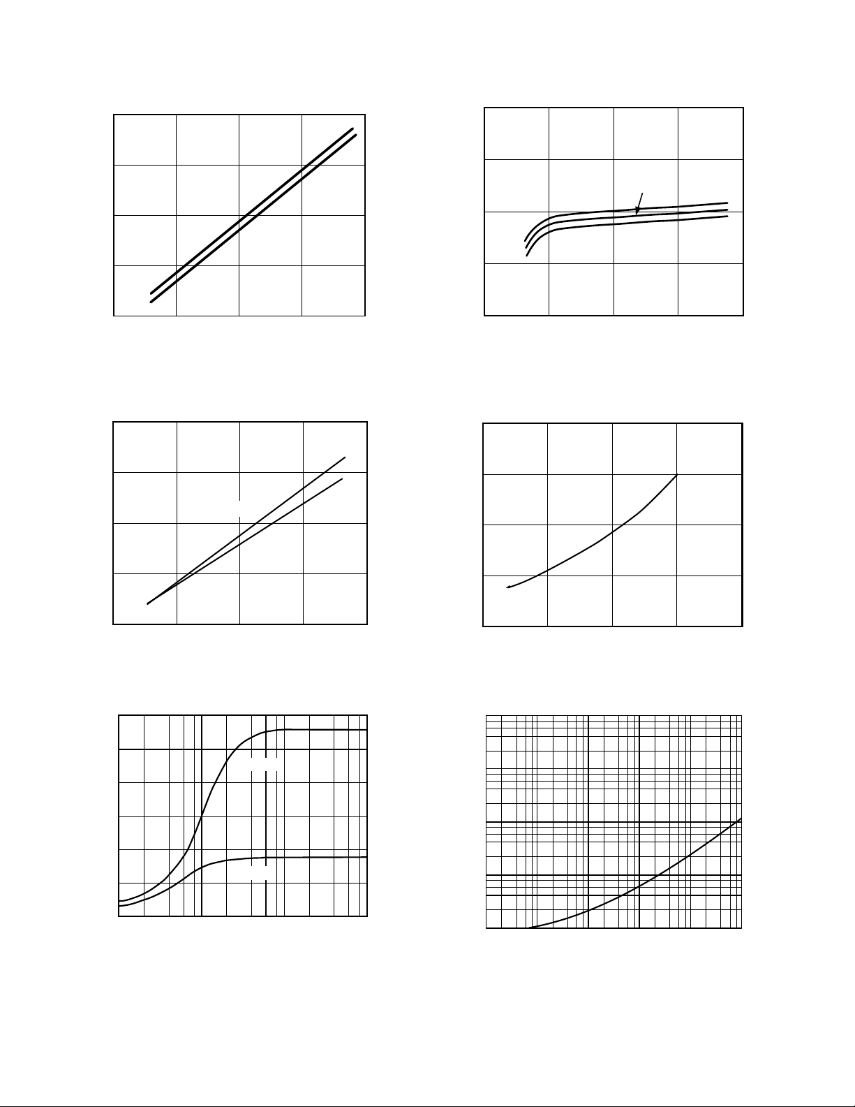
Figure 4. Common-Mode Voltage Range vs. Supply
Voltage
20
15
RL = 500
10
RL = 150
5
OUTPUT VOLTAGE SWING – Volts
7.7
7.2
+85°C
6.7
–40°C
6.2
QUIESCENT SUPPLY CURRENT PER AMP – mA
5.7
020
5
SUPPLY VOLTAGE – Volts
10
+25°C
15
Figure 7. Quiescent Supply Current per Amp vs. Supply
Voltage for Various Temperatures
500
450
400
SLEW RATE – V/s
350
0
020
5
SUPPLY VOLTAGE – Volts
10
15
Figure 5. Output Voltage Swing vs. Supply Voltage
30
25
20
15
10
5
OUTPUT VOLTAGE SWING – Volts p-p
0
10
100
Vs = 15V
Vs = 5V
1k
LOAD RESISTANCE –
10k
Figure 6. Output Voltage Swing vs. Load Resistance
300
Figure 8. Slew Rate vs. Supply Voltage
100
10
1
0.1
CLOSED-LOOP OUTPUT IMPEDANCE –
0.01
1k 100M10k
Figure 9. Closed-Loop Output Impedance vs. Frequency
SUPPLY VOLTAGE – Volts
100k 1M
FREQUENCY – Hz
20501510
10M
REV. B–4–
Page 5

AD828
g
7
6
5
4
3
INPUT BIAS CURRENT – A
2
1
–40
–60
TEMPERATURE – C
120806040 100200–20
Figure 10. Input Bias Current vs. Temperature
130
110
SOURCE CURRENT
90
SINK CURRENT
70
50
SHORT CIRCUIT CURRENT – mA
140
100
OPEN-LOOP GAIN – dB
–20
PHASE 5V OR
15V SUPPLIES
80
15V SUPPLIES
60
40
20
0
1k
RL = 1k
10k
5V SUPPLIES
100M10M1M100k
FREQUENCY – Hz
+100
+80
+60
+40
+20
0
1G
Figure 13. Open-Loop Gain and Phase Margin vs.
Frequency
9
8
7
6
5
OPEN-LOOP GAIN – V/mV
4
15V
5V
rees
PHASE MARGIN – De
30
–40
–60
TEMPERATURE – C
120100806040200–20
140
Figure 11. Short Circuit Current vs. Temperature
80
70
60
50
PHASE MARGIN – Degrees
40
–60 140
GAIN BANDWIDTH
–40
TEMPERATURE – C
PHASE MARGIN
100 120806040200–20
80
70
60
50
40
Figure 12. –3 dB Bandwidth and Phase Margin vs.
Temperature, Gain = +2
–3dB BANDWIDTH – MHz
3
100 1k 10k
LOAD RESISTANCE –
Figure 14. Open-Loop Gain vs. Load Resistance
100
90
PSR – dB
80
70
60
50
40
30
20
10
1k100
+SUPPLY
–SUPPLY
FREQUENCY – Hz
100M
10M1M100k10k
Figure 15. Power Supply Rejection vs. Frequency
REV. B
–5–
Page 6

AD828–Typical Characteristics
140
120
100
CMR – dB
80
60
1k 10M
10k
100k
FREQUENCY – Hz
1M
Figure 16. Common-Mode Rejection vs. Frequency
30
RL = 1k
20
–40
VIN = 1V p-p
GAIN = +2
–50
–60
–70
HARMONIC DISTORTION – dB
–100
–80
–90
100
1k
ND
HARMONIC
2
FREQUENCY – Hz
RD
HARMONIC
3
1M100k10k
Figure 19. Harmonic Distortion vs. Frequency
50
40
30
10M
10
OUTPUT VOLTAGE – Volts p-p
0
100k 1M 100M10M
RL = 150
FREQUENCY – Hz
Figure 17. Large Signal Frequency Response
10
8
6
4
2
0
–2
–4
–6
OUTPUT SWING FROM 0 TO ±V
–8
–10
0
1%
0.1%1%
0.1%
20
0.01%
0.01%
SETTLING TIME – ns
140120100806040
160
20
10
INPUT VOLTAGE NOISE – nV/ Hz
0
10
0
FREQUENCY – Hz
10M
1M100k10k1k100
Figure 20. Input Voltage Noise Spectral Density vs.
Frequency
650
550
450
SLEW RATE – V/s
350
250
–60 140
–40
TEMPERATURE – C
100 120806040200–20
Figure 18. Output Swing and Error vs. Settling Time
–6–
Figure 21. Slew Rate vs. Temperature
REV. B
Page 7

AD828
FREQUENCY – Hz
GAIN – dB
1.0
0
–1.0
100k 1M 100M10M
–0.2
–0.4
–0.6
–0.8
0.2
0.4
0.6
0.8
V
S
= 5V
V
S
= 5V
V
S
= 15V
10
8
6
1k
4
V
IN
2
0
GAIN – dB
–2
–4
–6
–8
–10
100k 1M 100M10M
1pF
1k
AD828
150
FREQUENCY – Hz
V
OUT
V
V
15V
5V
+5V
= 15V
S
= +5V
V
S
VS = 5V
S
0.1dB
FLATNESS
40MHz
43MHz
18MHz
Figure 22. Closed-Loop Gain vs. Frequency
DIFF GAIN
0.07
0.03
0.02
0.01
5
4
1k
3
V
IN
2
1
0
GAIN – dB
–1
–2
–3
–4
–5
100k 1M 100M10M
1pF
1k
AD828
150
V
OUT
FREQUENCY – Hz
V
S
15V
5V
+5V
= 5V
V
S
VS = +5V
0.1dB
FLATNESS
50MHz
25MHz
19MHz
V
= 15V
S
Figure 25. Closed-Loop Gain vs. Frequency, G = –1
0.06
0.05
0.04
DIFFERENTIAL PHASE – Degrees
510
Figure 23. Differential Gain and Phase vs. Supply Voltage
–30
–40
–50
–60
–70
–80
CROSSTALK – dB
–90
–100
–110
Figure 24. Crosstalk vs. Frequency
REV. B
DIFF PHASE
SUPPLY VOLTAGE – Volts
RL = 150
100k 100M10M1M10k
FREQUENCY – Hz
R
= 1k
L
DIFFERENTIAL GAIN – Percent
15
Figure 26. Gain Flatness Matching vs. Supply, G = +2
+5V
0.1F
1F
3
8
1/2
V
IN
AD828
2
USE GROUND PLANE
PINOUT SHOWN IS FOR MINIDIP PACKAGE
1
R
V
OUT
5
1/2
7
AD828
6
4
R
L
L
0.1F
1F
–5V
Figure 27. Crosstalk Test Circuit
–7–
Page 8

AD828–Typical Characteristics
C
F
1k
+V
S
3.3F
5V
100
90
50ns
HP PULSE (LS)
OR FUNCTION
(SS)
GENERATOR
Figure 28. Inverting Amplifier Connection
90
10
0%
100
0.01F
V
1k
IN
50
2
AD828
3
1/2
8
V
TEKTRONIX
OUT
1
0.01F
4
3.3F
–V
S
P6201 FET
R
L
PROBE
TEKTRONIX
7A24
PREAMP
10
0%
5V
Figure 31. Inverter Large Signal Pulse Response ±15 VS,
2V
50ns
= 1 pF, RL = 1 k
C
F
100
90
Ω
200mV
10ns
10
0%
2V
200mV
Figure 29. Inverter Large Signal Pulse Response ±5 VS,
= 1 pF, RL = 1 k
C
F
100
90
10
0%
Ω
200mV
200mV
10ns
Figure 30. Inverter Small Signal Pulse Response ±5 VS,
= 1 pF, RL = 150
C
F
Ω
Figure 32. Inverter Small Signal Pulse Response ±15 VS,
= 1 pF, RL= 1500
C
F
100
90
10
0%
200mV
200mV
Ω
10ns
Figure 33. Inverter Small Signal Pulse Response ±5 VS,
= 0 pF, RL = 150
C
F
Ω
–8–
REV. B
Page 9

HP PULSE (LS)
OR FUNCTION
(SS)
GENERATOR
AD828
C
F
1k
V
IN
100
50
1k
2
AD828
3
1/2
+V
3.3F
S
0.01F
8
V
OUT
TEKTRONIX
1
0.01F4
3.3F
–V
S
P6201 FET
R
L
PROBE
TEKTRONIX
7A24
PREAMP
5V
100
90
10
0%
5V
50ns
Figure 34. Noninverting Amplifier Connection
1V
100
90
10
0%
2V
50ns
Figure 35. Noninverting Large Signal Pulse Response
±
5 VS, CF = 1 pF, RL = 1 k
100mV
100
90
Ω
10ns
Figure 37. Noninverting Large Signal Pulse Response
±
15 VS, CF = 1 pF, RL = 1 k
100mV
100
90
10
0%
Ω
10ns
200mV
Figure 38. Noninverting Small Signal Pulse Response
±
15 VS, CF = 1 pF, RL = 150
100mV 10ns
100
90
Ω
10
0%
200mV
Figure 36. Noninverting Small Signal Pulse Response
±
5 VS, CF = 1 pF, RL = 150
Ω
REV. B
10
0%
200mV
Figure 39. Noninverting Small Signal Pulse Response
±
5 VS, CF = 0 pF, RL = 150
Ω
–9–
Page 10

AD828
THEORY OF OPERATION
The AD828 is a low cost, dual video operational amplifier
designed to excel in high performance, high output current video
applications.
The AD828 (Figure 40) consists of a degenerated NPN differential pair driving matched PNPs in a folded-cascode gain stage.
The output buffer stage employs emitter followers in a class AB
amplifier that delivers the necessary current to the load while
maintaining low levels of distortion.
The AD828 will drive terminated cables and capacitive loads of
10 pF or less. As the closed-loop gain is increased, the AD828
will drive heavier cap loads without oscillating.
+V
S
OUTPUT
–IN
+IN
–V
S
Figure 40. AD828 Simplified Schematic
INPUT CONSIDERATIONS
An input protection resistor (RIN in Figure 34) is required in circuits where the input to the AD828 will be subjected to transient
or continuous overload voltages exceeding the ±6 V maximum
differential limit. This resistor provides protection for the input
transistors by limiting their maximum base current.
For high performance circuits, it is recommended that a “balancing” resistor be used to reduce the offset errors caused by
bias current flowing through the input and feedback resistors.
The balancing resistor equals the parallel combination of R
IN
and RF and thus provides a matched impedance at each input
terminal. The offset voltage error will then be reduced by more
than an order of magnitude.
APPLYING THE AD828
The AD828 is a breakthrough dual amp that delivers precision
and speed at low cost with low power consumption. The AD828
offers excellent static and dynamic matching characteristics,
combined with the ability to drive heavy resistive loads.
As with all high frequency circuits, care should be taken to maintain overall device performance as well as their matching. The
following items are presented as general design considerations.
Circuit Board Layout
Input and output runs should be laid out so as to physically
isolate them from remaining runs. In addition, the feedback
resistor of each amplifier should be placed away from the feedback
resistor of the other amplifier, since this greatly reduces interamp
coupling.
Choosing Feedback and Gain Resistors
In order to prevent the stray capacitance present at each
amplifier’s summing junction from limiting its performance, the
feedback resistors should be ≤ 1 kΩ. Since the summing junction
capacitance may cause peaking, a small capacitor (1 pF–5 pF)
may be paralleled with Rf to neutralize this effect. Finally, sockets should be avoided, because of their tendency to increase
interlead capacitance.
Power Supply Bypassing
Proper power supply decoupling is critical to preserve the integrity of high frequency signals. In carefully laid out designs,
decoupling capacitors should be placed in close proximity to the
supply pins, while their lead lengths should be kept to a minimum. These measures greatly reduce undesired inductive effects
on the amplifier’s response.
Though two 0.1 µF capacitors will typically be effective in de-
coupling the supplies, several capacitors of different values can
be paralleled to cover a wider frequency range.
PARALLEL AMPS PROVIDE 100 mA TO LOAD
By taking advantage of the superior matching characteristics of
the AD828, enhanced performance can easily be achieved by
employing the circuit in Figure 41. Here, two identical cells are
paralleled to obtain even higher load driving capability than that
of a single amplifier (100 mA min guaranteed). R1 and R2 are
included to limit current flow between amplifier outputs that
would arise in the presence of any residual mismatch.
+V
1k
V
1k
1k
IN
1k
2
3
5
6
1/2
AD828
1/2
AD828
–V
S
1F
0.1F
R2
5
R1
5
V
OUT
R
L
8
1
7
4
0.1F
1F
S
Figure 41. Parallel Amp Configuration
–10–
REV. B
Page 11

AD828
3
2
1
1/2
AD828
8
0.1F
4
+15V
–15V
R
BT
75
R
T
75
V
IN
1k
1.0F
0.1F 1.0F
1k
75
R
T
75
A
IN
510
B
OUT
3
2
536
7
1/2
AD828
AD828
510
1/2
R
510
Z
100FT
RG59A/U
R
= 75
Z
1
6
5
Figure 42. Bidirectional Transmission CKT
Full-Duplex Transmission
Superior load handling capability (50 mA min/amp), high bandwidth, wide supply voltage range and excellent crosstalk
rejection makes the AD828 an ideal choice even for the most
demanding high speed transmission applications.
The schematic below shows a pair of AD828s configured to
drive 100 feet of coaxial cable in a full-duplex fashion.
Two different NTSC video signals are simultaneously applied at
A
and BIN and are recovered at A
IN
OUT
and B
, respectively.
OUT
This situation is illustrated in Figures 43 and 44. These pictures
R
510
Z
6
1
510
AD828
1/2
AD828
5
3 B
1/2
2
536
7
510
IN
A
OUT
clearly show that each input signal appears undisturbed at its
output, while the unwanted signal is eliminated at either receiver.
The transmitters operate as followers, while the receivers’ gain is
chosen to take full advantage of the AD828’s unparalleled CMRR.
(In practice this gain is adjusted slightly from its theoretical
value to compensate for cable nonidealities and losses.) R
is
Z
chosen to match the characteristic impedance of the cable
employed.
Finally, although a coaxial cable was used, the same topology
applies unmodified to a variety of cables (such, as twisted pairs
often used in telephony).
500mV
100
90
A
IN
B
OUT
10
0%
500mV
10µs
Figure 43. A Transmission/B Reception
B
IN
A
OUT
Figure 44. B Transmission/A Reception
90
10
0%
100
500mV
500mV
10µs
A High Performance Video Line Driver
The buffer circuit shown in Figure 45 will drive a backterminated 75 Ω video line to standard video levels (1 V p-p)
with 0.1 dB gain flatness to 40 MHz with only 0.05° and 0.01%
differential phase and gain at the 3.58 MHz NTSC subcarrier
frequency. This level of performance, which meets the requirements for high-definition video displays and test equipment, is
achieved using only 7 mA quiescent current/amplifier.
Figure 45. Video Line Driver
REV. B
–11–
Page 12

AD828
LOW DISTORTION LINE DRIVER
The AD828 can quickly be turned into a powerful, low distortion line driver (see Figure 46). In this arrangement the AD828
can comfortably drive a 75 Ω back-terminated cable, with a
5 MHz, 2 V p-p input; all of this while achieving the harmonic
distortion performance outlined in the following table.
Configuration 2nd Harmonic
1. No Load –78.5 dBm
2. 150 Ω RL Only –63.8 dBm
3. 150 Ω RL 7.5 Ω R
C
In this application one half of the AD828 operates at a gain of
2.1 and supplies the current to the load, while the other provides the overall system gain of 2. This is important for two
reasons: the first is to keep the bandwidth of both amplifiers the
same, and the second is to preserve the AD828’s ability to operate from low supply voltage. R
varies with the load and must
C
be chosen to satisfy the following equation:
RC = MR
where M is defined by [(M + 1) G
Gain, G
= System Gain.
S
S
–70.4 dBm
,
L
= GD] and GD = Driver's
1.1k
+V
3
AD828
2
6
AD828
5
1/2
1/2
S
1F
0.1F
8
1
R
C
1k
7
4
1F
0.1F
–V
S
7.5
75
R
L
75
C1823a–0–6/00 (rev. B) 00879
1k
1k
V
IN
75
Figure 46. Low Distortion Amplifier
8-Lead Plastic Mini-DIP (N) Package
0.165
(4.19
PIN 1
0.125
(3.18)
0.01
0.25)
MIN
0.018
(0.46
8
1
0.39 (9.91) MAX
0.003
0.08)
0.10
(2.54)
BSC
4
0.033
(0.84)
NOM
5
0.25
(6.35)
(7.87)
0.0350.01
(0.89
0.25)
0.18
(4.57
SEATING
PLANE
0.31
0.03
0.76)
OUTLINE DIMENSIONS
Dimensions shown in inches and (mm).
0.30 (7.62)
REF
0.0110.003
0.08)
(0.28
15
°
0
°
0.1574 (4.00)
0.1497 (3.80)
PIN 1
0.0098 (0.25)
0.0040 (0.10)
SEATING
0.1968 (5.00)
0.1890 (4.80)
85
0.0500 (1.27)
PLANE
8-Lead SO (R) Package
0.2440 (6.20)
0.2284 (5.80)
41
BSC
0.0192 (0.49)
0.0138 (0.35)
0.0688 (1.75)
0.0532 (1.35)
0.0098 (0.25)
0.0075 (0.19)
0.0196 (0.50)
0.0099 (0.25)
8
0.0500 (1.27)
0
0.0160 (0.41)
45
PRINTED IN U.S.A.
–12–
REV. B
 Loading...