

Page 1
Low Power, Wide Supply Range,
Low Cost Difference Amplifiers, G = ½, 2
FEATURES
Wide input range beyond supplies
Rugged input overvoltage protection
Low supply current: 200 µA maximum (per amplifier)
Low power dissipation: 0.5 mW at V
Bandwidth: 1 MHz (G = ½)
CMRR: 80 dB minimum, dc to 20 kHz (G = ½, B Grade)
Low offset voltage drift: ±1 V/°C maximum (B Grade)
Low gain drift: 1 ppm/°C maximum (B Grade)
Enhanced slew rate: 1.4 V/µs
Wide power supply range
Single supply: 2 V to 36 V
Dual supplies: ±2 V to ±18 V
8-lead SOIC, 14-lead SOIC, and 8-lead MSOP packages
APPLICATIONS
Voltage measurement and monitoring
Current measurement and monitoring
Instrumentation amplifier building block
Portable, battery-powered equipment
Test and measurement
GENERAL DESCRIPTION
The AD8278 and AD8279 are general-purpose difference
amplifiers intended for precision signal conditioning in power
critical applications that require both high performance and low
power. The AD8278 and AD8279 provide exceptional commonmode rejection ratio (80 dB) and high bandwidth while amplifying
input signals that are well beyond the supply rails. The on-chip
resistors are laser trimmed for excellent gain accuracy and high
CMRR. They also have extremely low gain drift vs. temperature.
The common-mode range of the amplifier extends to almost
triple the supply voltage (for G = ½), making the amplifer ideal
for single-supply applications that require a high commonmode voltage range. The internal resistors and ESD circuitry at
the inputs also provide overvoltage protection to the op amp.
The AD8278 and AD8279 can be used as difference amplifiers with
G = ½ or G = 2. They can also be connected in a high precision,
single-ended configuration for non inverting and inverting gains of
−½, −2, +3, +2, +1½, +1, or +½. The AD8278 and AD8279
provide an integrated precision solution that has a smaller size,
lower cost, and better performance than a discrete alternative.
The AD8278 and AD8279 operate on single supplies (2.0 V to 36 V)
or dual supplies (±2 V to ±18 V). The maximum quiescent supply
current is 200 A, which is ideal for battery-operated and portable
systems. For unity-gain difference amplifiers with similar
performance, refer to the AD8276 and AD8277 data sheets.
Rev. B
Information furnished by Analog Devices is believed to be accurate and reliable. However, no
responsibility is assumed by Analog Devices for its use, nor for any infringements of patents or other
rights of third parties that may result from its use. Specifications subject to change without notice. No
license is granted by implication or otherwise under any patent or patent rights of Analog Devices.
Trademarks and registered trademarks are the property of their respective owners.
= 2.5 V
S
AD8278/AD8279
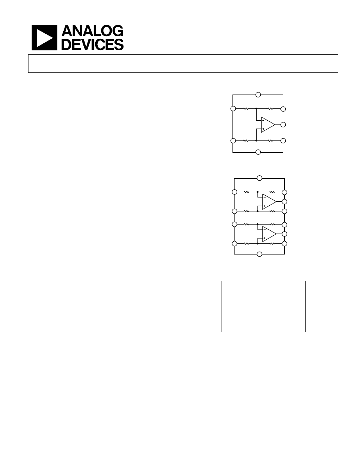
FUNCTIONAL BLOCK DIAGRAMS
+VS
7
40k 20k
2
–IN
40k
3 1
+IN
40k 20k
2
–INA
3 14
+INA
–INB
+INB
40k
40k 20k
6
5 8
40k
Table 1. Difference Amplifiers by Category
Low
Distortion
High Voltage Current Sens ing
AD8270 AD628 AD8202 (U) AD8276
AD8271 AD629 AD8203 (U) AD8277
AD8273 AD8205 (B)
AD8274 AD8206 (B)
AMP03 AD8216 (B)
1
U = unidirectional, B = bidirectional.
The AD8278 is available in the space-saving 8-lead MSOP and
SOIC packages, and the AD8279 is offered in a 14-lead SOIC
package. Both are specified for performance over the industrial
temperature range of −40°C to +85°C and are fully RoHS
compliant.
One Technology Way, P.O. Box 9106, Norwood, MA 02062-9106, U.S.A.
Tel: 781.329.4700 www.analog.com
Fax: 781.461.3113 ©2009–2010 Analog Devices, Inc. All rights reserved.
AD8278
20k
4
–VS
Figure 1. AD8278
+VS
11
AD8279
20k
20k
4
–VS
Figure 2. AD8279
5
SENSE
6
OUT
REF
12
SENSEA
13
OUTA
REFA
10
SENSEB
9
OUTB
REFB
1
Low Power
08308-001
08308-058
Page 2

AD8278/AD8279
TABLE OF CONTENTS
Features .............................................................................................. 1
Applications ....................................................................................... 1
General Description ......................................................................... 1
Functional Block Diagrams ............................................................. 1
Revision History ............................................................................... 2
Specifications ..................................................................................... 3
Absolute Maximum Ratings ............................................................ 7
Thermal Resistance ...................................................................... 7
Maximum Power Dissipation ..................................................... 7
Short-Circuit Current .................................................................. 7
ESD Caution .................................................................................. 7
Pin Configurations and Function Descriptions ........................... 8
REVISION HISTORY
4/10—Rev. A to Rev. B
Changed Supply Current Parameters to AD8278 Supply Current
Parameter and AD8279 Supply Current Parameter, Table 5 ...... 6
Updated Outline Dimensions ....................................................... 20
10/09—Rev. 0 to Rev. A
Added AD8279 and 14-Lead SOIC Model ..................... Universal
Changes to Features .......................................................................... 1
Changes to General Description .................................................... 1
Change to Table 2 ............................................................................. 3
Change to Table 3 ............................................................................. 4
Change to Table 4 ............................................................................. 5
Typical Performance Characteristics ..............................................9
Theory of Operation ...................................................................... 16
Circuit Information .................................................................... 16
Driving the AD8278 and AD8279 ........................................... 16
Input Voltage Range ................................................................... 16
Power Supplies ............................................................................ 17
Applications Information .............................................................. 18
Configurations ............................................................................ 18
Differential Output .................................................................... 19
Instrumentation Amplifier........................................................ 19
Outline Dimensions ....................................................................... 20
Ordering Guide .......................................................................... 21
Change to Table 5 .............................................................................. 6
Added Figure 6 and Table 9 ............................................................. 8
Changes to Figure 31 and Figure 32............................................. 13
Changes to Figure 40, Figure 41, and Figure 42 ......................... 14
Added Figure 47; Renumbered Sequentially .............................. 15
Changes to Figure 51 to Figure 57 ................................................ 18
Added Differential Output Section .............................................. 19
Changes to Figure 59 ...................................................................... 19
Updated Outline Dimensions ....................................................... 21
Changes to Ordering Guide .......................................................... 21
7/09—Revision 0: Initial Version
Rev. B | Page 2 of 24
Page 3

AD8278/AD8279
SPECIFICATIONS
VS = ±5 V to ±15 V, V
otherwise noted.
Table 2.
Parameter Conditions
INPUT CHARACTERISTICS
System Offset1 50 100 50 250 µV
Over Temperature TA = −40°C to +85°C 100 250 µV
vs. Power Supply VS = ±5 V to ±18 V 2.5 5 µV/V
Average Temperature
Coefficient T
Common-Mode Rejection
Ratio (RTI)
Input Voltage Range2 −3 (VS + 0.1) +3 (VS − 1.5) −3 (VS + 0.1) +3 (VS − 1.5) V
Impedance3
Differential 120 120 kΩ
Common Mode 30 30 kΩ
DYNAMIC PERFORMANCE
Bandwidth 1 1 MHz
Slew Rate 1.1 1.4 1.1 1.4 V/µs
Channel Separation f = 1 kHz 130 130 dB
Settling Time to 0.01% 10 V step on output,
Settling Time to 0.001% 10 10 µs
GAIN
Gain Error 0.005 0.02 0.01 0.05 %
Gain Drift TA = −40°C to +85°C 1 5 ppm/°C
Gain Nonlinearity V
OUTPUT CHARACTERISTICS
Output Voltage Swing4 V
Short-Circuit Current Limit ±15 ±15 mA
Capacitive Load Drive 200 200 pF
NOISE5
Output Voltage Noise f = 0.1 Hz to 10 Hz 1.4 1.4 V p-p
f = 1 kHz 47 50 47 50 nV/√Hz
POWER SUPPLY6
AD8278 Supply Current 200 200 A
Over Temperature TA = −40°C to +85°C 250 250 A
AD8279 Supply Current 300 350 300 350 A
Over Temperature TA = −40°C to +85°C 400 400 A
Operating Voltage Range7
TEMPERATURE RANGE
Operating Range −40 +125 −40 +125 °C
1
Includes input bias and offset current errors, RTO (referred to output).
2
The input voltage range may also be limited by absolute maximum input voltage or by the output swing. See the for details. Input Voltage Range
3
Internal resistors are trimmed to be ratio matched and have ±20% absolute accuracy.
4
Output voltage swing varies with supply voltage and temperature. See Figur through for details. e 22 Figure 25
5
Includes amplifier voltage and current noise, as well as noise from internal resistors.
6
Supply current varies with supply voltage and temperature. See Figure and for details. 26 Figure 28
7
Unbalanced dual supplies can be used, such as −VS = −0.5 V and +VS = +2 V. The positive supply rail must be at least 2 V above the negative supply and reference
voltage.
= 0 V, TA = 25°C, RL = 10 k connected to ground, G = ½ difference amplifier configuration, unless
REF
G = ½
Grade B Grade A
Min Typ Max Min Typ Max
= −40°C to +85°C 0.3 1 2 5 µV/°C
A
VS = ±15 V, VCM = ±27 V,
= 0 Ω 80 74 dB
R
S
= 100 pF
C
L
= 20 V p-p 7 12 ppm
OUT
= ±15 V, RL = 10 kΩ
S
= −40°C to +85°C −VS + 0.2 +VS − 0.2 −VS + 0.2 +VS − 0.2 V
T
A
9 9 µs
±2 ±18 ±2 ±18 V
Unit
Rev. B | Page 3 of 24
Page 4

AD8278/AD8279
VS = ±5 V to ±15 V, V
otherwise noted.
Table 3.
Parameter Conditions
INPUT CHARACTERISTICS
System Offset1 100 200 100 500 µV
Over Temperature TA = −40°C to +85°C 200 500 µV
vs. Power Supply VS = ±5 V to ±18 V 5 10 µV/V
Average Temperature
Coefficient
Common-Mode
Rejection Ratio (RTI)
Input Voltage Range2 −1.5 (VS + 0.1) +1.5 (VS − 1.5) −1.5 (VS + 0.1) +1.5 (VS − 1.5) V
Impedance3
Differential 120 120 kΩ
Common Mode 30 30 kΩ
DYNAMIC PERFORMANCE
Bandwidth 550 550 kHz
Slew Rate 1.1 1.4 1.1 1.4 V/µs
Channel Separation f = 1 kHz 130 130 dB
Settling Time to 0.01% 10 V step on output,
Settling Time to 0.001% 11 11 µs
GAIN
Gain Error 0.005 0.02 0.01 0.05 %
Gain Drift TA = −40°C to +85°C 1 5 ppm/°C
Gain Nonlinearity V
OUTPUT CHARACTERISTICS
Output Voltage Swing4 VS = ±15 V, RL = 10 kΩ,
Short-Circuit Current
Limit
Capacitive Load Drive 350 350 pF
NOISE5
Output Voltage Noise f = 0.1 Hz to 10 Hz 2.8 2.8 V p-p
f = 1 kHz 90 95 90 95 nV/√Hz
POWER SUPPLY6
AD8278 Supply Current 200 200 A
Over Temperature TA = −40°C to +85°C 250 250 A
AD8279 Supply Current 300 350 300 350 A
Over Temperature TA = −40°C to +85°C 400 400 A
Operating Voltage Range7
TEMPERATURE RANGE
Operating Range −40 +125 −40 +125 °C
1
Includes input bias and offset current errors, RTO (referred to output).
2
The input voltage range may also be limited by absolute maximum input voltage or by the output swing. See the section for details. Input Voltage Range
3
Internal resistors are trimmed to be ratio matched and have ±20% absolute accuracy.
4
Output voltage swing varies with supply voltage and temperature. See Figur through for details. e 22 Figure 25
5
Includes amplifier voltage and current noise, as well as noise from internal resistors.
6
Supply current varies with supply voltage and temperature. See Figure and for details. 26 Figure 28
7
Unbalanced dual supplies can be used, such as −VS = −0.5 V and +VS = +2 V. The positive supply rail must be at least 2 V above the negative supply and reference
voltage.
= 0 V, TA = 25°C, RL = 10 k connected to ground, G = 2 difference amplifier configuration, unless
REF
G = 2
Grade B Grade A
Min Typ Max Min Typ Max
= −40°C to +85°C 0.6 2 2 5 µV/°C
T
A
VS = ±15 V, VCM = ±27 V,
= 0 Ω 86 80 dB
R
S
= 100 pF
C
L
= 20 V p-p 7 12 ppm
OUT
= −40°C to +85°C
T
A
−V
+ 0.2 +VS − 0.2 −VS + 0.2 +VS − 0.2 V
S
10 10 µs
±15 ±15 mA
±2 ±18 ±2 ±18 V
Unit
Rev. B | Page 4 of 24
Page 5

AD8278/AD8279
VS = +2.7 V to <±5 V, V
otherwise noted.
Table 4.
Parameter Conditions
INPUT CHARACTERISTICS
System Offset1 75 150 75 250 µV
Over Temperature TA = −40°C to +85°C 150 250 µV
vs. Power Supply VS = ±5 V to ±18 V 2.5 5 µV/V
Average Temperature
Coefficient
Common-Mode Rejection
Ratio (RTI)
V
Input Voltage Range2 −3 (VS + 0.1) +3 (VS − 1.5) −3 (VS + 0.1) +3 (VS − 1.5) V
Impedance3
Differential 120 120 kΩ
Common Mode 30 30 kΩ
DYNAMIC PERFORMANCE
Bandwidth 870 870 kHz
Slew Rate 1.3 1.3 V/µs
Channel Separation f = 1 kHz 130 130 dB
Settling Time to 0.01% 2 V step on output,
GAIN
Gain Error 0.005 0.02 0.01 0.05 %
Gain Drift TA = −40°C to +85°C 1 5 ppm/°C
OUTPUT CHARACTERISTICS
Output Swing4 R
Short-Circuit Current Limit ±10 ±10 mA
Capacitive Load Drive 200 200 pF
NOISE5
Output Voltage Noise f = 0.1 Hz to 10 Hz 1.4 1.4 V p-p
f = 1 kHz 47 50 47 50 nV/√Hz
POWER SUPPLY6
AD8278 Supply Current TA = −40°C to +85°C 200 200 A
AD8279 Supply Current TA = −40°C to +85°C 375 375 A
Operating Voltage Range 2.0 36 2.0 36 V
TEMPERATURE RANGE
Operating Range −40 +125 −40 +125 °C
1
Includes input bias and offset current errors, RTO (referred to output).
2
The input voltage range may also be limited by absolute maximum input voltage or by the output swing. See the section for details. Input Voltage Range
3
Internal resistors are trimmed to be ratio matched and have ±20% absolute accuracy.
4
Output voltage swing varies with supply voltage and temperature. See Figur through for details. e 22 Figure 25
5
Includes amplifier voltage and current noise, as well as noise from internal resistors.
6
Supply current varies with supply voltage and temperature. See Figure and for details. 27 Figure 28
= midsupply, TA = 25°C, RL = 10 k connected to midsupply, G = ½ difference amplifier configuration, unless
REF
G = ½
Grade B Grade A
Min Typ Max Min Typ Max
= −40°C to +85°C 0.3 1 2 5 µV/°C
T
A
VS = 2.7 V, VCM = 0 V to
= 0 Ω 80 74 dB
2.4 V, R
S
= ±5 V, VCM = −10 V
S
to +7 V, R
= 0 Ω 80 74 dB
S
= 100 pF, VS = 2.7 V
C
L
= 10 kΩ,
L
= −40°C to +85°C −VS + 0.1 +VS − 0.15 −VS + 0.1 +VS − 0.15 V
T
A
7 7 µs
Unit
Rev. B | Page 5 of 24
Page 6

AD8278/AD8279
VS = +2.7 V to <±5 V, V
otherwise noted.
Table 5.
Parameter Conditions
INPUT CHARACTERISTICS
System Offset1 150 300 150 500 µV
Over Temperature TA = −40°C to +85°C 300 500 µV
vs. Power Supply VS = ±5 V to ±18 V 5 10 µV/V
Average Temperature
Coefficient
Common-Mode Rejection
Ratio (RTI)
V
Input Voltage Range2 −1.5 (VS + 0.1) +1.5 (VS − 1.5) −1.5 (VS + 0.1) +1.5 (VS − 1.5) V
Impedance3
Differential 120 120 kΩ
Common Mode 30 30 kΩ
DYNAMIC PERFORMANCE
Bandwidth 450 450 kHz
Slew Rate 1.3 1.3 V/µs
Channel Separation f = 1 kHz 130 130 dB
Settling Time to 0.01% 2 V step on output,
GAIN
Gain Error 0.005 0.02 0.01 0.05 %
Gain Drift TA = −40°C to +85°C 1 5 ppm/°C
OUTPUT CHARACTERISTICS
Output Swing4 R
Short-Circuit Current Limit ±10 ±10 mA
Capacitive Load Drive 200 200 pF
NOISE5
Output Voltage Noise f = 0.1 Hz to 10 Hz 2.8 2.8 V p-p
f = 1 kHz 94 100 94 100 nV/√Hz
POWER SUPPLY6
AD8278 Supply Current TA = −40°C to +85°C 200 200 A
AD8279 Supply Current TA = −40°C to +85°C 375 375 A
Operating Voltage Range 2.0 36 2.0 36 V
TEMPERATURE RANGE
Operating Range −40 +125 −40 +125 °C
1
Includes input bias and offset current errors, RTO (referred to output).
2
The input voltage range may also be limited by absolute maximum input voltage or by the output swing. See the section for details. Input Voltage Range
3
Internal resistors are trimmed to be ratio matched and have ±20% absolute accuracy.
4
Output voltage swing varies with supply voltage and temperature. See Figur through for details. e 22 Figure 25
5
Includes amplifier voltage and current noise, as well as noise from internal resistors.
6
Supply current varies with supply voltage and temperature. See Figure and for details. 27 Figure 28
= midsupply, TA = 25°C, RL = 10 k connected to midsupply, G = 2 difference amplifier configuration, unless
REF
G = 2
Grade B Grade A
Min Typ Max Min Typ Max
= −40°C to +85°C 0.6 2 3 5 µV/°C
T
A
VS = 2.7 V, VCM = 0 V
to 2.4 V, R
= ±5 V, VCM = −10 V
S
to +7 V, R
= 0 Ω 86 80 dB
S
= 0 Ω 86 80 dB
S
= 100 pF, VS = 2.7 V
C
L
= 10 kΩ,
L
= −40°C to +85°C −VS + 0.1 +VS − 0.15 −VS + 0.1 +VS − 0.15 V
T
A
9 9 µs
Unit
Rev. B | Page 6 of 24
Page 7
AD8278/AD8279
ABSOLUTE MAXIMUM RATINGS
2.0
Table 6.
Parameter Rating
Supply Voltage ±18 V
Maximum Voltage at Any Input Pin −VS + 40 V
Minimum Voltage at Any Input Pin +VS − 40 V
Storage Temperature Range −65°C to +150°C
Specified Temperature Range −40°C to +85°C
Package Glass Transition Temperature (TG) 150°C
Stresses above those listed under Absolute Maximum Ratings
may cause permanent damage to the device. This is a stress
rating only; functional operation of the device at these or any
other conditions above those indicated in the operational
section of this specification is not implied. Exposure to absolute
maximum rating conditions for extended periods may affect
device reliability.
THERMAL RESISTANCE
The θJA values in Tabl e 7 assume a 4-layer JEDEC standard
board with zero airflow.
Table 7. Thermal Resistance
Package Type θJA Unit
8-Lead MSOP 135 °C/W
8-Lead SOIC 121 °C/W
14-Lead SOIC 105 °C/W
MAXIMUM POWER DISSIPATION
The maximum safe power dissipation for the AD8278 and
AD8279 are limited by the associated rise in junction tempera-
ture (T
) on the die. At approximately 150°C, which is the glass
J
transition temperature, the properties of the plastic change.
Even temporarily exceeding this temperature limit may change
the stresses that the package exerts on the die, permanently shifting
the parametric performance of the amplifiers. Exceeding a
temperature of 150°C for an extended period may result in a
loss of functionality.
1.6
1.2
0.8
0.4
MAXIMUM POWER DISSIPATION (W)
0
–50 0–25 255075100125
Figure 3. Maximum Power Dissipation vs. Ambient Temperature
SHORT-CIRCUIT CURRENT
The AD8278 and AD8279 have built-in, short-circuit protection
that limits the output current (see Figure 29 for more information).
While the short-circuit condition itself does not damage the
part, the heat generated by the condition can cause the part to
exceed its maximum junction temperature, with corresponding
negative effects on reliability. Figure 3 and Figure 29, combined
with knowledge of the supply voltages and ambient temperature of
the part, can be used to determine whether a short circuit will
cause the part to exceed its maximum junction temperature.
ESD CAUTION
TJ MAX = 150°C
SOIC
= 121°C/W
JA
MSOP
= 135°C/W
JA
AMBIENT TEMERATURE (°C)
08308-002
Rev. B | Page 7 of 24
Page 8
AD8278/AD8279
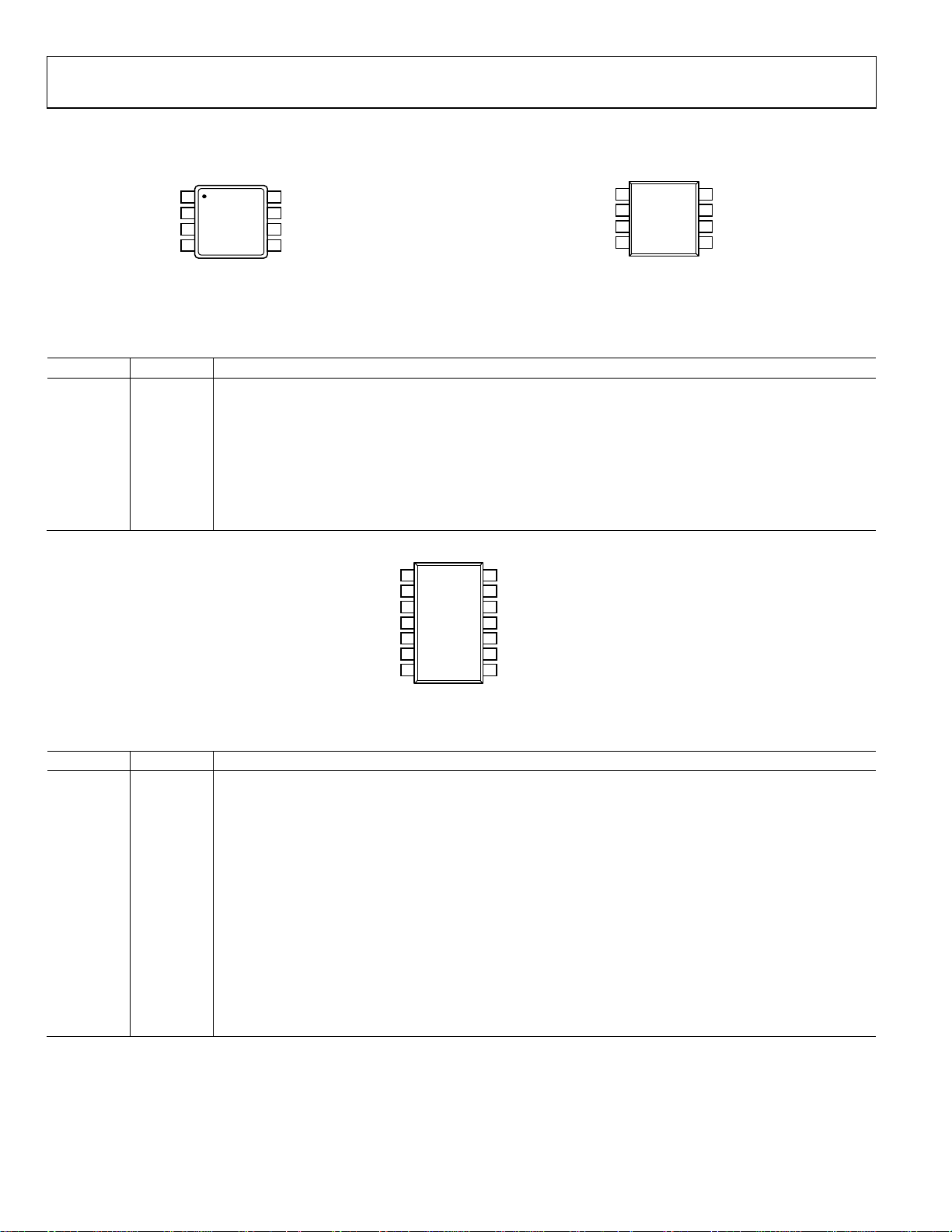
PIN CONFIGURATIONS AND FUNCTION DESCRIPTIONS
REF
REF
1
2
–IN
+IN
3
(Not to Scale)
–VS
4
NC = NO CONNECT
AD8278
TOP VIEW
8
7
6
5
NC
+VS
OUT
SENSE
8308-003
Figure 4. MSOP Pin Configuration
Table 8. AD8278 Pin Function Descriptions
Pin No. Mnemonic Description
1 REF Reference Voltage Input.
2 −IN Inverting Input.
3 +IN Noninverting Input.
4 −VS Negative Supply.
5 SENSE Sense Terminal.
6 OUT Output.
7 +VS Positive Supply.
8 NC No Connect.
1
AD8278
–IN
2
TOP VIEW
+IN
3
(Not to Scale)
4
–VS
NC = NO CONNECT
Figure 5. SOIC Pin Configuration
8
7
6
5
NC
+VS
OUT
SENSE
8308-004
1
NC
2
–INA
3
+INA
4
–VS
5 10
+INB
6 9
–INB
7 8
NC
NC = NO CONNECT
Figure 6. 14-Lead SOIC Pin Configuration
Table 9. AD8279 Pin Function Descriptions
Pin No. Mnemonic Description
1 NC No Connect.
2 −INA Channel A Inverting Input.
3 +INA Channel A Noninverting Input.
4 −VS Negative Supply.
5 +INB Channel B Noninverting Input.
6 −INB Channel B Inverting Input.
7 NC No Connect.
8 REFB Channel B Reference Voltage Input.
9 OUTB Channel B Output.
10 SENSEB Channel B Sense Terminal.
11 +VS Positive Supply.
12 SENSEA Channel A Sense Terminal.
13 OUTA Channel A Output.
14 REFA Channel A Reference Voltage Input.
AD8279
TOP VIEW
(Not to Scale)
14
13
12
11
REFA
OUTA
SENSEA
+VS
SENSEB
OUTB
REFB
08308-059
Rev. B | Page 8 of 24
Page 9

AD8278/AD8279
TYPICAL PERFORMANCE CHARACTERISTICS
VS = ±15 V, TA = 25°C, RL = 10 kΩ connected to ground, G = ½ difference amplifier configuration, unless otherwise noted.
600
500
400
300
200
NUMBER OF HITS
100
0
–150 –100 –50 0 50 100 150
SYSTEM OFFSET VOLTAGE (µV)
N = 3840
MEAN = –16.8
SD = 41.7673
Figure 7. Distribution of Typical System Offset Voltage, G = 2
800
700
600
500
400
300
NUMBER OF HITS
200
100
0
–60 –40 –20 0 20 40 60
CMRR (µV/V)
N = 3837
MEAN = 7.78
SD = 13.569
Figure 8. Distribution of Typical Common-Mode Rejection, G = 2
10
08308-005
08308-006
80
60
40
20
0
–20
–40
SYSTEM OFFSET (µV)
–60
–80
REPRESENTATIVE DATA
–100
–50 –35 –20 –5 10 25 40 55 70 85
TEMPERATURE (°C)
Figure 10. System Offset vs. Temperature, Normalized at 25°, G = ½
20
15
10
5
0
–5
–10
GAIN ERROR (µV/V)
–15
–20
–25
REPRESENTATIVE DATA
–30
–50 –35 –20 –5 10 25 40 55 70 85
TEMPERATURE (°C)
Figure 11. Gain Error vs. Temperature, Normalized at 25°C, G = ½
30
08308-008
08308-009
5
0
–5
CMRR (µV/V)
–10
–15
REPRESENTATIVE DATA
–20
–50–35–20–5102540557085
TEMPERATURE (° C)
Figure 9. CMRR vs. Temperature, Normalized at 25°C, G = ½
08308-007
Rev. B | Page 9 of 24
20
10
0
–10
COMMON-MODE VOLTAGE (V)
–20
–30
–20 –15 –10 –5 0 5 10 15 20
VS = ±5V
OUTPUT VOL TAGE (V)
VS = ±15V
Figure 12. Input Common-Mode Voltage vs. Output Voltage,
±15 V and ±5 V Supplies, G = ½
08308-010
Page 10

AD8278/AD8279
10
8
6
4
2
0
–2
–4
COMMON-MODE VOLTAGE (V)
–6
–8
–10
–0.5 0.5 1.5 2.5 3.5 4.5 5.5
VS = 2.7V
VS = 5V
OUTPUT VO LTAGE (V )
= MIDSUPPLY
V
REF
Figure 13. Input Common-Mode Voltage vs. Output Voltage,
5 V and 2.7 V Supplies, V
12
10
8
6
4
2
0
–2
COMMON-MODE VOLTAGE (V)
–4
–6
–0.5 0.5 1.5 2.5 3.5 4.5 5.5
VS = 2.7V
OUTPUT VO LTAGE (V )
= Midsupply, G = ½
REF
VS = 5V
V
= 0V
REF
Figure 14. Input Common-Mode Voltage vs. Output Voltage,
VS = ±5V
= 0 V, G = ½
REF
5 V and 2.7 V Supplies, V
30
20
10
0
–10
COMMON-MODE VOLTAGE (V)
–20
–30
–20 –15 –10 –5 0 10 20515
VS = ±15V
OUTPUT VOL TAGE (V)
Figure 15. Input Common-Mode Voltage vs. Output Voltage,
±15 V and ±5 V Supplies, G = 2
08308-011
08308-012
08308-013
5
4
3
2
1
0
–1
COMMON-MODE VOLTAGE (V)
–2
–3
–0.5 0.5 1.5 2.5 3.5 4.5 5.5
VS = 2.7V
VS = 5V
OUTPUT VO LTAGE (V )
V
= MIDSUPPLY
REF
Figure 16. Input Common-Mode Voltage vs. Output Voltage,
5 V and 2.7 V Supplies, V
6
5
4
3
2
1
0
COMMON-MODE VOLTAGE (V)
–1
–2
–0.5 0.5 1.5 2.5 3.5 4.5 5.5
VS = 2.7V
OUTPUT VO LTAGE (V )
= Midsupply, G = 2
REF
VS = 5V
V
REF
Figure 17. Input Common-Mode Voltage vs. Output Voltage,
= 0 V, G = 2
REF
18
12
GAIN = 2
6
0
GAIN = ½
–6
–12
GAIN (dB)
–18
–24
–30
–36
100 10M1M100k10k1k
5 V and 2.7 V Supplies, V
FREQUENCY (Hz)
Figure 18. Gain vs. Frequency, ±15 V Supplies
08308-014
= 0V
08308-015
08308-016
Rev. B | Page 10 of 24
Page 11

AD8278/AD8279
V
V
V
18
12
GAIN = 2
6
0
GAIN = ½
–6
–12
GAIN (dB)
–18
–24
–30
–36
100 10M1M100k10k1k
FREQUENCY (Hz)
Figure 19. Gain vs. Frequency, +2.7 V Single Supply
120
GAIN = 2
100
GAIN = ½
80
60
CMRR (dB)
40
20
0
11M100k10k1k10010
FREQUENCY (Hz)
Figure 20. CMRR vs. Frequency
120
08308-017
08308-018
+
S
–0.1
–0.2
–0.3
–0.4
TA = –40°C
TA = +25°C
TA = +85°C
+0.4
+0.3
OUTPUT VO LTAGE SWING (V)
+0.2
REFERRED TO SUPPLY VOLTAGES
+0.1
–V
S
2116141210864
SUPPLY VOLTAGE (±VS)
TA = +125°C
8
Figure 22. Output Voltage Swing vs. Supply Voltage and Temperature,
= 10 kΩ
R
L
+
S
–0.2
–0.4
–0.6
–0.8
–1.0
–1.2
+1.2
+1.0
+0.8
OUTPUT VOLTAGE SWING (V)
+0.6
REFERRED TO SUPPLY VOLTAGES
+0.4
+0.2
–V
S
2116141210864
SUPPLY VOLTAGE (±VS)
TA = –40°C
TA = +25°C
TA = +85°C
TA = +125°C
8
Figure 23. Output Voltage Swing vs. Supply Voltage and Temperature,
= 2 kΩ
R
L
+
S
08308-020
08308-021
100
80
60
PSRR (dB)
40
20
0
11M100k10k1k10010
–PSRR
+PSRR
FREQUENCY (Hz)
Figure 21. PSRR vs. Frequency
08308-019
–4
–8
+8
OUTPUT VOLTAGE SWING (V)
+4
REFERRED TO SUPPLY VOLTAGES
–V
S
1k 100k10k
LOAD RESIST ANCE ()
Figure 24. Output Voltage Swing vs. R
TA = –40°C
TA = +25°C
TA = +85°C
TA = +125°C
and Temperature, VS = ±15 V
L
08308-022
Rev. B | Page 11 of 24
Page 12

AD8278/AD8279
V
+
S
–0.5
–1.0
–1.5
–2.0
+2.0
+1.5
OUTPUT VOLTAGE SWING (V)
+1.0
REFERRED TO SUPPLY VOLTAGES
+0.5
–V
S
01987654321 0
Figure 25. Output Voltage Swing vs. I
180
170
160
150
140
SUPPLY CURRENT (µA)
130
120
01161412108642
OUTPUT CURRENT (mA)
and Temperature, VS = ±15 V
OUT
SUPPLY VOLTAGE (±V)
TA = –40°C
TA = +25°C
TA = +85°C
TA = +125°C
8
08308-024
Figure 26. Supply Current per Channel vs. Dual-Supply Voltage, VIN = 0 V
180
170
160
150
140
SUPPLY CURRENT (µA)
130
120
043530252015105
SUPPLY VOLTAGE (V)
0
08308-025
Figure 27. Supply Current per Channel vs. Single-Supply Voltage, VIN = 0 V,
V
= 0 V
REF
08308-023
250
200
150
VS = ±15V
100
SUPPLY CURRENT (µA)
50
0
–50 –30 –10 10 30 50 70 90 110 130
V
= +2.7V
S
TEMPERATURE (° C)
V
= MIDSUPPLY
REF
Figure 28. Supply Current per Channel vs. Temperature
30
25
20
15
10
5
0
–5
–10
SHORT-CIRCUIT CURRENT (mA)
–15
–20
–50 –30 –10 10 30 50 70 90 110 130
I
SHORT+
I
SHORT–
TEMPERATURE (° C)
Figure 29. Short-Circuit Current per Channel vs. Temperature
2.0
1.8
1.6
1.4
1.2
1.0
0.8
SLEW RATE (V/µ s)
0.6
0.4
0.2
0
–50 –30 –10 10 30 50 70 90 110 130
–SLEW RATE
+SLEW RATE
TEMPERATURE ( °C)
Figure 30. Slew Rate vs. Temperature, VIN = 20 V p-p, 1 kHz
08308-026
08308-027
08308-028
Rev. B | Page 12 of 24
Page 13

AD8278/AD8279
10
8
6
4
2
0
–2
–4
NONLINEARIT Y (2ppm/DI V)
–6
–8
–10
–5 –4 –3 –2 –1 0 1 2 3 4 5
OUTPUT VOLTAGE (V)
Figure 31. Gain Nonlinearity, V
20
16
12
8
4
0
–4
–8
NONLINEARIT Y (2ppm/DIV)
–12
–16
–20
–5 –4 –3 –2 –1 0 1 2 3 4 5
OU T PU T V OLTA G E ( V)
= ±15 V, RL ≥ 2 kΩ, G = ½
S
Figure 32. Gain Nonlinearity, VS = ±15 V, RL ≥ 2 kΩ, G = 2
08308-029
08308-030
1V/DIV
3.64µs TO 0. 01%
4.12µs TO 0 .001%
0.002%/DIV
4µs/DIV
TIME (µs)
8308-032
Figure 34. Large Signal Pulse Response and Settling Time, 2 V Step,
= 2.7 V, G = ½
V
S
5V/DIV
7.6µs TO 0.01%
9.68µs TO 0 .001%
0.002%/DIV
40µs/DIV
TIME (µs)
8308-033
Figure 35. Large Signal Pulse Response and Settling Time, 10 V Step,
V
= ±15 V, G = 2
S
5V/DIV
6.24µs TO 0. 01%
7.92µs TO 0 .001%
0.002%/DIV
40µs/DIV
TIME (µs)
8308-031
Figure 33. Large Signal Pulse Response and Settling Time, 10 V Step,
= ±15 V, G = ½
V
S
Rev. B | Page 13 of 24
1V/DIV
4.34µs TO 0. 01%
5.12µs TO 0 .001%
0.002%/DIV
4µs/DIV
TIME (µs)
08308-034
Figure 36. Large Signal Pulse Response and Settling Time, 2 V Step,
= 2.7 V
V
S
Page 14

AD8278/AD8279
V
V
V
V
5.0
VS = 5V
4.5
4.0
3.5
3.0
VS = 2.7V
2V/DI
10µs/DIV
Figure 37. Large Signal Step Response, G = ½
08308-035
2.5
2.0
1.5
OUTPUT VOLTAGE (V p-p)
1.0
0.5
0
100 1M100k10k1k
FREQUENCY (Hz)
Figure 40. Maximum Output Voltage vs. Frequency, V
= 5 V, 2.7 V
S
08308-038
5V/DI
10µs/DIV
08308-036
Figure 38. Large Signal Step Response, G = 2
30
VS = ±15V
25
20
15
VS = ±5V
10
OUTPUT VOLTAGE (V p-p)
5
0
100 1M100k10k1k
FREQUENCY (Hz)
Figure 39. Maximum Output Voltage vs. Frequency, VS = ±15 V, ±5 V
20mV/DI
NO LOAD
CL = 100pF
CL = 147pF
CL = 247pF
40µs/DIV
08308-039
Figure 41. Small Signal Step Response for Various Capacitive Loads, G = ½
20mV/DI
CL = 100pF
C
= 200pF
L
C
= 247pF
L
C
= 347pF
L
40µs/DIV
08308-037
08308-040
Figure 42. Small Signal Step Response for Various Capacitive Loads, G = 2
Rev. B | Page 14 of 24
Page 15

AD8278/AD8279
V
50
2k LOAD
GAIN = 2
GAIN = ½
1s/DIV
08308-044
45
40
35
30
25
20
OVERSHOOT (%)
15
10
5
0
02150 20010050
CAPACITIVE L OAD (pF)
±2V
±5V
±15V
±18V
50
Figure 43. Small Signal Overshoot vs. Capacitive Load, RL ≥ 2 kΩ, G = ½
35
30
25
20
15
OVERSHOOT (%)
10
5
±5V
±2V
±15V
±18V
1µV/DI
08308-041
Figure 46. 0.1 Hz to 10 Hz Voltage Noise
160
140
120
100
80
60
40
CHANNEL SEPARATION (dB)
20
0
0350150 250 30020010050
CAPACITIVE L OAD (pF)
Figure 44. Small Signal Overshoot vs. Capacitive Load, R
1k
100
NOISE (nV/ Hz)
10
0.1 100k10k1k100101
GAIN = 2
GAIN = ½
FREQUENCY (Hz)
Figure 45. Voltage Noise Density vs. Frequency
≥ 2 kΩ, G = 2
L
0
10 100 1k 10k 100k
08308-042
FREQUENCY ( Hz)
08308-060
Figure 47. Channel Separation
08308-043
Rev. B | Page 15 of 24
Page 16

AD8278/AD8279
THEORY OF OPERATION
CIRCUIT INFORMATION
Each channel of the AD8278 and AD8279 consists of a low power,
low noise op amp and four laser-trimmed on-chip resistors.
These resistors can be externally connected to make a variety
of amplifier configurations, including difference, noninverting,
and inverting configurations. Taking advantage of the integrated
resistors of the AD8278 and AD8279 provides the designer with
several benefits over a discrete design, including smaller size,
lower cost, and better ac and dc performance.
+VS
7
40k 20k
2
–IN
40k
3 1
+IN
Figure 48. Functional Block Diagram
DC Performance
Much of the dc performance of op amp circuits depends on the
accuracy of the surrounding resistors. Using superposition to
analyze a typical difference amplifier circuit, as is shown in
Figure 49, the output voltage is found to be
⎛
R2
⎜
VV
=
OUT
⎜
+
⎝
This equation demonstrates that the gain accuracy and commonmode rejection ratio of the AD8278 and AD8279 is determined
primarily by the matching of resistor ratios. Even a 0.1%
mismatch in one resistor degrades the CMRR to 69 dB for a
G = 2 difference amplifier.
The difference amplifier output voltage equation can be reduced to
R4
V
OUT
()
R3
as long as the following ratio of the resistors is tightly matched:
R4
R2
R1
=
R3
The resistors on the AD8278 and AD8279 are laser trimmed to
match accurately. As a result, the AD8278 and AD8279 provide
superior performance over a discrete solution, enabling better
CMRR, gain accuracy, and gain drift, even over a wide temperature range.
AD8278
5
SENSE
6
OUT
20k
4
–VS
⎞
R4
⎛
⎟
+
1
⎜
⎟
R2R1
VV
R3
⎝
⎠
−+−=ININ
REF
08308-045
R4
⎞
⎞
⎟
⎠
⎛
−
V
⎟
⎜
−+
ININ
R3
⎠
⎝
AC Performance
Component sizes and trace lengths are much smaller in an IC
than on a PCB; therefore, the corresponding parasitic elements
are also smaller. This results in better ac performance of the
AD8278 and AD8279. For example, the positive and negative
input terminals of the AD8278 and AD8279 op amps are
intentionally not pinned out. By not connecting these nodes to
the traces on the PCB, their capacitance remains low and
balanced, resulting in improved loop stability and excellent
common-mode rejection over frequency.
DRIVING THE AD8278 AND AD8279
Care should be taken to drive the AD8278 and AD8279 with a
low impedance source, for example, another amplifier. Source
resistance of even a few kilohms (kΩ) can unbalance the resistor
ratios and, therefore, significantly degrade the gain accuracy and
common-mode rejection of the AD8278 and AD8279. Because all
configurations present several kilohms (kΩ) of input resistance,
the AD8278 and AD8279 do not require a high current drive
from the source and are easy to drive.
INPUT VOLTAGE RANGE
The AD8278 and AD8279 are able to measure input voltages
beyond the supply rails. The internal resistors divide down
the voltage before it reaches the internal op amp and provide
protection to the op amp inputs. Figure 49 shows an example
of how the voltage division works in a difference amplifier
configuration. For the AD8278 and AD8279 to measure correctly,
the input voltages at the input nodes of the internal op amp
must stay below 1.5 V of the positive supply rail and can exceed
the negative supply rail by 0.1 V. Refer to the Power Supplies
section for more details.
R2
(V
)
IN+
R1 + R2
R3
V
IN–
R1
V
IN+
Figure 49. Voltage Division in the Difference Amplifier Configuration
R2
The AD8278 and AD8279 have integrated ESD diodes at the inputs
that provide overvoltage protection. This feature simplifies
system design by eliminating the need for additional external
protection circuitry and enables a more robust system.
The voltages at any of the inputs of the parts can safely range
from +V
− 40 V up to −VS + 40 V. For example, on ±10 V
S
supplies, input voltages can go as high as ±30 V. Care should be
taken to not exceed the +V
− 40 V to −VS + 40 V input limits
S
to avoid damaging the parts.
R2
R1 + R2
R4
(V
)
IN+
08308-062
Rev. B | Page 16 of 24
Page 17

AD8278/AD8279
POWER SUPPLIES
The AD8278 and AD8279 operate extremely well over a very
wide range of supply voltages. They can operate on a single
supply as low as 2 V and as high as 36 V, under appropriate
setup conditions.
For best performance, the user should ensure that the internal
op amp is biased correctly. The internal input terminals of the
op amp must have sufficient voltage headroom to operate
properly. Proper operation of the part requires at least 1.5 V
between the positive supply rail and the op amp input terminals.
This relationship is expressed in the following equation:
R1
+
R2R1
REF
VV
For example, when operating on a +V
V
= 0 V, it can be seen from Figure 50 that the op amp input
REF
terminals are biased at 0 V, allowing more than the required 1.5 V
headroom. However, if V
input terminals of the op amp are biased at 0.66 V (G = ½). Now
the op amp does not have the required 1.5 V headroom and
cannot function. Therefore, the user must increase the supply
voltage or decrease V
to restore proper operation.
REF
V5.1−+<
S
REF
= 2 V single supply and
S
= 1 V under the same conditions, the
The AD8278 and AD8279 are typically specified at single and
dual supplies, but they can be used with unbalanced supplies as
well; for example, −V
= −5 V, +VS = +20 V. The difference between
S
the two supplies must be kept below 36 V. The positive supply
rail must be at least 2 V above the negative supply.
R1
(V
)
REF
R1 + R2
R3
R1
R2
V
REF
Figure 50. Ensure Sufficient Voltage Headroom on the Internal Op Amp
R1 + R2
Inputs
R4
R1
(V
)
REF
08308-046
Use a stable dc voltage to power the AD8278 and AD8279. Noise
on the supply pins can adversely affect performance. Place a
bypass capacitor of 0.1 µF between each supply pin and ground,
as close as possible to each supply pin. Use a tantalum capacitor
of 10 µF between each supply and ground. It can be farther
away from the supply pins and, typically, it can be shared by
other precision integrated circuits.
Rev. B | Page 17 of 24
Page 18

AD8278/AD8279
V
V
V
APPLICATIONS INFORMATION
CONFIGURATIONS
The AD8278 and AD8279 can be configured in several ways (see
Figure 51 to Figure 57). These configurations have excellent
gain accuracy and gain drift because they rely on the internal
matched resistors. Note that Figure 53 shows the AD8278 and
AD8279 as difference amplifiers with a midsupply reference
voltage at the noninverting input. This allows the AD8278 and
AD8279 to be used as a level shifter, which is appropriate in
single-supply applications that are referenced to midsupply.
Tabl e 10 lists several single-ended amplifier configurations that
are not illustrated.
40k
2
–IN
40k 20k
3
+IN
V
= ½ (V
OUT
Figure 51. Difference Amplifier, Gain = ½
20k
5
–IN
20k 40k
1
+IN
V
= 2(V
OUT
IN+
Figure 52. Difference Amplifier, Gain = 2
40k
2
–IN
40k 20k
3
+IN
AD8278
= ½ (V
IN+
V
OUT
Figure 53. Difference Amplifier, Gain = ½, Referenced to Midsupply
AD8278
V
IN+
AD8278
V
IN
20k
) + V
IN
20k
5
OUT
6
1
)
IN
40k
2
6
3
)
5
OUT
6
1
V
= MIDSUPPLY
REF
REF
OUT
08308-047
08308-048
08308-049
Figure 54. Difference Amplifier, Gain = 2, Referenced to Midsupply
–IN
+IN
OUT
= 2 (V
IN
20k
5
20k 40k
1
IN+
2
1
3
AD8278
V
) + V
IN
40k
20k
40k
40k
REF
20k
2
OUT
6
3
V
= MIDSUPPLY
REF
5
6
OUT
AD8278
V
= –½V
OUT
IN
8308-051
Figure 55. Inverting Amplifier, Gain = −½
40k
25
20k
1
IN
40k
3
20k
OUT
6
AD8278
= 1.5V
V
OUT
IN
Figure 56. Noninverting Amplifier, Gain = 1.5
5
1
IN
20k
20k 40k
40k
2
OUT
6
3
AD8278
= 2V
OUT
IN
Figure 57. Noninverting Amplifier, Gain = 2
08308-050
08308-052
8308-053
Table 10. AD8278 Difference and Single-Ended Amplifier Configurations
Amplifier Configuration Signal Gain Pin 1 (REF) Pin 2 (VIN−) Pin 3 (VIN+) Pin 5 (SENSE)
Difference Amplifier +½ GND IN− IN+ OUT
Difference Amplifier +2 IN+ OUT GND IN−
Single-Ended Inverting Amplifier −½ GND IN GND OUT
Single-Ended Inverting Amplifier −2 GND OUT GND IN
Single-Ended Noninverting Amplifier +3⁄2 IN GND IN OUT
Single-Ended Noninverting Amplifier +3 IN OUT IN GND
Single-Ended Noninverting Amplifier +½ GND GND IN OUT
Single-Ended Noninverting Amplifier +1 IN GND GND OUT
Single-Ended Noninverting Amplifier +1 GND OUT IN GND
Single-Ended Noninverting Amplifier +2 IN OUT GND GND
Rev. B | Page 18 of 24
Page 19

AD8278/AD8279
The reference must be driven with a low impedance source to
maintain the internal resistor ratio. An example using the low
power, low noise OP1177 as a reference is shown in Figure 58.
INCORRECT
AD8278
REF
V
Figure 58. Driving the Reference Pin
V
CORRECT
AD8278
+
OP1177
–
REF
8308-054
DIFFERENTIAL OUTPUT
The two difference amplifiers of the AD8279 can be configured
to provide a differential output, as shown in Figure 59. This
differential output configuration is suitable for various applications,
such as strain gage excitation and single-ended-to-differential
conversion. The differential output voltage has a gain twice that
of a single AD8279 channel, as shown in the following equation:
V
If the AD8279 amplifiers are each configured for G = ½, the
differential gain is 1×; if the AD8279 amplifiers are each
configured for G = 2, the differential gain is 4×.
DIFF_OUT
–IN
+IN
= V
− V
+OUT
−OUT
+VS
20k 40k
12
20k
14 3
20k 40k
10
= 2 × G
11
AD8279
40k
AD8279
× (V
2
13
6
IN+
– V
+OUT
IN−
)
INSTRUMENTATION AMPLIFIER
The AD8278 and AD8279 can be used as building blocks for a
low power, low cost instrumentation amplifier. An instrumentation
amplifier provides high impedance inputs and delivers high
common-mode rejection. Combining the AD8278 with an Analog
Devices, Inc., low power amplifier (see Ta b le 1 1 ) creates a precise,
power efficient voltage measurement solution suitable for power
critical systems.
–IN
R
+IN
Figure 60. Low Power Precision Instrumentation Amplifier
Table 11. Low Power Op Amps
Op Amp (A1, A2) Features
AD8506 Dual micropower op amp
AD8607 Precision dual micropower op amp
AD8617 Low cost CMOS micropower op amp
AD8667 Dual precision CMOS micropower op amp
It is preferable to use dual op amps for the high impedance inputs
because they have better matched performance and track each
other over temperature. The AD8278 and AD8279 difference
amplifiers cancel out common-mode errors from the input op
amps, if they track each other. The differential gain accuracy of
the in-amp is proportional to how well the input feedback
resistors (R
increases as the differential gain is increased (1 + 2R
higher gain also reduces the common-mode voltage range.
Refer to
A Designer’s Guide to Instrumentation Amplifiers for
more design ideas and considerations at www.analog.com,
under Technical Documentation.
A1
R
F
G
R
F
A2
) match each other. The CMRR of the in-amp
F
20k
20k
40k
V
= (1 + 2RF/RG) (V
OUT
REF
40k
AD8278/
AD8279
IN+
– V
IN–
V
) × 2
F/RG
OUT
), but a
08308-056
20k
8 5
40k
4
–VS
Figure 59. AD8279 Differential Output G = 4 Configuration
9
–OUT
08308-061
Rev. B | Page 19 of 24
Page 20

AD8278/AD8279
OUTLINE DIMENSIONS
5.00 (0.1968)
4.80 (0.1890)
4.00 (0.1574)
3.80 (0.1497)
0.25 (0.0098)
0.10 (0.0040)
COPLANARITY
0.10
CONTROLLING DIMENSIONS ARE IN MILLIMETERS; INCH DIMENSIONS
(IN PARENTHESES) ARE ROUNDED-OFF MILLIMETER EQUIVALENTS FOR
REFERENCE ONLY AND ARE NOT APPROPRIATE FOR USE IN DESIGN.
85
1
1.27 (0.0500)
SEATING
PLANE
COMPLIANT TO JEDEC STANDARDS MS-012-AA
BSC
6.20 (0.2441)
5.80 (0.2284)
4
1.75 (0.0688)
1.35 (0.0532)
0.51 (0.0201)
0.31 (0.0122)
8°
0°
0.25 (0.0098)
0.17 (0.0067)
0.50 (0.0196)
0.25 (0.0099)
1.27 (0.0500)
0.40 (0.0157)
45°
012407-A
Figure 61. 8-Lead Standard Small Outline Package [SOIC_N]
Narrow Body (R-8)
Dimensions shown in millimeters and (inches)
3.20
3.00
2.80
8
5
3.20
3.00
2.80
PIN 1
IDENTIFIER
0.95
0.85
0.75
0.15
0.05
COPLANARITY
1
0.65 BSC
0.10
COMPLIANT TO JEDEC STANDARDS MO-187-AA
Figure 62. 8-Lead Mini Small Outline Package [MSOP]
5.15
4.90
4.65
4
15° MAX
6°
0°
0.23
0.09
0.40
0.25
1.10 MAX
(RM-8)
Dimensions shown in millimeters
0.80
0.55
0.40
100709-B
Rev. B | Page 20 of 24
Page 21

AD8278/AD8279
4.00 (0.1575)
3.80 (0.1496)
0.25 (0.0098)
0.10 (0.0039)
COPLANARIT Y
0.10
CONTROLLING DIMENSIONSARE IN MILLIMETERS; INCH DIMENSIONS
(IN PARENTHESES) ARE ROUNDED-O FF MIL LIMETE R EQUIVALENTS FOR
REFERENCE ON LY AND ARE NOT APPROPRI ATE FOR USE IN DESIGN.
8.75 (0.3445)
8.55 (0.3366)
BSC
8
6.20 (0.2441)
5.80 (0.2283)
7
1.75 (0.0689)
1.35 (0.0531)
SEATING
PLANE
0.25 (0.0098)
0.17 (0.0067)
14
1
1.27 (0.0500)
0.51 (0.0201)
0.31 (0.0122)
COMPLIANT TO JEDEC STANDARDS MS-012-AB
0.50 (0.0197)
0.25 (0.0098)
8°
0°
1.27 (0.0500)
0.40 (0.0157)
45°
060606-A
Figure 63. 14-Lead Standard Small Outline Package [SOIC_N]
Narrow Body (R-14)
Dimensions shown in millimeters and (inches)
ORDERING GUIDE
Model1 Temperature Range Package Description Package Option Branding
AD8278ARZ −40°C to +85°C 8-Lead SOIC_N R-8
AD8278ARZ-R7 −40°C to +85°C 8-Lead SOIC_N, 7" Tape and Reel R-8
AD8278ARZ-RL −40°C to +85°C 8-Lead SOIC_N, 13" Tape and Reel R-8
AD8278BRZ −40°C to +85°C 8-Lead SOIC_N R-8
AD8278BRZ-R7 −40°C to +85°C 8-Lead SOIC_N, 7" Tape and Reel R-8
AD8278BRZ-RL −40°C to +85°C 8-Lead SOIC_N, 13" Tape and Reel R-8
AD8278ARMZ −40°C to +85°C 8-Lead MSOP RM-8 Y21
AD8278ARMZ-R7 −40°C to +85°C 8-Lead MSOP, 7" Tape and Reel RM-8 Y21
AD8278ARMZ-RL −40°C to +85°C 8-Lead MSOP, 13" Tape and Reel RM-8 Y21
AD8278BRMZ −40°C to +85°C 8-Lead MSOP RM-8 Y22
AD8278BRMZ-R7 −40°C to +85°C 8-Lead MSOP, 7" Tape and Reel RM-8 Y22
AD8278BRMZ-RL −40°C to +85°C 8-Lead MSOP, 13" Tape and Reel RM-8 Y22
AD8279ARZ −40°C to +85°C 14-Lead SOIC_N R-14
AD8279ARZ-R7 −40°C to +85°C 14-Lead SOIC_N, 7" Tape and Reel R-14
AD8279ARZ-RL −40°C to +85°C 14-Lead SOIC_N, 13" Tape and Reel R-14
AD8279BRZ −40°C to +85°C 14-Lead SOIC_N R-14
AD8279BRZ-R7 −40°C to +85°C 14-Lead SOIC_N, 7" Tape and Reel R-14
AD8279BRZ-RL −40°C to +85°C 14-Lead SOIC_N, 13" Tape and Reel R-14
1
Z = RoHS Compliant Part.
Rev. B | Page 21 of 24
Page 22

AD8278/AD8279
NOTES
Rev. B | Page 22 of 24
Page 23

AD8278/AD8279
NOTES
Rev. B | Page 23 of 24
Page 24

AD8278/AD8279
NOTES
©2009–2010 Analog Devices, Inc. All rights reserved. Trademarks and
registered trademarks are the property of their respective owners.
D08308-0-4/10(B)
Rev. B | Page 24 of 24
 Loading...