

Page 1
High Current Driver Amplifier and
Digital VGA/Preamplifier with 3 dB Steps
AD8260
Rev. 0
Information furnished by Analog Devices is believed to be accurate and reliable. However, no
responsibility is assumed by Analog Devices for its use, nor for any infringements of patents or other
rights of third parties that may result from its use. Specifications subject to change without notice. No
license is granted by implication or otherwise under any patent or patent rights of Analog Devices.
Trademarks and registered trademarks are the property of their respective owners.
One Technology Way, P.O. Box 9106, Norwood, MA 02062-9106, U.S.A.
Tel: 781.329.4700 www.analog.com
Fax: 781.461.3113 ©2008 Analog Devices, Inc. All rights reserved.
FEATURES
High current driver
Differential input—direct drive from DAC
Preset gain: 1.5×
−3 dB bandwidth: 195 MHz
Large output drive: >±300 mA
VGA/preamplifier
Low noise
Voltage noise: 2.4 nV/√Hz
Current noise: 5 pA/√Hz
−3 dB bandwidth: 230 MHz
Gain range: 30 dB in 3 dB steps
−6 dB to +24 dB (for preamplifier gain of 6 dB)
Single-ended preamplifier input and differential VGA
output
Supplies: 3.3 V to 10 V (with VMID enabled)
±3.3 V to ±5 V (with VMID disabled)
Power: 93 mW with 3.3 V supplies
Power-down for VGA, driver amplifier, and system
APPLICATIONS
Digital AGC systems
Tx/Rx signal processing
Power line transceivers
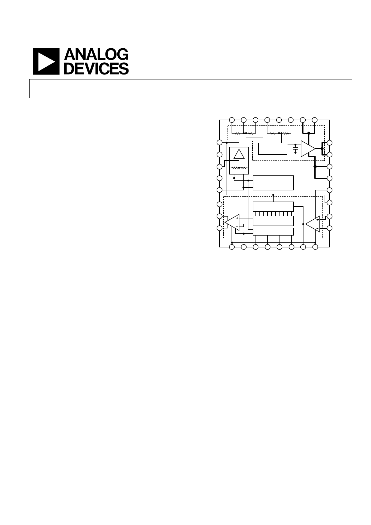
FUNCTIONAL BLOCK DIAGRAM
32
2
3
6
31 30
1.5k 1k
29 28 27 26 25
1k 1.5k
GM
HIGH CURRENT DRIVE R
9
24
23
22
21
VMID
4
1
AD8260
VMDO
TXEN
VMDI
VNCM
VPSB
ENBL
VGAP
VGAN
VNGR VPSR GNS3 GNS2 GNS1 GNS0 PRAO VNGR
V
OCM INPP INRP INRN INPN T XFBVNEGVNEG
TXOP
TXOP
VPOS
VPOS
VPSR
VMDO
PRAI
FDBK
07192-001
5
7
8
10 11 12 13 14 1615
17
18
19
20
BIAS
VGA/PREAMPLIFIER
ATTENUATOR
GM STAGES
LOGIC
×1
+–
Figure 1. Functional Block Diagram
GENERAL DESCRIPTION
The AD8260 includes a high current driver, usable as a
transmitter, and a low noise digitally programmable variable
gain amplifier (DGA), useable as a receiver.
The receiver section consists of a single-ended input preamplifier, and linear-in-dB, differential-output DGA. The receiver has
a small signal –3 dB bandwidth of 230 MHz; the driver small
signal bandwidth is 195 MHz. The driver delivers ±300 mA,
well suited for driving low impedance loads, even when
connected to a 3.3 V supply.
The AD8260 DGA is ideal for trim applications and has a gain
span of 30 dB, in 3 dB steps. Excellent bandwidth uniformity is
maintained across the entire frequency range. The low outputreferred noise of the DGA is advantageous in driving high
speed ADCs. The differential output facilitates the interface to
modern low voltage high speed ADCs.
Single-supply and dual-supply operation makes the part versatile
and enables gain control of negative-going pulses, such as those
generated by photodiodes or photo-multiplier tubes, as well as
processing band-pass signals on a single supply. For maximum
dynamic range, it is essential that the part be ac-coupled when
operating on a single supply.
The AD8260 preamplifier (PrA) is configured with external
resistors for gains greater than 6 dB and can be inverting or
noninverting. The DGA is characterized with a noninverting
preamplifier gain of 2×. The attenuator has a range of 30 dB and
the output amplifier has a gain of 8× (18.06 dB). The lowest
noninverting gain range is −6 dB to +24 dB and shifts up with
increased preamplifier gain. The gain is controlled via a parallel
port (Pin GNS0 to Pin GNS3) with 10 gain steps of 3 dB per
code. The preamplifier and DGA are disabled for any code that
is not assigned a gain step.
The AD8260 can operate with single or dual supplies from 3.3 V
to ±5 V. An internal buffer normally provides a split supply
reference for single-supply operation; an external reference
can also be used when the VMID buffer is shut down.
The operating temperature range is −40°C to +105°C. The
AD8260 is available in a 5 mm × 5 mm, 32-lead LFCSP.
Page 2

AD8260
Rev. 0 | Page 2 of 32
TABLE OF CONTENTS
Features .............................................................................................. 1
Applications ....................................................................................... 1
Functional Block Diagram .............................................................. 1
General Description ......................................................................... 1
Revision History ............................................................................... 2
Specifications ..................................................................................... 3
Absolute Maximum Ratings ............................................................ 6
ESD Caution .................................................................................. 6
Pin Configuration and Function Descriptions ............................. 7
Typical Performance Characteristics ............................................. 8
Test Circuits ..................................................................................... 16
Theory of Operation ...................................................................... 20
Overview ...................................................................................... 20
High Current Driver Amplifier ................................................ 21
Precautions to Be Observed During Half-Duplex
Operation ..................................................................................... 22
VMID Buffer ............................................................................... 22
Preamplifier ................................................................................. 22
Preamplifier Noise ...................................................................... 22
DGA ............................................................................................. 23
Gain Control ............................................................................... 23
Output Stage ................................................................................ 23
Attenuator.................................................................................... 23
Single-Supply Operation and AC Coupling ........................... 24
Power-Up/Power-Down Sequence .......................................... 24
Logic Interfaces ........................................................................... 24
Applications Information .............................................................. 25
Evaluation Board ............................................................................ 26
Connecting the Evaluation Board ............................................ 27
Outline Dimensions ....................................................................... 32
Ordering Guide .......................................................................... 32
REVISION HISTORY
5/08—Revision 0: Initial Version
Page 3
AD8260
Rev. 0 | Page 3 of 32
SPECIFICATIONS
VS (supply voltage) = 3.3 V, TA = 25°C, preamplifier gain = 2× (R
FB1
= R
FB2
= 100 Ω), V
VMDO
= VS/2, f = 10 MHz, CL = 5 pF, R
LOAD
= 500 Ω,
DGA differential output. All dBm values are referenced to 50 Ω, gain code 1011, unless otherwise specified.
Table 1.
Parameter Conditions Min Typ Max Unit
DRIVER AMPLIFIER—GENERAL PARAMETERS
–3 dB Small Signal Bandwidth V
OUT
= 10 mV p-p, R
LOAD
= 500 Ω 195 MHz
V
OUT
= 10 mV p-p, R
LOAD
= 50 Ω 120 MHz
V
OUT
= 10 mV p-p, R
LOAD
= 10 Ω 85 MHz
–3 dB Large Signal Bandwidth V
OUT
= 1 V p-p 195 MHz
V
OUT
= 2 V p-p 190 MHz
V
OUT
= 2 V p-p, R
LOAD
= 50 Ω 180 MHz
Slew Rate V
OUT
= 1 V p-p 730 V/µs
V
OUT
= 2 V p-p 725 V/µs
V
OUT
= 2 V p-p, R
LOAD
= 50 Ω 620 V/µs
Gain Nominal gain with internal gain setting resistors 3.0 3.52 dB
Input Voltage Noise f = 10 MHz 9.5 nV/√Hz
Noise Figure RS = 100 Ω (differential, 2 × 50 Ω that convert
differential DAC output currents to differential voltage)
17.6 dB
Output-Referred Noise Gain = 3.52 dB (1.5×), includes internal gain setting
resistors
14.3 nV/√Hz
Output Impedance DC to 10 MHz, VS = ±3.3 V ≤1.7 Ω
Output Current R
LOAD
= 1 Ω, VIN = ±0.5 V ±310 mA
Output Signal Range R
LOAD
≥ 500 Ω V
MDO
± 1.5 V
V
S
= +5 V V
MDO
± 2.3 V
V
S
= ±5 V
±4.7 V
Input Signal Range Differential input signal 2 V p-p
Output Offset Voltage Gain = 3.52 dB (1.5×), max and min limits are 3σ −20 ±5 +20 mV
DRIVER AMPLIFIER—DYNAMIC PERFORMANCE
Harmonic Distortion V
OUT
= 1 V p-p
HD2 f = 1 MHz −84 dBc
HD3 −85 dBc
HD2 f = 10 MHz −83 dBc
HD3 −70 dBc
Harmonic Distortion V
OUT
= 2 V p-p
HD2 f = 1 MHz −78 dBc
HD3 −76 dBc
HD2 f = 10 MHz −70 dBc
HD3 −58 dBc
Input 1 dB Compression Point 13 dBm
Multitone Power Ratio (MTPR, In-Band) R
LOAD
= 50 Ω, V
OUT
= 1.4 V p-p max, 10 tones, 2 MHz to
22 MHz with missing tone at 12 MHz (spacing 2 MHz)
−49 dBc
R
LOAD
= 50 Ω, V
OUT
= 1.4 V p-p max, 16 tones, 2 MHz to
38 MHz with missing tones at 10 MHz, 20 MHz, 30 MHz,
and 40 MHz (spacing 2 MHz)
−43 dBc
Two-Tone Intermodulation Distortion (IMD3) V
OUT
= 1 V p-p, f1 = 10 MHz, f2 = 11 MHz −90 dBc
V
OUT
= 2 V p-p, f1 = 10 MHz, f2 = 11 MHz −71 dBc
V
OUT
= 1 V p-p, f1 = 45 MHz, f2 = 46 MHz −60 dBc
V
OUT
= 2 V p-p, f1 = 45 MHz, f2 = 46 MHz −48 dBc
Output Third-Order Intercept V
OUT
= 1 V p-p, f = 10 MHz 43 dBm
V
OUT
= 2 V p-p, f = 10 MHz 40 dBm
V
OUT
= 1 V p-p, f = 45 MHz 28 dBm
V
OUT
= 2 V p-p, f = 45 MHz 28 dBm
Two-Tone Intermodulation Distortion (IMD3),
R
LOAD
= 50 Ω
V
OUT
= 1 V p-p, f1 = 10 MHz, f2 = 11 MHz −69 dBc
V
OUT
= 2 V p-p, f1 = 10 MHz, f2 = 11 MHz −72 dBc
V
OUT
= 1 V p-p, f1 = 45 MHz, f2 = 46 MHz −51 dBc
V
OUT
= 2 V p-p, f1 = 45 MHz, f2 = 46 MHz −48 dBc
Page 4
AD8260
Rev. 0 | Page 4 of 32
Parameter Conditions Min Typ Max Unit
Output Third-Order Intercept, R
LOAD
= 50 Ω V
OUT
= 1 V p-p, f = 10 MHz 33 dBm
V
OUT
= 2 V p-p, f = 10 MHz 40 dBm
V
OUT
= 1 V p-p, f = 45 MHz 23 dBm
V
OUT
= 2 V p-p, f = 45 MHz 28 dBm
PREAMPLFIER AND VGA—GENERAL PARAMETERS
−3 dB Small Signal Bandwidth V
OUT
= 10 mV p-p, gain code = 0110 230 MHz
−3 dB Large Signal Bandwidth V
OUT
= 1 V p-p, gain code = 0110 165 MHz
V
OUT
= 2 V p-p, gain code = 0110 135 MHz
Slew Rate V
OUT
= 1 V p-p, gain code = 0110 330 V/µs
V
OUT
= 1.6 V p-p, gain code = 0110 335 V/µs
Input Voltage Noise f = 10 MHz (shorted input) 2.4 nV/√Hz
f = 10 MHz (input open) 6.2 nV/√Hz
Noise Figure Max gain (gain code = 1011), RS = 50 Ω, unterminated 10.2 dB
Max gain (gain code = 1011), RS = 50 Ω,
shunt terminated with 50 Ω
15.5 dB
Output-Referred Noise Max gain (gain code = 1011), gain = 24 dB (input short) 38 nV/√Hz
Max gain (gain code = 1011), gain = 24 dB (input open) 98.1 nV/√Hz
Min gain (gain code = 0001), gain = −6 dB 25 nV/√Hz
Output Impedance DC to 10 MHz ≤3 Ω
Output Signal Range (per Pin) R
LOAD
≥ 500 Ω V
MDO
± 0.7 V
V
S
= +5 V V
MDO
± 1.4 V
V
S
= ±5 V ±3.6 V
Input Signal Range Preamplifier input V
MDO
± 0.3 V
Output Offset Voltage Max gain (gain code = 1011), gain = 24 dB, 3 σ limits −50 ±20 +50 mV
PREAMPLIFIER AND VGA—DYNAMIC PERFORMANCE
Harmonic Distortion Gain code = 0110, gain = 9 dB, V
OUT
= 1 V p-p
HD2 f = 1 MHz −90 dBc
HD3 −87 dBc
HD2 f = 10 MHz −75 dBc
HD3 −58 dBc
Harmonic Distortion Gain code = 1011, gain = 24 dB, V
OUT
= 2 V p-p
HD2 f = 1 MHz −94 dBc
HD3 −90 dBc
HD2 f = 10 MHz −61 dBc
HD3 −84 dBc
Input 1 dB Compression Point Min gain (gain code = 0001), gain = −6 dB
(preamplifier limited)
1.9 dBm
Max gain (gain code = 1011), gain = 24 dB
(VGA limited)
−9.2 dBm
MTPR (In-Band) V
OUT
= 1.4 V p-p-max, 10 tones, 2 MHz to 22 MHz with
missing tone at 12 MHz (spacing 2 MHz),
gain code = 1011, gain = 24 dB
−68 dBc
V
OUT
= 1.4 V p-p-max, 16 tones, 2 MHz to 38 MHz with
missing tones at 10 MHz, 20 MHz, 30 MHz, and 40 MHz
(spacing 2 MHz)
−61 dBc
Two-Tone Intermodulation Distortion (IMD3) Gain code = 1011, gain = 24 dB
V
OUT
= 1 V p-p, f1 = 10 MHz, f2 = 11 MHz −92 dBc
V
OUT
= 2 V p-p, f1 = 10 MHz, f2 = 11 MHz −77 dBc
V
OUT
= 1 V p-p, f1 = 45 MHz, f2 = 46 MHz −50 dBc
V
OUT
= 2 V p-p, f1 = 45 MHz, f2 = 46 MHz −36 dBc
Output Third-Order Intercept Gain code = 1011, gain = 24 dB
V
OUT
= 1 V p-p, f = 10 MHz 44 dBm
V
OUT
= 2 V p-p, f = 10 MHz 43 dBm
V
OUT
= 1 V p-p, f = 45 MHz 27 dBm
V
OUT
= 2 V p-p, f = 45 MHz 22 dBm
Overload Recovery Max gain (gain code = 1011), gain = 24 dB,
V
IN
= 50 mV p-p to 500 mV p-p
50 ns
Group Delay Variation 1 MHz < f < 50 MHz, full gain range 2 ns
Page 5

AD8260
Rev. 0 | Page 5 of 32
Parameter Conditions Min Typ Max Unit
ACCURACY
Absolute Gain Error All gain codes, limits are 3σ −0.5 ±0.15 +0.5 dB
Gain Law Conformance (DNL) Differential gain error code-to-code −0.3 ±0.15 +0.3 dB
GAIN CONTROL
Gain Step per Code 3.0 dB
Gain Range Default = −6dB to +24 dB 30 dB
Resp onse Tim e 30 dB gain change (gain code stepped from 0001 to 1011) 50 ns
LOGIC INTERFACES
High Level Input Voltage 1.4 V
S
V
Low Level Input Voltage 0 0.8 V
Logic Input Bias Current Logic high, V
LOGIC
= 3.3 V 0.2 A
Logic low 18 nA
POWER SUPPLY
Supply Voltage Single supply 3.3 10 V
Dual supply ±3.3 ±5 V
Quiescen t Curren t Full chip enabled (TXEN = 1, ENBL = 1, gain code = 0001) 28.3 mA
TXEN = 0, ENBL = 1, gain code = 0001, driver off, DGA on 19.1 mA
TXEN = 1, ENBL = 1, gain code = 0000, driver on, DGA off 10.8 mA
Chip disabled (TXEN = 0, ENBL = 0, gain code = 0000) 35 µA
V
S
= ±5 V, no signal 34.2 mA
PSRR Max gain (gain code = 1011), gain = 24 dB, 1 MHz −30 dB
Driver amplifier, 1 MHz −48 dB
Power Dissipation No signal 93 mW
No signal, V
POS
− V
NEG
= 10 V 342 mW
ENABLE TIMES
Chip Enable Time Bias only, TXEN = 0, gain code = 0000, ENBL = 0 to 1 0.4 µs
All at once, TXEN = 0 to 1, gain code = 0000 to 0001,
ENBL = 0 to 1
0.3 µs
Preamplifier and DGA Enable Time ENBL = 1, TXEN = 0, gain code = 0000 to 0001 0.3 µs
Driver Enable Time ENBL = 1, gain code = 0001, TXEN stepped from 0 to 1 0.2 µs
DISABLE TIMES
Chip Disable Time TXEN = 1 to 0, gain code = 0001 to 0000,
ENBL = 1 to 0, I
SUPPLY
= 100 A
20 µs
All at once, TXEN = 1 to 0, gain code = 0001 to 0000,
ENBL = 1 to 0, I
SUPPLY
= 35 µA
50 µs
Preamplifier and DGA Disable Time ENBL = 1, TXEN = 0, gain code = 0001 to 0000 0.4 µs
Driver Disable Time ENBL = 1, gain code = 0000, TXEN = 1 to 0 2.2 µs
Page 6
AD8260
Rev. 0 | Page 6 of 32
ABSOLUTE MAXIMUM RATINGS
Table 2.
Parameter Rating
Voltage
Supply Voltage (VPOS, VNEG) ±6 V
Input Voltage (INxx, PRAI,
FDBK, VMDI, VOCM)
VPOS, VNEG
Logic Voltages VPOS, ground
Temperature
Operating Temperature Range –40°C to +105°C
Storage Temperature Range –65°C to +150°C
Lead Temperature (Soldering, 60 sec) 300°C
Thermal Data1
Maximum Junction Temperature 125°C
θJA 47.3°C/W
θJC 6.9°C/W
θJB 28.6°C/W
ΨJT 0.6°C/W
ΨJB 27.4°C/W
1
Thermal data at zero airflow with exposed pad soldered to four-layer JEDEC
board with vias per JESD51-5.
Stresses above those listed under Absolute Maximum Ratings
may cause permanent damage to the device. This is a stress
rating only; functional operation of the device at these or any
other conditions above those indicated in the operational
section of this specification is not implied. Exposure to absolute
maximum rating conditions for extended periods may affect
device reliability.
ESD CAUTION
Page 7
AD8260
Rev. 0 | Page 7 of 32
PIN CONFIGURATION AND FUNCTION DESCRIPTIONS
7192-002
8
7
6
5
1
4
3
2
29303132 28 252627
20
17
18
19
21
22
23
24
VPSR
FDBK
PRAI
VMDO
VPOS
VPOS
TXOP
TXOP
INPN
VNEG
VNEG
TXFB
INRN
INRP
INPP
VOCM
14139121110 15 16
PIN 1
INDICATOR
AD8260
TOP VIEW
(Not to Scale)
VMDO
TXEN
VMDI
VNCM
VPSB
ENBL
VGAP
VGAN
VNGR
VPSR
GNS3
GNS2
GNS1
GNS0
PRAO
VNGR
Figure 2. Pin Configuration
Table 3. Pin Function Descriptions
Pin No. Mnemonic Description
1, 191 VMDO VMID Buffer Output. Requires robust ac decoupling with a capacitance of 0.1 µF capacitor or greater.
2 TXEN Driver Enable. Logic threshold = 1.1 V with ±0.2 V hysteresis.
3 VMDI
VMID Input Voltage. Normally decoupled with a 0.1 µF capacitor. When pulled to VNCM, the VMID buffer shuts
down. This can be useful when using the part with dual supplies or when an external midpoint generator is used.
4 VNCM Negative Supply for Bias Cell, VMID Cell, and Logic Inputs. (Ground this pin in applications.)
5 VPSB Positive Supply for Bias Cell and VMID Cell.
6 ENBL
Enable. Logic threshold = 1.1 V. When low, the AD8260 is disabled and the supply current is 35 µA when TXEN
and all GNSx pins are also low.
7 VGAP Positive VGA Output (Needs to Be Ac-Coupled for Single Supply).
8 VGAN Negative VGA Output (Needs to Be Ac-Coupled for Single Supply).
9, 161 VNGR Negative Supply for Preamplifier and DGA (Set to −VPOS for Dual Supply; GND for Single Supply).
10, 201 VPSR Positive Supply for Preamplifier, DGA, and GNSx Logic Decoder.
11 GNS3 MSB for Gain Control. Logic threshold = 1.1 V.
12 GNS2 Gain Control Bit. Logic threshold = 1.1 V.
13 GNS1 Gain Control Bit. Logic threshold = 1.1 V.
14 GNS0 LSB for Gain Control. Logic threshold = 1.1 V.
15 PRAO Preamplifier Output.
17 FDBK Negative Input of Preamplifier.
18 PRAI Positive Input of Preamplifier.
21, 221 VPOS Positive Supply for Driver Amplifier.
23, 241 TXOP Driver Output.
25, 261 VNEG Negative Supply for Driver Amplifier (Set to −VPOS for Dual Supply; GND for Single Supply).
27 TXFB Feedback for Driver Amplifier.
28 INPN Negative Driver Amplifier Input.
29 INRN Negative Gain Resistor Input for Driver Amplifier.
30 INRP Positive Gain Resistor Input for Driver Amplifier.
31 INPP Positive Driver Amplifier Input.
32 VOCM Output Common Mode Pin. Normally connected to Pin VMDO.
1
Pins with the same name are connected internally.
Page 8
AD8260
Rev. 0 | Page 8 of 32
TYPICAL PERFORMANCE CHARACTERISTICS
VS (supply voltage) = 3.3 V, TA = 25°C, CL = 5 pF, f = 10 MHz, preamplifier gain = 2×, R
FB1
and R
FB2
of the preamplifier = 100 ,
R
LOAD
of the driver amplifier = 500 , TX and RX enabled, unless otherwise specified.
5
1
0
2
3
4
GAIN (dB)
FREQUENCY (Hz)
200M
100M
10M1M100k
T = –40°C
V
OUT
= 200 mV p -p
T = +105° C
07192-003
T= +25°C
Figure 3. Small-Signal Frequency Response at Three Temperatures of the
High Current Driver—See Figure 51
5
1
0
2
3
4
GAIN (dB)
FREQUENCY (Hz)
200M
100M
10M1M100k
VS = +5V
V
OUT
= 200 mV p -p
VS = +3.3V
VS = ±5V
07192-004
Figure 4. Small-Signal Frequency Response of the High Current Driver for
Three Supply Voltages—See Figure 51
5
1
0
2
3
4
GAIN (dB)
FREQUENCY (Hz)
200M
100M
10M1M100k
07192-005
V
LOAD
= 1V p-p; R
LOAD
=50
V
LOAD
= 1V p-p; R
LOAD
=500
V
LOAD
= 2V p-p; R
LOAD
=50
V
LOAD
= 2V p-p; R
LOAD
=500
Figure 5. Large-Signal Frequency Response of the High Current Driver for Two
Values of Output Voltage and Two Values of Load Resistance—See Fig ure 51
20
0
5
10
15
NOISE (nV/Hz)
FREQUENCY (Hz)
50M10M1M100k
RTO
RTI
07192-006
Figure 6. Input-Referred and Output-Referred Noise of the High Current
Driver—See Figure 52
10
OUTPUT IMP EDANCE ()
FREQUENCY (Hz)
100M10M1M100k
100
0.1
1
7192-007
Figure 7. Output Impedance of the High Current Driver
See Figure 53
– 100
HARMONIC DIST ORTION ( dBc)
LOAD RESISTANCE ()
1k10010
–40
–
20
–60
–80
–90
HD3
HD2
–70
–50
–30
2V p-p
1V p-p
07192-008
Figure 8. Harmonic Distortion (HD2, HD3) vs. Load Resistance for the High
Current Driver—See Figure 54
Page 9
AD8260
Rev. 0 | Page 9 of 32
–100
HARMONIC DISTORTION (d Bc)
LOAD CAPACITANCE ( pF)
100400
–40
–
20
–60
–80
–90
802010 60
f = 10MHz
–70
–50
–30
50 9030 70
HD2, V
OUT
= 1V p-p
HD3, V
OUT
= 1V p-p
HD2, V
OUT
= 2V p-p
HD3, V
OUT
= 2V p-p
07192-009
Figure 9. Harmonic Distortion (HD2, HD3) vs. Load Capacitance at Two
Values of Output Voltage for the High Current Driver—See Figure 54
–100
HARMONIC DIST ORTION ( dBc)
OUTPUT VOLTAGE (V p-p)
3.01.50
–40
–20
–60
–80
–120
0
2.51.00.5 2.0
HD3
HD2
f = 10MHz
07192-010
Figure 10. Harmonic Distortion (HD2, HD3) vs. Output Voltage for the High
Current Driver—See Figure 54
–100
HARMONIC DISTORTION (d Bc)
FREQUEN CY (Hz)
100M10M
1M
–40
–
20
–60
–80
–90
HD3
HD2
–70
–50
–30
1V p-p
2V p-p
07192-011
Figure 11. Harmonic Distortion (HD2, HD3) vs. Frequency of the High Current
Driver at Two Values of Output Voltage—See Figure 54
100M
FREQUENCY (Hz)
2M
IMD3 (dBc)
10M
–100
–80
–60
–40
–20
0
R
LOAD
= 50, V
OUT
= 1V p-p
R
LOAD
= 50, V
OUT
= 2V p-p
R
LOAD
= 500, V
OUT
= 1V p-p
R
LOAD
= 500, V
OUT
= 2V p-p
07192-012
Figure 12. IMD3 vs. Frequency for Two Values of Output Voltage and Two
Values of Load Resistance for the High Current Driver—See Figure 55
100M
FREQUENCY (Hz)
2M
OIP3 (dBm)
10M
50
40
30
20
10
0
R
LOAD
= 50, V
OUT
= 1V p-p
R
LOAD
= 50, V
OUT
= 2V p-p
R
LOAD
= 500, V
OUT
= 1V p-p
R
LOAD
= 500, V
OUT
= 2V p-p
07192-013
Figure 13. Third-Order Intercept (OIP3) vs. Frequency for the High Current Driver
See Figure 55
0
20
IP1dB (dBm)
FREQUENCY (Hz)
100M10M1M
5
15
10
R
LOAD
= 50
R
LOAD
= 500
07192-014
Figure 14. Input-Referred 1 dB Compression (IP1dB) vs. Frequency for Two
Values of Load Resistance for the High Current Driver
Page 10
AD8260
Rev. 0 | Page 10 of 32
–80
FREQUENCY (MHz)
24221821006124201614
0
8
OUTPUT (d Bm)
–60
–40
–90
–70
–20
–50
–30
–10
07192-015
Figure 15. Missing Tone Power Ratio for the High Current Driver
0
0.15
–0.15
0 .05
0.10
OUTPUT VOL TAGE (V)
TIME (ns)
807060
–0.05
–0.10
–20 10–30 0 30–10 20 5040
–0.20
0.20
R
LOAD
= 10
R
LOAD
= 50
R
LOAD
= 100
R
LOAD
= 500
C
LOAD
= 5pF
NONINVE RTING
07192-016
Figure 16. Small-Signal Pulse Resp onse of the High Current Driver for Various
Values of Load Resistance, R
LOAD
—See Figure 56
0
0.15
–0.15
0.05
0.10
OUTPUT VOLTAGE (V)
TIME (ns)
807060
–0.05
–0.10
–20 10–30 0 30–10 20 5040
–0.20
0.20
C
LOAD
= 5pF
C
LOAD
= 47pF
C
LOAD
= 10pF
R
LOAD
= 500
NONINVERTING
07192-017
Figure 17. Small-Signal Pulse Resp onse of the High Current Driver for Various
Values of Load Capacitance, C
LOAD
, and R
LOAD
= 500 Ω—See Figure 56
0
0.15
–0.15
0.05
0.10
OUTPUT VOLTAGE (V)
TIME (ns)
807060
–0.05
–0.10
–20 10–30 0 30–10 20 5040
–0.20
0.20
C
LOAD
= 5pF
C
LOAD
= 47pF
C
LOAD
= 10pF
R
LOAD
= 50
NONINVERTI NG
07192-018
Figure 18. Small-Signal Pulse Resp onse of the High Current Driver for Various
Values of Load Capacitance, C
LOAD
, and 50 Ω Load—See Figure 56
OUTPUT VOLT AGE (V)
TIME (ns)
80706020 1030 0 3010 20 5040
2.0
1.5
1.0
0.5
0
–0.5
–1.0
–1.5
–2.0
R
LOAD
=10
R
LOAD
= 50
R
LOAD
=100
R
LOAD
= 500
C
LOAD
=5pF
NONINVERTI NG
07192-019
Figure 19. Large-Signal Pulse Response of the High Current Driver for Various
Values of Load Resistance, R
LOAD
—See Figure 56
0
1.5
–1.5
0.5
1.0
OUTPUT VOLTAGE (V)
TIME (ns)
807060
–0.5
–1.0
–20 10–30 0 30–10 20 5040
–2.0
2.0
C
LOAD
= 5pF
C
LOAD
= 47pF
C
LOAD
= 10pF
R
LOAD
= 500
NONINVERTING
07192-020
Figure 20. Large-Signal Pulse Response of the High Current Driver for Various
Values of Load Capacitance, C
LOAD
, and R
LOAD
= 500 Ω—See Figure 56
Page 11

AD8260
Rev. 0 | Page 11 of 32
OUTPUT VOL TAGE (V)
TIME (ns)
C
LOAD
=5pF
C
LOAD
= 10pF
C
LOAD
= 47pF
807060–20 10–30 0 30–10 20 5040
R
LOAD
=50
NONINVERTING
2.0
1.5
1.0
0.5
0
–0.5
–1.0
–1.5
–2.0
07192-021
Figure 21. Large-Signal Pulse Response of the High Current Driver for Various
Values of Load Capacitance, C
LOAD
, and 50 Ω Load—See Figure 56
27
24
21
18
15
12
9
6
3
0
–3
–6
–9
GAIN SELECT CODE
GAIN (dB)
07192-022
10111010100110000111011001010001 010000110010
AVERAGE OF 3 SAMPLES
f = 1MHz, 10MHz, AND 40MHz
Figure 22. Gain vs. Gain Select Code for Three Samples for the
VGA/Preamplifier at Three Frequencies—See Figure 57
4.00
3.75
3.50
3.25
3.00
2.75
2.50
2.25
2.00
GAIN STEP (dB)
07192-023
AVERAGE OF 3 SAMPLES
f = 1MHz, 10MHz, AND 40MHz
GAIN SELECT CODE
1011101010011000011101100101010000110010
Figure 23. Gain Step vs. Gain Select Code for Three Samples for the
VGA/Preamplifier at Three Frequencies—See Figure 57
1.00
0.75
0.50
0.25
0
–0.25
–0.50
–0.75
–1.00
0001 00 10 0011 0100 0101 0110 0111 1000 1001 1010 1011
GAIN SELECT CODE
ABSOLUTE G AIN ERROR (dB)
07192-024
AVERAGE OF 3 SAMPLES
f = 1MHz, 10MHz, AND 40MHz
Figure 24. Absolute Gain Error vs. Gain Select Code for Three Samples for the
VGA/Preamplifier at Three Frequencies Normalized to 1 MHz and Code 0110
See Figure 57
1.00
0.75
0.50
0.25
0
–0.25
–0.50
–0.75
–1.00
0001 0010 0011 0100 01 01 0110 0111 1000 100 1 1010 1011
GAIN SELECT CODE
GAIN ERROR (dB)
07192-025
AVERAGE OF 3 SAMPLESAT
EACH TEMPERATURE
T = +105° C
T = +25° C
T = –40°C
Figure 25. Gain Error vs. Gain Select Code at Three Temperatures for the
VGA/Preamplifier—See Figure 57
0
–40
–30
–20
50
20
30
40
–50
OFFSET VOLTAGE (mV)
GAIN SELECT CODE
1010100110000111011001010001 010000110010
AVERAGE OF 3 SAMP LES AT
EACH TEMPERATURE
1011
10
–10
T = +105° C
T = +25°C
T = –40°C
07192-026
Figure 26. Output Offset Voltage vs. Gain Select Code at Three Temperatures
for the VGA/Preamplifier—See Figure 58
Page 12

AD8260
Rev. 0 | Page 12 of 32
27
24
21
18
15
12
9
6
3
0
–3
–12
–6
–9
100k 1M 10M 100M 200M
FREQUENCY (Hz)
DIFFERENTIAL GAIN (d B)
07192-027
1011
1010
1001
1000
0111
0110
0101
0100
0011
0010
0001
Figure 27. Frequency Response for a Supply Voltage (V
S
) of 3.3 V for all Codes
of the VGA/Preamplifier—See Figure 59
27
24
21
18
15
12
9
6
3
0
–3
–12
–6
–9
100k 1M 10M 100M 200M
FREQUENCY (Hz)
DIFFERENTIAL GAIN (dB)
07192-028
1011
1010
1001
1000
0111
0110
0101
0100
0011
0010
0001
VS = 5V
Figure 28. Frequency Response for a Supply Voltage (VS) of 5 V for All Codes
for the VGA/Preamplifier—See Figure 59
27
24
21
18
15
12
9
6
3
0
–3
–12
–6
–9
100k 1M 10M 100M 200M
FREQUENCY (Hz)
DIFFE RENTI AL GAI N (dB)
07192-029
1011
1010
1001
1000
0111
0110
0101
0100
0011
0010
0001
VS = ±5V
Figure 29. Frequency Response for a Dual Supply (VS) = ±5 V for All Codes for
the VGA/Preamplifier—See Figure 59
10
8
6
4
2
0
1M 10M 100M
FREQUENCY (Hz)
GROUP DELAY (ns)
07192-030
Figure 30. Group Delay vs. Frequency for the VGA/Preamplifier
See Figure 59
100
OUTPUT RESI STANCE ()
FREQUENCY (Hz)
100M
0.1
1M100k 10M
VGAP
10
1
VGAN
7192-031
Figure 31. Output Resistance vs. Frequency for the VGA/Preamplifier
See Figure 60
10
50
20
30
40
GAIN SELECT CODE
OUTPUT-REFERRED NOISE (nV/
Hz)
1010100110000111011001010001 010000110010 1011
07192-032
Figure 32. Output-Referred Noise vs. Gain Select Code for the
VGA/Preamplifier—See Figure 61
Page 13

AD8260
Rev. 0 | Page 13 of 32
10
100
FREQUENCY (Hz)
OUTPUT-REF ERRED NOISE (n V/Hz)
10M10 0k 1M 50M
GAIN CODE = 1011
07192-033
Figure 33. Output-Referred Noise vs. Frequency for the VGA/Preamplifier at
Maximum Gain—See Figure 61
1
100
10
GAIN SELECT CODE
INPUT- REFERR ED NOISE (nV/ Hz)
101010011000011101100101000 1 010000110010 1011
07192-034
Figure 34. Input-Referred Noise vs. Gain Select Code for the VGA/Preamplifier
See Figure 61
1
10
FREQUENCY (Hz)
SHORT-CIRCUIT INPUT-REF ERRED NOISE
(nV/Hz)
10M100k 1M 50M
GAIN CODE = 1011
07192-035
Figure 35. Short-Circuit Input Noise vs. Frequency for the VGA/Preamplifier
See Figure 61
50
HARMONIC DIST ORTION ( dBc)
LOAD RESIST ANCE ()
1800160014001200200 10008004000 2000
30
40
60
80
70
600
HD2
HD3
07192-036
V
OUT
= 1V p-p
GAIN CODE = 0110
Figure 36. Harmonic Distortion (HD2, HD3) vs. Load Resistance for the
VGA/Preamplifier—See Figure 62
LOAD CAPACITANCE (p F)
HARMONIC DIST ORTION ( dBc)
–70
–60
–50
–40
–
30
–80
10 4003020
50
V
OUT
= 1V p-p
GAIN CODE = 0110
HD2
HD3
07192-037
Figure 37. Harmonic Distortion (HD2, HD3) vs. Load Capacitance for the
VGA/Preamplifier—See Figure 62
–120
HARMONIC DISTORTION (d Bc)
GAIN SELECT CODE
101010011000011101100101 1011
–20
–40
–60
–80
–100
0
MEASUREMENT O F
DISTORTION IS
LIMITED BY THE
MAXIMUM DYNAMIC
INPUT RANGE OF
THE PREAMPLIFIER
HD2,
f
C
= 1MHz
V
OUT
= 1V p-p
HD3,
f
C
= 1MHz
HD2,
f
C
= 10MHz
HD3,
f
C
= 10MHz
07192-038
Figure 38. Harmonic Distortion (HD2, HD3) vs. Gain Select Code at 1 MHz
and 10 MHz for the VGA/Preamplifier—See Figure 62
Page 14

AD8260
Rev. 0 | Page 14 of 32
0
–100
HARMONIC DISTORTION (dBc)
FREQUENCY (Hz)
100M10M1M
–40
–20
–60
–80
–120
HD2
HD3
GAIN CODE = 1011
V
OUT
= 1V p-p
07192-039
Figure 39. Harmonic Distortion (HD2, HD3) vs. Frequency for the
VGA/Preamplifier—See Figure 62
0
–100
IMD3 (dBc)
FREQUENCY (Hz)
100M10M1M
–40
–20
–60
–80
–120
LOWER
UPPER
V
OUT
= 1V p-p
TONES 1MHz APART
EACH TONE 0.5V p-p
GAIN CODE = 1011
07192-040
Figure 40. Third-Order Intermodulation Distortion (IMD3) vs. Frequency for
the VGA/Preamplifier
60
10
OIP3 (dBm)
FREQUENCY (Hz)
100M10M1M
40
50
30
20
0
LOWER
UPPER
GAIN CODE = 1011
TONES 1MHz APART
07192-041
Figure 41. OIP3 vs. Frequency for the VGA/Preamplifier
10
5
0
–5
–10
–15
–20
–25
–30
GAIN SELECT CODE
INPUT IP1dB (dBm)
1010100110000111011001010001 010000110010 1011
1MHz
10MHz
IP1dB LIMITED AT LOW GAIN BY THE
DYNAMIC RANGE OF THE PREAMPLI FIER
07192-042
Figure 42. Input 1 dB Compression (IP1dB) vs. Gain Select Code at 1 MHz and
10 MHz for the VGA/Preamplifier
07192-043
CH1 2. 00V
M10.0ns A CH4 180µV
1
M
T 27.2000ns
T
MATH 5.00mV 10.0ns
INPUT
OUTPUT
50mV/DIV
0V
2mV/DIV
0V
Figure 43. Small-Signal Pulse Resp onse for the VGA/Preamplifier
07192-044
CH3 20. 0mV
M10.0ns A CH4 200µV
3
M
T 27.2000ns
T
MATH 50.0mV 10.0ns
INPUT
OUTPUT
500mV/DIV
0V
20mV/DIV
0V
Figure 44. Large-Signal Pulse Response for the VGA/Preamplifier
Page 15

AD8260
Rev. 0 | Page 15 of 32
1.5
1.0
0.5
0
–0.5
–1.0
–1.5
–3–2–1012345678
TIME (ns)
OUTPUT VO LTAGE (V)
07192-045
VS = +3V, +5V, AND ±5V
Figure 45. Large-Signal Pulse Resp onse for Various Values of Supply Voltage
for the VGA/Preamplifier
07192-046
CH1 1.00V CH2 20.0mV
MATH 100mV 200n V
CH2 20.0mV
M200ns A CH1 760mV
1
M
4
T 595.200ns
CH1 AMPL
3.28V
CH2 AMPL
1.20mV
MATH AMPL
117mV
T
Figure 46. Gain Response for the VGA/Preamplifier, Yellow: Gain Code Select,
Red: VGA Differential Output, Blue/Green: VGAP and VGAN
0
1
OUTPUT VOLTAGE (V)
TIME (ns)
800700600
–1
–200 1000 300–100 200 500400
–2
2
07192-047
Figure 47. Overdrive Recovery of the VGA/Preamplifier—Gain Code = 1011
FREQUENCY (Hz)
PSRR (dB)
1M100k 5M
–
10
–20
–30
–40
–50
–60
–70
–SUPPLY HIGH CURRENT DRIVER
+SUPPLY HIG H CURRENT DRIVER
+SUPPLY VGA/PREAMPLIFIER
–SUPPLY VGA PREAMPLIFIER
VS= ±3.3V
GAIN CODE = 1011
07192-048
Figure 48. PSRR vs. Frequency for Dual Supplies for the High Current Driver
and the VGA/Preamplifier
QUIESCENT S UPPLY CURRENT (mA)
0
40
30
–55
10
TEMPERATURE (
°
C)
525452065 85 105 125
–15–35
5
15
35
25
FULLY ENABLE D
VGA/PREAMPLIFIER ENABLED
HIGH CURRENT DRIVE R ENABLED
07192-049
Figure 49. Quiescent Supply Current vs. Temperature for Three Operating States
STANDBY QUIESCE NT SUPPLY CURRENT (µA)
–55 –35 –15
TEMPERATURE (° C)
5 25 45 65 85 105 125
80
70
60
50
40
30
20
10
0
07192-050
Figure 50. Standby Quiescent Supply Current vs. Temperature
Page 16

AD8260
Rev. 0 | Page 16 of 32
TEST CIRCUITS
INRP
–
+
NETWORK ANALYZ ER
VOCM
453
INRN
50
INOUT
0.1µF
5pF
0.1µF
50
AD8260—HIGH CURRENT DRI VER
TXFB
TXOP
VMDO
50
0.1µF
+
–
07192-151
Figure 51. Test Circuit for Frequency Response of the High Current Driver
IN
50
INRP
–
+
VOCM
INRN
0
.1µ
F
0
.1µ
F
0.1µF
TXFB
TXOP
–
+
VMDO
SPECTRUM
ANALYZER
07192-152
AD8260—HIGH CURRENT DRIVER
Figure 52. Test Circuit for Input-Referred and Output-Referred Noise of the High Current Driver
NETWORK ANALYZ ER
WITH S-PARAMETER MODE
IN
50
INRP
VOCM
INRN
0.1µF
0.1µF
TXFB
TXOP
+3.3
V
–3.3V
–
+
07192-153
AD8260—HIGH
CURRENT DRIVER
Figure 53. Test Circuit for Output Impedance of the High Current Driver
SIGNAL
GENERATOR
50
LP
FILTER
IN
50
INRP
VOCM
INRN
0.1µF
0.1µF
0.1µF
TXFB
TXOP
VMDO
SPECTRUM
ANALYZER
50
50
R
LOAD
C
LOAD
1:1
07192-154
AD8260—HIGH CURRENT DRI VER
–
+
Figure 54. Test Circuit for Harmonic Distortion of the High Current D river
Page 17

AD8260
Rev. 0 | Page 17 of 32
SIGNAL
GENERATORS
50
IN
50
INRP
VOCM
INRN
0.1µF
0.1µF
0.1µF
TXFB
TXOP
VMDO
SPECTRUM
ANALYZER
453
1k
1k
1:1
07192-155
AD8260—HIGH CURRENT DRI VER
50
–
+
Figure 55. Test Circuit for IMD3 and OIP3 of the High Current Driver
OSCILLOSCOPE
IN
50
50
INRP
–
+
VOCM
INRN
0.1µF
0.1µF
0.1µF
TXFB
TXOP
VMDO
50
12.5
R
LOAD
C
LOAD
07192-156
AD8260—HIGH CURRENT DRI VE
R
Figure 56. Test Circuit for Pulse Response of the High Current Driver
OSCILLOSCOPE
IN 50
50
453
453
VMDO
0.1µF
0.1µF
0.1µF
100
SIGNAL
GENERATOR
50
+
–
100
PREAMP
07192-157
AD8260—VGA/PREAM PLIFI E
R
Figure 57. Test Circuit for Gain Step Size and Error of the VGA/Preamplifier
DMM
VMDO
0.1µF
100
+
–
100
PREAMP
07192-158
AD8260—VGA/PREAM PLIFI E
R
Figure 58. Test Circuit for Output-Referred Offset Voltage of the VGA/Preamplifier
Page 18

AD8260
Rev. 0 | Page 18 of 32
VMDO
0.1µF
100
+
–
100
PREAMP
IN
NETWORK ANALYZ ER
0.1µF
453
0.1µF
453
50
50
07192-159
AD8260—VGA/PREAM PLIFI ER
Figure 59. Test Circuit for Frequency Response and Group Delay of the VGA/Preamplifier
+3.3V
–3.3V
0.1 µF
100
+
–
100
PREAMP
IN
NETWORK ANALY ZE
R
WITH S-PARAM ETER
CAPABILITY
50
07192-160
AD8260—VGA/
PREAMPLIFIER
Figure 60. Test Circuit for Output Resistance of the VGA/Preamplifier
0.1µF
1k
1k
100
100
VMDO
VMDO
SPECTRUM
ANALYZER
50
+
–
PREAMP
VGA
0.1µF
0.1µF
0.1µF
AD8129
×10
07192-051
AD8260—VGA/PRE AMPLIF IER
Figure 61. Test Circuit for Input-Referred and Output-Referred Noise Measurements of the VGA/Preamplifier
Page 19

AD8260
Rev. 0 | Page 19 of 32
0.1µF
475
475
100
100
VMDO
+
–
PREAMP
0.1µF
0.1µF
07192-052
SPECTRUM
ANALYZER
50
1:1
LP
FILTER
50
50
SIGNAL
GENERATOR
IN
AD8260—VGA/PREAM PLIFI ER
Figure 62. Test Circuit for Harmonic Distortion Measurements of the VGA/Preamplifier
VMDO
0.1µF
100
+
–
100
PREAMP
OSCILLOSCOPE
50
50
IN 50
07192-163
A
D8260—VGA/PRE AMPLIF IE
R
Figure 63. Test Circuit for IP1dB, Pulse Response, Overdrive Recovery, and Gain Response of the VGA/Preamplifier
Page 20

AD8260
Rev. 0 | Page 20 of 32
THEORY OF OPERATION
OVERVIEW
The AD8260 is a self-contained transceiver intended for analog
communications using a power line as the media. Operating on
supplies as low as 3.3 V, it includes a high current driver usable
as a transmitter and a low noise digitally programmable variable
gain amplifier (DGA), usable as a receiver (see Figure 64). An
uncommitted current-feedback high frequency op amp acts as a
preamplifier and interface to the DGA and is user configured
for gains greater than 6 dB. Combined, the VGA and preamplifier
are usable at high signal levels from dc to 100 MHz, with a
small-signal −3 dB bandwidth of 230 MHz. To implement a
high current-output VGA, the VGA output can be connected
to the driver-amplifier differential input.
The small-signal −3 dB bandwidth of the driver amplifier is
195 MHz and the large-signal bandwidth is >115 MHz, even
when driving a 50 load.
The device is fabricated on the Analog Devices, Inc., high speed
(eXtra Fast Complementary Bipolar) XFCB process. The preamplifier and DGA feature low dc offset voltage, and a nominal
gain range of −6 dB to +24 dB, a 30 dB gain span, and a differential
output for ADC driving. The power consumption is 93 mW
with a single 3.3 V supply. The supply current is typically about
28 mA when all circuits in the device are active. During normal
usage, either the driver amplifier is on or the preamplifier and
DGA are on and, therefore, the supply current in general is less
than 28 mA. The gain of the AD8260 VGA is programmed via a
4-bit parallel interface. Figure 64 shows the circuit block
diagram and basic application connections, and illustrates the
envisioned external DAC, ADC, and power-line bus interface
connections. The diagram shows the connections for single 3.3 V
supply operation; if a dual supply is available, the VMID
generator can be shut down and Pin VMDI, Pin VMDO, and
Pin VOCM need to be grounded. Note that Pin VNCM
functions as the negative supply for the bias and VMID cells,
plus the logic interfaces, and should always be tied to ground.
For optimal dynamic range, it is important that the inputs and
outputs to both the driver amplifier and the preamplifier and
the DGA output amplifier be ac-coupled in a single-supply
application. In Figure 64, the DAC and ADC are presumed to
operate on a 1.8 V or 3.3 V supply with a corresponding limited
output and input swing. The DAC outputs are currents that
point down and generate a voltage in the 50 resistors that are
connected to ground. The maximum voltage with a peak DAC
output current of 15 mA is 0.75 V; if a DAC with a 20 mA peak
current is used, then the maximum voltage is 1 V per side for a
differential input signal of 2 V p-p.
The driver amplifier supports a 3 V p-p output swing on a
3.3 V supply. Because of its gain of 1.5, the maximum input
swing is 2 V p-p. The corresponding maximum output swing for
the DGA is 2.4 V p-p differential; the input to the preamplifier
can be a maximum of 0.6 V p-p.
Page 21

AD8260
Rev. 0 | Page 21 of 32
32
2
3
6
31 30
1.5k 1k
29 27 26 25
1k 1.5k
GM
9
24
23
22
21
VMID
4
×1
1
AD8260
VMDO
TXEN
VMDI
VNCM
VPSB
ENBL
VGAP
VGAN
VNGR
VPSR
GNS3
GNS2
GNS1
GNS0
PRAO
VNGR
VOCM INPP
INRP
INRN
INPN
TXFB
VNEG
VNEG
TXOP
TXOP
VPOS
VPOS
VPSR
VMDO
PRAI
FDBK
07192-053
50
0.1µF
0.1µF
0V, 1.8V/ 3.3V
0V, 1.8V/3.3V
5
3.3V
7
8
0.1µF
0.1µF
1.8V OR 3.3V
ADC
FS INPUT
2V p-p
INP
INN
10
3.3V
11 12 13 14 1615
17
18
19
RFB1
100
RFB2
100
0.1µF
20
3.3V
0.1µF
0.1µF
POWERLINE
CABLE, ETC.
OPTIO NAL CLAMP DIO DES
AND SNUBBING RESIST ORS
0.1µF0.1µF
50
1.8V OR 3.3V
20mA DAC
1V MAX WITH
200mA pk
BIAS
ATTENUATOR
GM STAGES
LOGIC
28
C
FB
OPTIONAL USER SELECTED
C
FB
REDUCES HF PEAKING
WITH CAPACIT IVE LOADING
LOW-PASS
AA FILTER
+–
Figure 64. Block Diagram and Basic Application Connections
HIGH CURRENT DRIVER AMPLIFIER
The high current driver amplifier can deliver very large output
currents suitable for driving complex impedances, such as a
power line, a 50 line, or a coaxial cable. The input of the
amplifier is fully differential and intended to be driven by a
differential current-output DAC, as shown in Figure 64. The
differential input signal is amplified by 1.5× and produces a
2.25 V p-p single-ended output signal from a 1.5 V p-p input
signal. A DAC with 15 mA maximum output current into a
50 Ω load provides 1.5 V p-p of input voltage and results in
2.25 V p-p at the output. A DAC whose output is 20 mA produces
an output swing of 3 V p-p (neglecting a small gain error when
driving the parallel combination of the 50 Ω load-resistor and the
internal 1 kΩ gain resistor of the AD8260).
For a 3.3 V supply rail, the maximum limit of the output voltage
is 3 V p-p and distorts severely if exceeded. The recommended
output for optimum distortion is 2 V p-p for a 3.3 V supply.
Correspondingly, larger output swings are accommodated for
higher supply voltages such as +5 V or ±5 V.
For optimum distortion, the input drive must be controlled
such that the output swing is well within saturation levels
established by the supply rail. The output swing can be reduced
by using load resistors with values less than 50 or by reducing
the amplifier gain by connecting external resistors in parallel
with the internal 1 kΩ and 1.5 kΩ resistors between Pin 27,
Pin 28, and Pin 29, and between Pin 30, Pin 31, and Pin 32.
Coincidently, noise is reduced because the gain setting resistors
are the primary noise sources of the high current driver amplifier.
The output-referred noise is 14 nV/√Hz, of which 11 nV/√Hz is
due to the gain setting resistors. Matching of the gain setting
resistors is important for good common-mode rejection and the
accuracy of the differential gain. If external resistors are used,
their accuracy should be at least ±1%. How low the resistor
values can be is primarily determined by the quality of the ac
ground at Pin VOCM; as the gain setting resistors decrease in
value, the dynamic current increases, and the quality of the
decoupling capacitors needs to increase correspondingly.
Page 22

AD8260
Rev. 0 | Page 22 of 32
PRECAUTIONS TO BE OBSERVED DURING HALFDUPLEX OPERATION
During receive, when the high current driver-amplifier is
disabled, its gain setting resistors provide a signal path from
input to output. To prevent inadvertent DAC signals from being
transmitted while receiving via the preamplifier and DGA, the
DAC in Figure 64 must have no output signal.
During transmit, the preamplifier and VGA should be disabled
through any of the nongain-setting codes (see Table 4).
VMID BUFFER
The VMID buffer is a dc bias source that generates the voltage
on Pin 1 and Pin 19, VMDO. Node VMDO cannot accommodate
large dynamic currents and requires excellent ac decoupling to
ground. A high quality 0.1F capacitor located as close as
possible to Pin 1 and Pin 19 (see Figure 64) is normally sufficient
to decouple the high values of current from Node VMDO.
When operating with dual power supplies, the buffer is disabled
by connecting Pin VMDI, Pin VOCM, and Pin VMDO to ground.
Because the logic decoder in the DGA (GNSx inputs) requires
3.3 V of headroom, the positive supply rails must be 3.3 V or
greater whether single-ended or dual. If a dual supply is used,
the negative rails are the same magnitude (opposite polarity)
as the positive, that is, −3.3 V when VPOS, VPSB, and VPSR
are +3.3 V.
PREAMPLIFIER
The AD8260 includes an uncommitted current feedback op
amp to buffer the resistive attenuator of the DGA. External
resistors are used to adjust the gain. The preamplifier is
characterized with a noninverting gain of 6 dB (2×) and both
gain resistor values of 100 Ω. The preamplifier gain can be
increased using different gain ratios of R
FB1
and R
FB2
, trading off
bandwidth and offset voltage. The sum of the values of R
FB1
and
R
FB2
should be ≥200 Ω to maintain low distortion. R
FB2
should
be ≥100 Ω because it and an internal compensation capacitor
determine the −3 dB bandwidth of the amplifier. Smaller
resistor values may compromise preamplifier stability.
Because the AD8260 is internally dc-coupled, larger preamplifier
gains increase its offset voltage. The circuit contains an internal
bias resistor and some offset compensation; however, if a lower
value of offset voltage is required, it can be compensated by
connecting a resistor between the FDBK pin and the supply
voltage. If the offset is negative, the resistor value connects to
the negative supply; otherwise, it connects to the positive supply.
For larger gains, the overall noise is reduced if a low value of
R
FB1
is selected. For values of R
FB1
= 20 Ω and R
FB2
= 301 Ω, the
preamplifier gain is 16× (24.1 dB) and the input-referred noise
is about 1.5 nV/√Hz. For this value of gain, the overall gain range
increases by 18 dB so that the absolute gain range is 12 dB to 42 dB.
PREAMPLIFIER NOISE
The total input-referred voltage and current noise of the positive
input of the preamplifier is about 2.4 nV/√Hz and 5 pA/√Hz,
respectively. The DGA output referred noise is about 25 nV/√Hz
at low gains and 39 nV/√Hz at the highest gain. The 25 nV/√Hz
divided by the DGA fixed gain of 8× results in 3.12 nV/√Hz
referred to the DGA input. Note that this value includes the
noise of the DGA gain setting resistors as well. If this voltage is
divided by the preamplifier gain of 2×, the DGA noise referred
all the way to the preamplifier input is about 1.56 nV/√Hz. From
this, it can be determined that the preamplifier, including the
100 Ω gain setting resistors, contributes about 1.8 nV/√Hz. The
two 100 Ω resistors each contribute 1.29 nV/√Hz at the output
of the preamplifier and 0.9 nV/√Hz referred to the input. With
the gain resistor noise subtracted, the preamplifier noise alone
is about 1.6 nV/√Hz.
Equation 1 shows the calculation that determines the outputreferred noise at maximum gain (24 dB or 16×).
()
2
,
2
,
2
1
2
,
2
,
2
,
2
,
)()()()()(
VGAVGAnVGA
RFB2n
VGA
FB
FB
RFB1n
SPrAn
t
PrAn
t
RSn
outn
AeAeA
R
R
eRiAeAee ×+×+××+×+×+×=
−
(1)
where:
A
t
is the total gain from preamplifier input to the VGA output.
e
n,RS
is the noise of the source resistance.
e
n,PrA
is the input-referred voltage noise of the preamplifier.
i
n,PrA
is the current noise of the preamplifier at the PRAI pin.
R
S
is the source resistance.
A
VGA
is the VGA gain.
e
n,RFB1
is the voltage noise of R
FB1.
e
n,RFB2
is the voltage noise of R
FB2.
e
n,VGA
is the input-referred voltage noise of DGA (low gain output-referred noise divided by a fixed gain of 8×).
Page 23

AD8260
Rev. 0 | Page 23 of 32
Assuming RS = 0, R
FB1
= R
FB2
= 100 , At = 16, and A
VGA
= 8, the
noise simplifies to
Hz/nV39
)812.3()829.1(2)166.1(
222
=×+×+×=
−outn
e
(2)
Taking this result and dividing by 16 gives the total input-referred
noise with a short-circuited input as 2.4 nV/√Hz. When the
preamplifier is used in the inverting configuration with the
same R
FB1
= R
FB2
= 100 as in the previous example, then e
n-out
does not change; however, because the gain decreases by 6 dB,
the input-referred noise increases by a factor of 2 to about
4.8 nV/√Hz. The reason for this is that the noise gain to the DGA
output of all the noise generators stays the same, but the preamp
inverting gain is (−1×) compared to the (+2×) in the noninverting
configuration. This doubles the input-referred noise.
DGA
Referring to Figure 64, the signal path consists of a 30 dB
programmable attenuator followed by a fixed gain amplifier of
18 dB for a total DGA gain range of −12 dB to +18 dB. With the
preamplifier configured for a gain of 6 dB, the composite gain
range is −6 dB to +24 dB from single-ended preamplifier input
to differential DGA output.
The DGA plus preamplifier with 6 dB of gain implements the
following gain law:
)dB(01.3)dB( ICPTCode
Code
dB
Gain +
⎥
⎦
⎤
⎢
⎣
⎡
×=
where:
ICPT is the nominal intercept, −9 dB.
Code values are decimal from 1 to 11.
The ICPT increases as the gain of the preamplifier is increased.
For example, if the gain of the preamplifier is increased by 6 dB,
then ICPT increases to −3 dB.
GAIN CONTROL
To change the gain, the desired four bits are programmed on
Pin GNS0 to Pin GNS3, where GNS0 is the LSB (D0) and GNS3
is the MSB (D3). The states of Decimal 0 and Decimal 12 through
Decimal 15 disable the preamplifier (PrA) and DGA (see Table 4).
Table 4. Gain Control Logic Table
D3 D2 D1 D0 Function Comments
0 0 0 0 Disable PrA and DGA powered down
0 0 0 1 −6 The numbers in the function
column are composite gain
values in dB for the corresponding code, when the preamplifier
gain is 6 dB. For other values of
preamplifier gain, the gain is
amended accordingly; for
example, if the preamplifier
gain is 12 dB, the gain values
increase by 6 dB. When using
the DGA single ended, the
composite gain decreas es
by 6 dB.
0 0 1 0 −3
0 0 1 1 0
0 1 0 0 3
0 1 0 1 6
0 1 1 0 9
0 1 1 1 12
1 0 0 0 15
1 0 0 1 18
1 0 1 0 21
1 0 1 1 24
1 1 0 0 Disable PrA and DGA powered down
1 1 0 1 Disable PrA and DGA powered down
1 1 1 0 Disable PrA and DGA powered down
1 1 1 1 Disable PrA and DGA powered down
OUTPUT STAGE
The gain of the voltage feedback output stage is fixed at 18 dB and
inaccessible to the user. Otherwise, it is similar to the preamplifier
in speed and bandwidth. The overall −3 dB bandwidth of the
preamplifier and DGA combination is 230 MHz.
ATTENUATOR
The input resistance of the VGA attenuator is nominally 265 .
Assuming that the default preamplifier feedback network of R
FB1
and R
FB2
is 200 , the effective preamplifier load is about 114 .
The attenuator is composed of ten 3.01 dB sections for a total
attenuation span of −30.10 dB. Following the attenuator is a
fixed gain amplifier with 18 dB (8×) gain. Because of this relatively
low gain, the output offset is less than 20 mV over the operating
temperature range; the offset is largest at maximum gain because
the preamplifier offset is amplified. The VMDO pin defines the
common-mode reference for the input and output. The voltage
at VMID is half the supply voltage for single-supply operation
and 0 V when dual supplies are used.
Page 24

AD8260
Rev. 0 | Page 24 of 32
SINGLE-SUPPLY OPERATION AND AC COUPLING
When operating the AD8260 from a single supply, there are two
bias options for VMDO.
• Use an external low impedance midpoint reference at
Pin VMDO and pull VMDI to VNCM to shut down the
VMID buffer.
• Use the internal VMID buffer as shown in Figure 64.
In both cases, decoupling capacitors are needed on Pin VMDO
to absorb the dynamic currents.
During single-supply operation, the preamplifier input is normally
ac-coupled. An internal bias resistor (nominally 1 k Ω) connected
between PRAI and VMDO provides bias to the preamplifier
input pin. A 50 Ω resistor connected between Pin PRAI and
Pin VMDO, in parallel with the internal 1 kΩ, serves as a termination resistor and at the same time reduces the offset; the result
is a composite value of about 48 Ω. The VGA input is biased
through the attenuator network and the voltage at Pin VMDO.
When active, the VMID buffer provides the needed bias currents.
When the buffer is disabled, an external voltage is required at
Pin VMDO to provide the bias currents. For example, for a single
5 V application, a reference such as the ADR43 and a stable op
amp provide an adequate 2.5 V VMDO source.
POWER-UP/POWER-DOWN SEQUENCE
For glitch-free power-up operation, the following power-up and
power-down sequence is recommended:
1. Enable the bias by pulling the ENBL pin high. Maintain
GNS0 to GNS3 and TXEN at ground.
2. It is assumed that after the part wakes up from sleep mode,
the receive section (preamplifier and DGA) needs to be
active first to listen to any signals, and the driver needs to
be off. Therefore, the gain code should be set to 0001 (−6 dB
of gain) first and then the gain adjusted as needed. Note
that any code besides 1 to 11 (binary) disables the receive
section (see Table 4). During receive, it is also important
that the DAC that provides the signal for the high current
driver be disabled to avoid interfering with the received signal.
3. After receive, presumably data needs to be transmitted via
the high current driver amplifier. At this point, the DAC
should still be off. Pull Pin TXEN high and allow the high
current driver to settle. Enable the DAC. Although the
preamplifier and DGA can remain enabled during the
previous sequence, there may be significant preamplifier
overdrive, and it is best that the receiver be disabled while
transmitting.
4. Pull Pin ENBL low to disable the chip. To achieve the
specified sleep current of 35 μA, all logic pins must be
pulled low as well.
LOGIC INTERFACES
All logic pins use the same interfaces and, therefore, have the
same behavior and thresholds. The interface contains a Schmitt
trigger type input with a threshold at about 1.1 V and a hysteresis of ±0.2 V.
Therefore, the logic low is between ground and 0.8 V, and logic
high is from 1.4 V to VPOS. Because the threshold is so low, the
logic interfaces can be driven directly from 1.8 V or 3.3 V CMOS.
The input bias current is nominally 0.2 μA when the applied
voltage is 3.3 V and 18 nA when grounded.
Page 25

AD8260
Rev. 0 | Page 25 of 32
APPLICATIONS INFORMATION
The AD8260 is ideally suited for compact applications requiring
high frequency and large current drive of complex modulation
products. Because the driver is capable of providing up to 300 mA
(using a 3.3 V supply rail) to very low impedance loads, undefined
network impedances are of little consequence. Such applications
can include, but are not limited to, local power line wiring
found in homes or in automobiles, or low impedance complex
filters used in communications. Pulse response performance
with loading effects are illustrated by various curves in the
Typical Performance Characteristics section.
Figure 65 is an application block diagram showing AD8260
devices configured as transceivers in a small local network.
In this figure, consider a small security system consisting of a
master controller and four satellite cameras. For example, the
master can be a processor-controlled switch that routes data to
and from local satellite cameras. The cameras video signals are
modulated for transmission over an existing power system such
as the wiring found in homes or small businesses. Using the
existing power network in this way eliminates the need to install
additional cabling, thereby saving cost. Portability is also
achieved because the system can be moved to other locations
should the need arise, simply by unplugging a satellite and
moving it elsewhere. The AD8260 transceivers perform the
same function at the master and slave locations; a high frequency
current-output DAC converts digital-to-analog data for the
high current driver for transmission over a low impedance load.
The input of the VGA/preamplifier connects to the same load,
functioning as the receiver. In such a system, multiple AD8260
devices are connected to form a network, much like a LAN,
except using the power-line wiring in a home or automobile in
lieu of a CAT-5 cable, for example.
LOCAL POWER WIRING
COUPLING
DAC ADC
MICROPROCESSOR +
MODULATOR
MICROP ROCESSO R +
MODULATOR
MICROP ROCESSO R +
MODULATOR
CONTROLLER
SATELLITE
CAMERAS
COUPLI NG
DAC ADC
CAMERA
AD8260
AD8260
AD8260
COUPLING
DAC ADC
CAMERA
07192-065
Figure 65. AD8260 Transceiver Application
Figure 66 shows the AD8260 as a low distortion, high power
driver. The VGA and high current driver are combined by
simply connecting the differential output of the VGA directly to
the input of the driver.
A
D8260
DAC
COMPLEX LOW
Z FILTER ≥10Ω
VGA/
PREAMPLIFIER
HIGH CURRENT
DRIVER
7192-066
Figure 66. AD8260 Used as a VGA Driving a Low Impedance Load
Page 26

AD8260
Rev. 0 | Page 26 of 32
EVALUATION BOARD
Analog Devices provides evaluation boards to customers as a
support service so that the circuit designer can become familiar
with the device in the most efficient way possible. The AD8260
evaluation board provides a fast, easy, and convenient means to
assess the performance of the AD8260 before going through the
inconvenience and expense of design and layout of a custom
board. The board is shipped fully assembled and tested and
provides basic functionality as shipped. Connectors enable the
user to connect standard types of lab test equipment without
having to wait for the rest of the design to be completed. Figure 67
shows a digital image of the top view and Figure 70 shows the
schematic.
PCB artwork for all conductor and silkscreen layers is shown in
Figure 71 through Figure 76. A description of a typical test setup is
explained in the Connecting the Evaluation Board section. The
artwork can be used as a guide in circuit layout and parts
placement. This is particularly useful for multiple function
circuits with many pins, requiring multiple passive components.
The board is shipped with the device fully enabled. Moving the
ENABLE jumper to its upper position on the board disables the
device. When the TX_EN jumper is in its upper position, the
high current driver is disabled.
07192-067
Figure 67. Top View of the AD8260-EVALZ
Page 27

AD8260
Rev. 0 | Page 27 of 32
CONNECTING THE EVALUATION BOARD
Figure 69 shows an evaluation board with typical test connections. The various pieces of test equipment are representative,
and equivalent equipment may be substituted.
The AD8260 includes two amplifier channels: a high current
driver and a digitally controlled VGA that is independently
enabled. The slide switch labeled ENABLE functions as the chip
enable, the GNSx switches permit the preamplifier/VGA to
operate, and the TX_EN switch enables the high current driver.
These independent enable functions permit the device to
operate in a send or listen mode when used as a transceiver.
The high current driver features differential inputs and is
optimally driven by a differential signal source. The input signal
is monitored at the 2-pin header labeled INP, using a differential
probe such as the Tektronix P6247 (not shown). Two 49.9
resistors are provided (R12 and R13), either for terminating
coaxial cables from a signal generator or to be used as load
resistors for a DAC with a current source output. An optional
external load resistor is connected at the SMA connector TXOP
and the output signal monitored at the 2-pin header labeled
TXOP_1.
As shipped, the gain of the high current driver is 1.5×, its default
value. The internal differential network with resistor values of
1 k and 1.5 k establishes this value. Other values of gain are
realized by connecting external resistors to the device at Pin 23,
Pin 24, Pin 27, Pin 28, and Pin 31, as shown in Figure 68, which
shows the internal structure for the default gain and how the
gain can be modified.
C
COMP
INPP
INRP
VOCM
TXFB
INRN
INPN
TXOP
TXOP
VMDO
1k
1k
1.5k
DEFAULT GAIN SETTING
COMPONENTS ARE SHOWN IN BL ACK,
OPTIONAL COMPONENT S
ARE SHOWN IN G RAY.
1.5k
+
–
29 27
23
24
30
32
1
31
28
07192-068
Figure 68. Gain-Setting Resistors of the High Current Driver
The VGA/preamplifier is completely independent of the high
current driver and features a single-ended input at the SMA
connector PRAI. The input signal is monitored at the header
VPRE_IN. The output is monitored at the 2-pin header
VGA_OUT.
The gain bits, GNS0 through GNS3, must be set before the
VGA/preamplifier can operate. Table 4 lists the binary gain
codes. The board is shipped with both enables (ENBL and
TXEN) engaged and the gain-code switches adjusted for
maximum DGA gain (1011). Resistor R5 and Resistor R6
establish the preamplifier gain and are 100 as shipped for a
noninverting preamplifier gain of 2×.
Page 28

AD8260
Rev. 0 | Page 28 of 32
07192-057
POWER SUPPLY
+5 V
-5 V
HIGH
CURRENT
DRIVER
OUTPUT
FUNCTION
GENERATOR F OR VGA
INPUT
HIGH
CURRENT
DRIVER
INPUTS
VGA
OUTPUT
(TO SCOPE)
SINGLEENDED
VGA INPUT
R
LOAD
PULSE GENERAT OR WITH
DIFFERENTIAL OUTPUT
Figure 69. Typical Evaluation Board Connections
Page 29

AD8260
Rev. 0 | Page 29 of 32
–
VS
U1
AD8260
DIS
+VS
–VS+VS
29303132 28 252627
INPP
VOCM
INRP
IN R N
VNEG
INPN
VNEG
TXFB
VPSB
VGAN
VGAP
ENBL
VNCM
VMDO
TXEN
VMDI
8
7
6
5
1
4
3
2
FDBK
VMDO
PRAI
TXOP
VPOS
VPSR
VPOS
TXOP
20
17
18
19
21
22
23
24
14139121110 15 16
GNS3
GNS2
VNGR
VPS R
VNGR
GNS1
GNS0
PRAO
VMDO
C14
0.1µF
VMDI
L1
120 nH
FB
EN
TXEN
GND4GND3GND2
VPSB
TX_EN
C15
0.1µF
C13
0.1µF
VPSB
VPS
DIS
EN
ENABLE
R19
0
R4
C22
0.1µF
C16
0.1µF
+VS
GNS0
GNS1
GNS2
GNS3
H
L
R6
100
R5
100
R20
0
PREAMP_IN
R10
49.9
PRAO
R11
453
R3
TXOP
R9
0
R7
0
R21
0
R18
+VS
L7
120nH
FB
L6
120nH
FB
L5
120nH
FB
L4
120nH
FB
L3
120nH
FB
L2
120nH
FB
–VS
R17 R15
R16
R14
OR
C
COMP
GND6GND5
GND
C19
0.1µF
C8
0.1µF
C1
0.1µF
C11
0.1µF
C12
0.1µF
C6
0.1µF
C7
0.1µF
C20
0.1µF
C10
0.1µF
C5
0.1µF
C17
0.1µF
C2
0.1µF
C9
0.1µF
C18
0.1µF
INRP
INRN
R12
49.9
R13
49.9
INR
INP
TX _ OP
VGAN
VGAP
R2
453
R1
453
VGA _O UT
PRAI
PRAO
GND1
C3
10µF
C4
10µF
+
+
ENBL
–VS
–VS
C23
0.1µF
C10
0.1µF
07192-070
Figure 70. AD8260 Evaluation Board—Schematic Diagram
Page 30

AD8260
Rev. 0 | Page 30 of 32
07192-071
Figure 71. AD8260-EVALZ Component Side Assembly
07192-060
Figure 72. AD8260-EVALZ Component Side Copper
07192-061
Figure 73. AD8260-EVALZ Secondary Side Copper
07192-062
Figure 74. AD8260-EVALZ Power Plane
Page 31

AD8260
Rev. 0 | Page 31 of 32
07192-063
Figure 75. AD8260-EVALZ Ground Plane
07192-064
Figure 76. Component Side Silkscreen
Page 32

AD8260
Rev. 0 | Page 32 of 32
OUTLINE DIMENSIONS
032807-A
COMPLIANT TO JEDEC STANDARDS MO-220-VHHD-2
1
32
8
9
25
24
17
16
2.85
2.70 SQ
2.55
TOP
VIEW
COPLANARITY
0.08
3.50 REF
0.50
BSC
PIN 1
INDICATOR
0.60 MAX
0.60 MAX
0.20 MIN
EXPOSED
PAD
(BOTTOM VIEW)
PIN 1
INDICATOR
0.30
0.25
0.18
0.20 REF
12° MAX
0.80 MAX
0.65 TYP
1.00
0.85
0.80
0.05 MAX
0.02 NOM
SEATING
PLANE
0.50
0.40
0.30
5.00
BSC SQ
4.75
BSC SQ
THE EXPOSED PAD IS NOT CONNECTED
INTERNALLY. FOR INCREASED RELIABILITY
OF THE SOLDER JOINTS AND MAXIMUM
THERMAL CAPABIL ITY IT IS RECOMMENDED
THAT THE PAD BE SO LDERED TO THE
GROUND PLANE. T HE GROUND PLANE
PATTERN SHOUL D INCLUDE A PATT ERN OF
VIAS TO I NNER LAYERS.
Figure 77. 32-Lead Lead Frame Chip Scale Package [LFCSP_VQ]
5 mm × 5 mm Body, Very Thin Quad
(CP-32-8)
Dimensions shown in millimeters
ORDERING GUIDE
Model Temperature Package Description Package Option
AD8260ACPZ-R71 −40°C to +105°C 32-Lead Lead Frame Chip Scale Package [LFCSP_VQ] CP-32-8
AD8260ACPZ-RL1 −40°C to +105°C 32-Lead Lead Frame Chip Scale Package [LFCSP_VQ] CP-32-8
AD8260ACPZ-WP1 −40°C to +105°C 32-Lead Lead Frame Chip Scale Package [LFCSP_VQ] CP-32-8
AD8260-EVALZ1 Evaluation Board
1
Z = RoHS Compliant Part.
©2008 Analog Devices, Inc. All rights reserved. Trademarks and
registered trademarks are the property of their respective owners.
D07192-0-5/08(0)
 Loading...