

Page 1
High-Speed, Low-Power
10
90
100
0%
500ns
5V
5V
CL = 100pF
C
L
= 1000pF
a
FEATURES
High Speed:
50 MHz Unity Gain Bandwidth
350 V/s Slew Rate
70 ns Settling Time to 0.01%
Low Power:
7.5 mA Max Power Supply Current Per Amp
Easy to Use:
Drives Unlimited Capacitive Loads
50 mA Min Output Current Per Amplifier
Specified for +5 V, 5 V and 15 V Operation
2.0 V p-p Output Swing into a 150 Load
= +5 V)
(V
S
Good Video Performance
Differential Gain & Phase Error of 0.07% & 0.11
Excellent DC Performance:
2.0 mV Max Input Offset Voltage
APPLICATIONS
Unity Gain ADC/DAC Buffer
Cable Drivers
8- and 10-Bit Data Acquisition Systems
Video Line Driver
Active Filters
PRODUCT DESCRIPTION
The AD826 is a dual, high speed voltage feedback op amp. It
is ideal for use in applications which require unity gain stability
and high output drive capability, such as buffering and cable
driving. The 50 MHz bandwidth and 350 V/µs slew rate make
the AD826 useful in many high speed applications including:
video, CATV, copiers, LCDs, image scanners and fax machines.
Dual Operational Amplifier
AD826
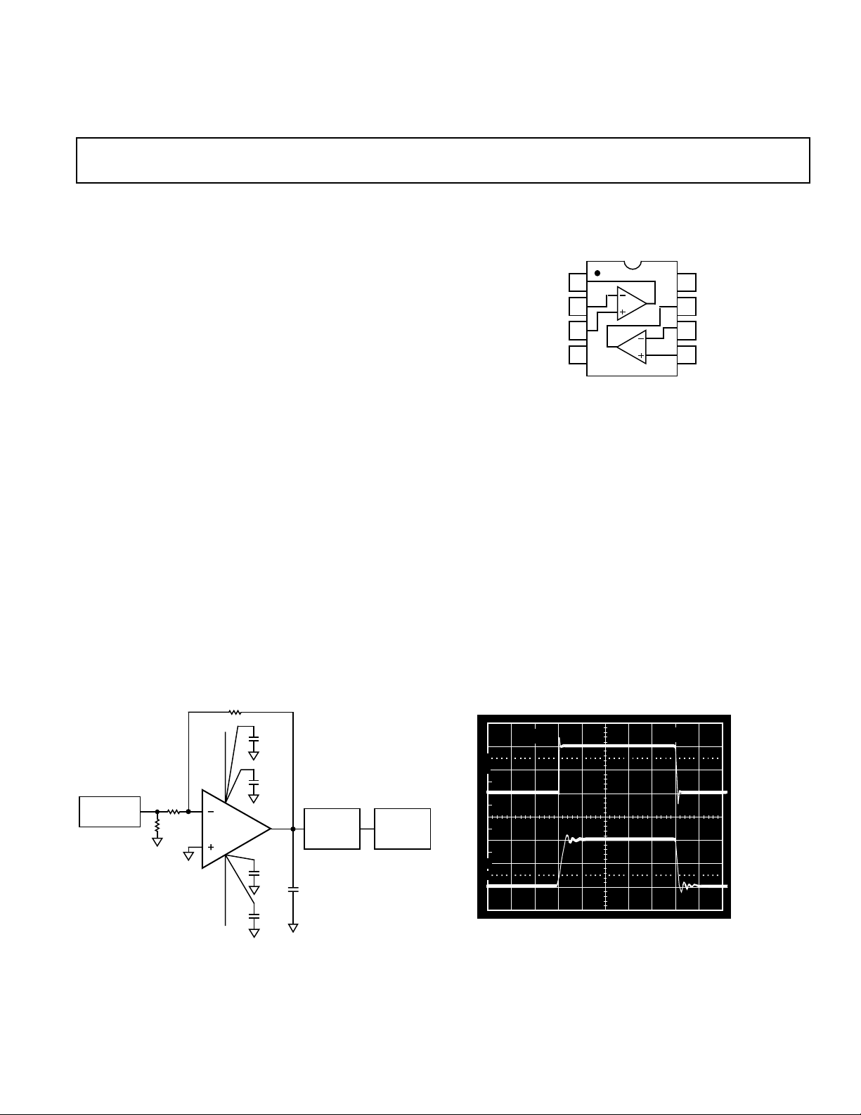
CONNECTION DIAGRAM
8-Lead Plastic Mini-DIP and SO Package
1
OUT1
2
–IN1
+IN1
3
V–
4
AD826
The AD826 features high output current drive capability of
50 mA min per amp, and is able to drive unlimited capacitive
loads. With a low power supply current of 15 mA max for both
amplifiers, the AD826 is a true general purpose operational
amplifier.
The AD826 is ideal for power sensitive applications such as video
cameras and portable instrumentation. The AD826 can operate
from a single +5 V supply, while still achieving 25 MHz of bandwidth. Furthermore the AD826 is fully specified from a single
+5 V to ±15 V power supplies.
The AD826 excels as an ADC/DAC buffer or active filter in
data acquisition systems and achieves a settling time of 70 ns
to 0.01%, with a low input offset voltage of 2 mV max. The
AD826 is available in small 8-lead plastic mini-DIP and SO
packages.
8
V+
7
OUT2
–IN2
6
+IN2
5
1k
V
S
3.3F
0.01F
V
IN
1k
50
2
3
1/2
AD826
–V
S
1
V
OUT
0.01F
3.3F
TEKTRONIX
P6201 FET
PROBE
C
L
TEKTRONIX
7A24 FET
PREAMP
Driving a Large Capacitive Load
HP PULSE
GENERATOR
REV. B
Information furnished by Analog Devices is believed to be accurate and
reliable. However, no responsibility is assumed by Analog Devices for its
use, nor for any infringements of patents or other rights of third parties
which may result from its use. No license is granted by implication or
otherwise under any patent or patent rights of Analog Devices.
One Technology Way, P.O. Box 9106, Norwood, MA 02062-9106, U.S.A.
Tel: 781/329-4700 World Wide Web Site: http://www.analog.com
Fax: 781/326-8703 © Analog Devices, Inc., 2000
Page 2

AD826–SPECIFICATIONS
(@ TA = +25C, unless otherwise noted)
Parameter Conditions V
S
Min Typ Max Unit
DYNAMIC PERFORMANCE
Unity Gain Bandwidth ±5 V 30 35 MHz
±15 V 45 50 MHz
0, +5 V 25 29 MHz
Bandwidth for 0.1 dB Flatness Gain = +1 ±5 V 10 20 MHz
±15 V 25 55 MHz
Full Power Bandwidth
1
Slew Rate R
V
= 5 V p-p
OUT
= 500 Ω±5 V 15.9 MHz
R
LOAD
V
= 20 V p-p
OUT
R
= 1 kΩ±15 V 5.6 MHz
LOAD
= 1 kΩ±5 V 200 250 V/µs
LOAD
0, +5 V 10 20 MHz
Gain = –1 ±15 V 300 350 V/µs
0, +5 V 150 200 V/µs
Settling Time to 0.1% –2.5 V to +2.5 V ±5 V 45 ns
0 V–10 V Step, A
= –1 ±15 V 45 ns
V
to 0.01% –2.5 V to +2.5 V ±5 V 70 ns
0 V–10 V Step, AV = –1 ±15 V 70 ns
NOISE/HARMONIC PERFORMANCE
Total Harmonic Distortion FC = 1 MHz ±15 V –78 dB
Input Voltage Noise f = 10 kHz ±5 V, ± 15 V 15 nV/√Hz
Input Current Noise f = 10 kHz ±5 V, ± 15 V 1.5 pA/√Hz
Differential Gain Error NTSC ±15 V 0.07 0.1 %
(R1 = 150 Ω) Gain = +2 ±5 V 0.12 0.15 %
0, +5 V 0.15 %
Differential Phase Error NTSC ±15 V 0.11 0.15 Degrees
(R1 = 150 Ω) Gain = +2 ±5 V 0.12 0.15 Degrees
0, +5 V 0.15 Degrees
DC PERFORMANCE
Input Offset Voltage ±5 V to ±15 V 0.5 2 mV
T
MIN
to T
MAX
3mV
Offset Drift 10 µV/°C
Input Bias Current ±5 V, ± 15 V 3.3 6.6 µA
T
T
MIN
MAX
10 µA
4.4 µA
Input Offset Current ±5 V, ± 15 V 25 300 nA
T
MIN
to T
MAX
500 nA
Offset Current Drift 0.3 nA/°C
Open-Loop Gain V
= ±2.5 V ±5 V
OUT
R
= 500 Ω 2 4 V/mV
LOAD
T
to T
R
V
R
T
V
R
MIN
LOAD
OUT
LOAD
MIN
OUT
LOAD
MAX
= 150 Ω 1.5 3 V/mV
= ±10 V ±15 V
= 1 kΩ 3.5 6 V/mV
to T
MAX
= ±7.5 V ±15 V
= 150 Ω (50 mA Output) 2 4 V/mV
1.5 V/mV
2 5 V/mV
INPUT CHARACTERISTICS
Input Resistance 300 kΩ
Input Capacitance 1.5 pF
Input Common-Mode Voltage Range ± 5 V +3.8 +4.3 V
–2.7 –3.4 V
±15 V +13 +14.3 V
–12 –13.4 V
0, +5 V +3.8 +4.3 V
+1.2 +0.9 V
Common-Mode Rejection Ratio V
= ±2.5 V, T
CM
V
= ±12 V ±15 V 86 120 dB
CM
T
to T
MIN
MIN–TMAX
MAX
±5 V 80 100 dB
±15 V 80 100 dB
–2–
REV. B
Page 3
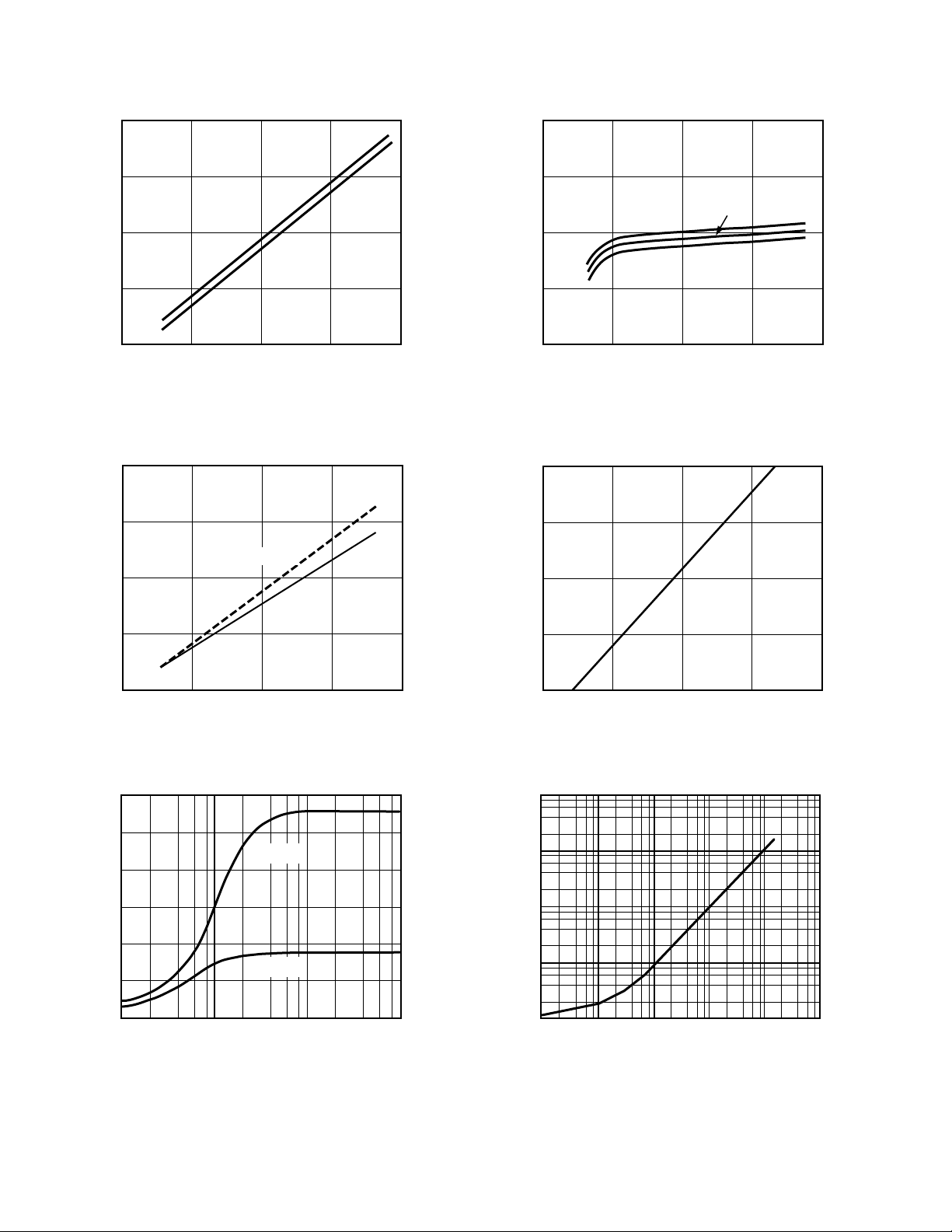
AD826
2.0
0
–50 90
1.5
0.5
–30
1.0
50 703010–10
80–40 40 60200–20
AMBIENT TEMPERATURE – C
MAXIMUM POWER DISSIPATION – Watts
8-LEAD MINI-DIP PACKAGE
8-LEAD SOIC PACKAGE
TJ = +150C
Parameter Conditions V
OUTPUT CHARACTERISTICS
Output Voltage Swing R
Output Current ±15 V 50 mA
Short-Circuit Current ± 15 V 90 mA
Output Resistance Open Loop 8 Ω
MATCHING CHARACTERISTICS
Dynamic
Crosstalk f = 5 MHz ±15 V –80 dB
Gain Flatness Match G = +1, f = 40 MHz ±15 V 0.2 dB
Slew Rate Match G = –1 ±15 V 10 V/µs
DC
Input Offset Voltage Match T
Input Bias Current Match T
Open-Loop Gain Match V
Common-Mode Rejection Ratio Match V
Power Supply Rejection Ratio Match ± 5 V to ±15 V, T
POWER SUPPLY
Operating Range Dual Supply ±2.5 ± 18 V
Quiescent Current/Amplifier ±5 V 6.6 7.5 mA
Power Supply Rejection Ratio VS = ±5 V to ±15 V, T
NOTES
1
Full power bandwidth = slew rate/2 π V
Specifications subject to change without notice.
ABSOLUTE MAXIMUM RATINGS
Supply Voltage . . . . . . . . . . . . . . . . . . . . . . . . . . . . . . . ±18 V
Internal Power Dissipation
2
Plastic (N) . . . . . . . . . . . . . . . . . . . . . See Derating Curves
Small Outline (R) . . . . . . . . . . . . . . . . See Derating Curves
Input Voltage (Common Mode) . . . . . . . . . . . . . . . . . . . ±V
Differential Input Voltage . . . . . . . . . . . . . . . . . . . . . . . ±6 V
Output Short Circuit Duration . . . . . . . See Derating Curves
Storage Temperature Range (N, R) . . . . . . . –65°C to +125°C
Operating Temperature Range . . . . . . . . . . –40°C to +85°C
Lead Temperature Range (Soldering 10 seconds) . . . +300°C
NOTES
1
Stresses above those listed under Absolute Maximum Ratings may cause perma-
nent damage to the device. This is a stress rating only; functional operation of the
device at these or any other conditions above those indicated in the operational
section of this specification is not implied. Exposure to absolute maximum rating
conditions for extended periods may affect device reliability .
2
Specification is for device in free air: 8-lead plastic package, θJA = 100°C/watt;
8-lead SOIC package, θJA = 155°C/watt.
ORDERING GUIDE
Model Range Description Option
Temperature Package Package
AD826AN – 40°C to +85°C 8-Lead Plastic DIP N-8
AD826AR –40°C to +85°C 8-Lead Plastic SOIC SO-8
AD826AR-REEL7 –40°C to +85°C 7” Tape & Reel SOIC SO-8
AD826AR-REEL –40°C to +85°C 13” Tape & Reel SOIC SO-8
REV. B
PEAK
S
= 500 Ω±5 V 3.3 3.8 ±V
LOAD
= 150 Ω±5 V 3.2 3.6 ±V
R
LOAD
= 1 kΩ±15 V 13.3 13.7 ±V
R
LOAD
= 500 Ω±15 V 12.8 13.4 ±V
R
LOAD
= 500 Ω 0, +5 V +1.5,
R
LOAD
Min Typ Max Unit
+3.5 V
±5 V 50 mA
0, +5 V 30 mA
MIN–TMAX
MIN–TMAX
= ±10 V, R
O
T
MIN–TMAX
= ±12 V, T
CM
= 1 kΩ,
LOAD
MIN–TMAX
MIN–TMAX
±5 V to ±15 V 0.5 2 mV
±5 V to ±15 V 0.06 0.8 µA
±15 V 0.15 0.01 mV/V
±15 V 80 100 dB
80 100 dB
Single Supply +5 +36 V
T
MIN
to T
MAX
±5 V 7.5 mA
±15 V 7.5 mA
T
to T
MIN
.
MAX
to T
MIN
ESD SUSCEPTIBILITY
±15 V 6.8 7.5 mA
MAX
75 86 dB
ESD (electrostatic discharge) sensitive device. Electrostatic charges
1
as high as 4000 volts, which readily accumulate on the human
body and on test equipment, can discharge without detection.
Although the AD826 features proprietary ESD protection circuitry, permanent damage may still occur on these devices
if they are subjected to high energy electrostatic discharges.
Therefore, proper ESD precautions are recommended to avoid
any performance degradation or loss of functionality.
S
Maximum Power Dissipation vs. Temperature for Different
Package Types
–3–
Page 4
AD826
– Typical Characteristics
20
15
+V
CM
10
–V
CM
5
INPUT COMMON-MODE RANGE – Volts
0
020
5
SUPPLY VOLTAGE – Volts
10
15
Figure 1. Common-Mode Voltage Range vs. Supply
7.7
7.2
6.7
6.2
QUIESCENT SUPPLY CURRENT PER AMP – mA
5.7
020
Figure 4. Quiescent Supply Current per Amp vs. Supply
Voltage for Various Temperatures
20
15
RL = 500V
10
RL = 150V
5
OUTPUT VOLTAGE SWING – Volts
400
350
300
SLEW RATE – V/s
250
–40C
5
SUPPLY VOLTAGE – Volts
10
+85
C
+25C
15
0
020
5
SUPPLY VOLTAGE – Volts
10
15
Figure 2. Output Voltage Swing vs. Supply
30
25
VS = 15V
20
15
10
5
OUTPUT VOLTAGE SWING – Volts p-p
0
10
100
LOAD RESISTANCE –
VS = 5V
1k
10k
Figure 3. Output Voltage Swing vs. Load Resistance
200
Figure 5. Slew Rate vs. Supply Voltage
100
10
1
0.1
CLOSED-LOOP OUTPUT IMPEDANCE –
0.01
1k 10k 100M10M1M100k
Figure 6. Closed-Loop Output Impedance vs. Frequency
SUPPLY VOLTAGE – Volts
20501510
FREQUENCY – Hz
–4–
REV. B
Page 5
AD826
7
6
5
4
3
INPUT BIAS CURRENT – A
2
1
–40
–60
TEMPERATURE – C
120806040 100200–20
Figure 7. Input Bias Current vs. Temperature
130
110
SOURCE CURRENT
90
SINK CURRENT
70
50
SHORT CIRCUIT CURRENT – mA
140
OPEN-LOOP GAIN – dB
100
–20
80
GAIN 15V SUPPLIES
60
40
20
0
RL = 1k
1k
GAIN 5V SUPPLIES
10k
FREQUENCY – Hz
PHASE 5V OR
15V SUPPLIES
100M10M1M100k
1G
Figure 10. Open-Loop Gain and Phase Margin
vs. Frequency
7
6
5
4
3
OPEN-LOOP GAIN – V/mV
2
15V
5V
+100
+80
+60
+40
+20
0
PHASE MARGIN – Degrees
30
–40
–60
TEMPERATURE – C
140
120100806040200–20
Figure 8. Short Circuit Current vs. Temperature
100
80
60
PHASE MARGIN – Degrees
40
20
–60 140
–40
GAIN BANDWIDTH
TEMPERATURE – C
PHASE MARGIN
100 120806040200–20
80
60
40
20
Figure 9. Unity Gain Bandwidth and Phase Margin
vs. Temperature
UNITY GAIN BANDWIDTH – MHz
1
100 1k 10k
LOAD RESISTANCE –
Figure 11. Open-Loop Gain vs. Load Resistance
100
90
PSR – dB
80
70
60
50
40
30
20
10
NEGATIVE
SUPPLY
1k100
POSITIVE
SUPPLY
FREQUENCY – Hz
100M
10M1M100k10k
Figure 12. Power Supply Rejection vs. Frequency
REV. B
–5–
Page 6

AD826
140
120
100
CMR – dB
80
60
1k 10M
10k
100k
FREQUENCY – Hz
1M
Figure 13. Common-Mode Rejection vs. Frequency
30
RL = 1k
20
–40
VIN = 1V p-p
GAIN = +2
–50
–60
–70
HARMONIC DISTORTION – dB
–100
–80
–90
100
1k
2ND HARMONIC
3RD HARMONIC
1M100k10k
FREQUENCY – Hz
Figure 16. Harmonic Distortion vs. Frequency
50
40
30
10M
10
OUTPUT VOLTAGE – Volts p-p
0
100k 1M 100M10M
RL = 150
FREQUENCY – Hz
Figure 14. Large Signal Frequency Response
10
8
6
4
1%
2
0
–2
1%
–4
–6
OUTPUT SWING FROM 0 TO V
–8
–10
0
0.1%
0.01%
0.01%
0.1%
20
SETTLING TIME – ns
160
140120100806040
Figure 15. Output Swing and Error vs. Settling Time
10
INPUT VOLTAGE NOISE – nV/ Hz
0
10203
FREQUENCY – Hz
1M100k10k1k100
10M
Figure 17. Input Voltage Noise Spectral Density
380
360
340
SLEW RATE – V/s
320
300
–60 140
–40
TEMPERATURE – C
100 120806040200–20
Figure 18. Slew Rate vs. Temperature
–6–
REV. B
Page 7

AD826
FREQUENCY – Hz
GAIN – dB
1.0
0
–1.0
100k 1M 100M10M
–0.2
–0.4
–0.6
–0.8
0.2
0.4
0.6
0.8
VS = 15V
VS = 5V
VS = +5V
1/2
AD826
3
2
1
USE GROUND PLANE
PINOUT SHOWN IS FOR MINIDIP PACKAGE
V
IN
V
S
8
RL = 150 FOR VS = 5V, 1k FOR VS = 15V
R
L
1F
0.1F
1/2
AD826
5
6
7
4
R
L
–V
S
1F
0.1F
V
OUT
5
4
3
2
1
0
GAIN – dB
–1
–2
–3
–4
–5
100k 1M 100M10M
781
V
V
IN
OUT
150
FREQUENCY – Hz
VS = 5V
V
S
15V
5V
5V
VS = 15V
VS = 5V
0.1dB
FLATNESS
55MHz
20MHz
20MHz
Figure 19. Closed-Loop Gain vs. Frequency
DIFF GAIN
0.13
0.13
0.10
0.07
5
4
V
3
2
1
0
GAIN – dB
–1
–2
–3
–4
–5
100k 1M 100M10M
1k
1k
IN
C
C
V
OUT
VS = 5V
VS = 5V
FREQUENCY – HZ
V
SCC
15V 3pF 16MHz
5V 4pF 14MHz
5V 6pF 12MHz
0.1dB
FLATNESS
VS = 15V
Figure 22. Closed-Loop Gain vs. Frequency, Gain = –1
0.12
0.11
0.10
DIFFERENTIAL PHASE – Degrees
5
Figure 20. Differential Gain and Phase vs. Supply Voltage
–30
–40
–50
–60
–70
–80
CROSSTALK – dB
–90
–100
–110
REV. B
Figure 21. Crosstalk vs. Frequency
DIFF PHASE
SUPPLY VOLTAGE – Volts
100k 100M10M1M10k
FREQUENCY – Hz
10
R
5V
= 150
L
DIFFERENTIAL GAIN – Percent
15
Figure 23. Gain Flatness Matching vs. Supply, G = +1
15V
= 1k
R
L
Figure 24. Crosstalk Test Circuit
–7–
Page 8

AD826
1k
V
S
3.3F
0.01F
V
TEKTRONIX
PULSE (LS)
OR
FUNCTION (SS)
GENERATOR
R
V
IN
100
50
1/2
IN
AD826
–V
S
OUT
0.01F
3.3F
P6201 FET
R
L
Figure 25. Noninverting Amplifier Configuration
PROBE
TEKTRONIX
7A24
PREAMP
5V
100
90
10
0%
50ns
5V
Figure 26. Noninverting Large Signal Pulse Response,
= 1 k
R
Ω
L
5V
100
90
50ns
200mV
100
90
10
0%
50ns
200mV
Figure 28. Noninverting Small Signal Pulse Response,
= 1 k
R
Ω
L
5V
200mV
100
90
50ns
10
0%
5V
Figure 27. Noninverting Large Signal Pulse Response,
R
= 150
L
Ω
10
0%
200mV
Figure 29. Noninverting Small Signal Pulse Response,
= 150
R
L
Ω
–8–
REV. B
Page 9

AD826
1k
V
S
3.3F
0.01F
TEKTRONIX
R
L
P6201 FET
PROBE
V
OUT
0.01F
3.3F
S
TEKTRONIX
7A24
PREAMP
PULSE (LS)
OR FUNCTION (SS)
GENERATOR
R
IN
1k
V
IN
50
1/2
AD826
–V
Figure 30. Inverting Amplifier Configuration
5V
100
90
10
0%
50ns
5V
200mV
100
90
10
0%
50ns
200mV
Figure 31. Inverting Large Signal Pulse Response,
= 1 k
R
Ω
L
5V
100
90
10
0%
50ns
5V
Figure 32. Inverting Large Signal Pulse Response,
= 150
R
L
Ω
Figure 33. Inverting Small Signal Pulse Response,
= 1 k
R
Ω
L
200mV
100
90
10
0%
50ns
200mV
Figure 34. Inverting Small Signal Pulse Response,
= 150
R
L
Ω
REV. B
–9–
Page 10

AD826
THEORY OF OPERATION
The AD826 is a low cost, wide band, high performance dual
operational amplifier which can drive heavy capacitive and
resistive loads. It also achieves a constant slew rate, bandwidth
and settling time over its entire specified temperature range.
The AD826 (Figure 35) consists of a degenerated NPN differential pair driving matched PNPs in a folded-cascode gain stage.
The output buffer stage employs emitter followers in a class AB
amplifier which delivers the necessary current to the load while
maintaining low levels of distortion.
+V
S
C
F
–IN
+IN
NULL 1 NULL 8
OUTPUT
–V
S
Figure 35. Simplified Schematic
The capacitor, CF, in the output stage mitigates the effect of
capacitive loads. With low capacitive loads, the gain from the
compensation node to the output is very close to unity. In this
case, C
is bootstrapped and does not contribute to the overall
F
compensation capacitance of the device. As the capacitive load
is increased, a pole is formed with the output impedance of the
output stage. This reduces the gain, and therefore, C
incompletely bootstrapped. Effectively, some fraction of C
is
F
F
contributes to the overall compensation capacitance, reducing
the unity gain bandwidth. As the load capacitance is further
increased, the bandwidth continues to fall, maintaining the
stability of the amplifier.
INPUT CONSIDERATIONS
An input protection resistor (RIN in Figure 25) is required in
circuits where the input to the AD826 will be subjected to
transient or continuous overload voltages exceeding the ± 6 V
maximum differential limit. This resistor provides protection for
the input transistors by limiting their maximum base current.
For high performance circuits, it is recommended that a “balancing” resistor be used to reduce the offset errors caused by
bias current flowing through the input and feedback resistors.
The balancing resistor equals the parallel combination of R
IN
and RF and thus provides a matched impedance at each input
terminal. The offset voltage error will then be reduced by more
than an order of magnitude.
APPLYING THE AD826
The AD826 is a breakthrough dual amp that delivers precision
and speed at low cost with low power consumption. The AD826
offers excellent static and dynamic matching characteristics,
combined with the ability to drive heavy resistive and capacitive
loads.
As with all high frequency circuits, care should be taken to maintain overall device performance as well as their matching. The
following items are presented as general design considerations.
Circuit Board Layout
Input and output runs should be laid out so as to physically
isolate them from remaining runs. In addition, the feedback
resistor of each amplifier should be placed away from the
feedback resistor of the other amplifier, since this greatly
reduces inter-amp coupling.
Choosing Feedback and Gain Resistors
In order to prevent the stray capacitance present at each amplifier’s
summing junction from limiting its performance, the feedback
resistors should be ≤ 1 kΩ. Since the summing junction capacitance may cause peaking, a small capacitor (1 pF–5 pF) may
be paralleled with R
to neutralize this effect. Finally, sockets
F
should be avoided, because of their tendency to increase interlead
capacitance.
Power Supply Bypassing
Proper power supply decoupling is critical to preserve the
integrity of high frequency signals. In carefully laid out designs,
decoupling capacitors should be placed in close proximity to the
supply pins, while their lead lengths should be kept to a minimum. These measures greatly reduce undesired inductive effects
on the amplifier’s response.
Though two 0.1 µF capacitors will typically be effective in
decoupling the supplies, several capacitors of different values
can be paralleled to cover a wider frequency range.
–10–
REV. B
Page 11

AD826
SINGLE SUPPLY OPERATION
An exciting feature of the AD826 is its ability to perform well in a
single supply configuration (see Figure 37). The AD826 is ideally
suited for applications that require low power dissipation and high
output current and those which need to drive large capacitive
loads, such as high speed buffering and instrumentation.
Referring to Figure 36, careful consideration should be given to
the proper selection of component values. The choices for this
particular circuit are: (R1 + R3)储R2 combine with C1 to form a
low frequency corner of approximately 30 Hz.
V
S
R3
0.1F
V
IN
1k
C2
R1
9k
C1
1F
R2
10k
1/2
AD826
3.3F
0.01F
150
0.1F
C
OUT
V
OUT
R
C3
C
L
L
200pF
Figure 36. Single Supply Amplifier Configuration
R3 and C2 reduce the effect of the power supply changes on the
1
output by low-pass filtering with a corner at
The values for R
and CL were chosen to demonstrate the
L
2πR
3C2
.
AD826’s exceptional output drive capability. In this configuration, the output is centered around 2.5 V. In order to eliminate
the static dc current associated with this level, C3 was inserted
in series with R
.
L
500mV
100
90
10
0%
500mV
100ns
Figure 37. Single Supply Pulse Response, G = +1,
= 150Ω, CL = 200 pF
R
L
PARALLEL AMPS PROVIDE 100 mA TO LOAD
By taking advantage of the superior matching characteristics of
the AD826, enhanced performance can easily be achieved by
employing the circuit in Figure 38. Here, two identical cells are
paralleled to obtain even higher load driving capability than that
of a single amplifier (100 mA min guaranteed). R1 and R2 are
included to limit current flow between amplifier outputs that
would arise in the presence of any residual mismatch.
1k
V
1F
S
1/2
AD826
1/2
AD826
–V
S
1k
0.1F
0.1F
1F
5
R1
R2
5
V
OUT
1k
V
1k
IN
Figure 38. Parallel Amp Configuration
R
L
REV. B
–11–
Page 12

AD826
SINGLE-ENDED TO DIFFERENTIAL LINE DRIVER
Outstanding CMRR (> 80 dB @ 5 MHz), high bandwidth, wide
supply voltage range, and the ability to drive heavy loads, make
the AD826 an ideal choice for many line driving applications.
In this application, the AD830 high speed video difference
amp serves as the differential line receiver on the end of a back
terminated, 50 ft., twisted-pair transmission line (see Figure 40).
The overall system is configured in a gain of +1 and has a –3 dB
bandwidth of 14 MHz. Figure 39 is the pulse response with a
2 V p-p, 1 MHz signal input.
2V
100
90
10
0%
200ns
2V
Figure 39. Pulse Response
15V
0.01F
50 FEET TWISTED PAIR
I
N
BNC
1.05k
5pF
1.05k
5pF
1/2
AD826
1.05k
1.05k
1/2
AD826
–15V
0.1F
0.01F
0.1F
2.2F
36
36
2.2F
Z = 72
Figure 40. Differential Line Driver
LOW DISTORTION LINE DRIVER
The AD826 can quickly be turned into a powerful, low distortion line driver (see Figure 41). In this arrangement the AD826
can comfortably drive a 75 Ω back-terminated cable, with a
5 MHz, 2 V p-p input; all of this while achieving the harmonic
distortion performance outlined in the following table.
Configuration 2nd Harmonic
1. No Load –78.5 dBm
2. 150 Ω RL Only –63.8 dBm
3. 150 Ω RL 7.5 Ω R
C
–70.4 dBm
In this application one half of the AD826 operates at a gain of
2.1 and supplies the current to the load, while the other provides the overall system gain of 2. This is important for two
reasons: the first is to keep the bandwidth of both amplifiers the
same, and the second is to preserve the AD826’s ability to operate from low supply voltages. R
varies with the load and must
C
be chosen to satisfy the following equation:
R
= MR
C
L
where M is defined by [(M+ 1) GS = GD] and GD = Driver’s Gain,
G
= System Gain.
S
–12–
15V 0.01F
0.1F
36
AD830
36
0.01F
–15V
0.1F
1.1k
V
1F
1k
1k
75
S
1/2
AD826
1k
1/2
AD826
0.1F
1F
0.1F
Figure 41. Low Distortion Amplifier
R
C
7.5
75
V
OUT
R
L
75
REV. B
Page 13

AD826
HIGH PERFORMANCE ADC BUFFER
Figure 42 is a schematic of a 12-bit high speed analog-to-digital
converter. The AD826 dual op amp takes a single ended input
and drives the AD872 A/D converter differentially, thus reducing 2nd harmonic distortion. Figure 43 is a FFT of a 1 MHz
input, sampled at 10 MHz with a THD of –78 dB. The AD826
can be used to amplify low level signals so that the entire range
of the converter is used. The ability of the AD826 to perform on
a ±5 volt supply or even with a single 5 volts combined with its
rapid settling time and ability to deliver high current to complicated loads make it a very good flash A/D converter buffer as
well as a very useful general purpose building block.
1k
V
S
1k
1/2
AD826
V
500mV
p-p MAX
50
COAX
CABLE
IN
52.5
1/2
AD826
–V
1k
S
5V
COMMON
–5V
100F
25V
100F
25V
V
–V
1k
S
S
Figure 42. A Differential Input Buffer for High
Bandwidth ADCs
0.1F
0.1F
V
INA
AD872
12-BIT
10MSPS
ADC
V
INB
REV. B
Figure 43. FFT, Buffered A/D Converter
–13–
Page 14

AD826
OUTLINE DIMENSIONS
Dimensions shown in inches and (mm).
8-Lead Plastic Mini-DIP (N) Package
0.165±0.01
(4.19±0.25)
0.1574 (4.00)
0.1497 (3.80)
PIN 1
0.0098 (0.25)
0.0040 (0.10)
SEATING
8
PIN 1
1
0.125
(3.18)
MIN
0.018±0.003
(0.46±0.08)
0.1968 (5.00)
0.1890 (4.80)
85
0.0500 (1.27)
PLANE
5
0.25
(6.35)
0.31
0.39 (9.91) MAX
0.10
(2.54)
BSC
4
0.033
(0.84)
NOM
0.035±0.01
(0.89±0.25)
0.18±0.03
(4.57±0.76)
SEATING
PLANE
(7.87)
8-Lead SO (R) Package
0.2440 (6.20)
0.2284 (5.80)
41
BSC
0.0192 (0.49)
0.0138 (0.35)
0.0688 (1.75)
0.0532 (1.35)
0.0098 (0.25)
0.0075 (0.19)
0.30 (7.62)
REF
0.011±0.003
(0.28±0.08)
15
°
0
°
0.0196 (0.50)
0.0099 (0.25)
8
0.0500 (1.27)
0
0.0160 (0.41)
C1807a–0–6/00 (rev. B) 00877
45
All brand or product names mentioned are trademarks or registered trademarks of their respective holders.
–14–
REV. B
PRINTED IN U.S.A.
 Loading...