

Page 1
Low Cost, General Purpose
a
FEATURES
High Speed
41 MHz, –3 dB Bandwidth
125 V/s Slew Rate
80 ns Settling Time
Input Bias Current of 20 pA and Noise Current of
10 fA/√Hz
Input Voltage Noise of 12 nV/√Hz
Fully Specified Power Supplies: ⴞ5 V to ⴞ15 V
Low Distortion: –76 dB at 1 MHz
High Output Drive Capability
Drives Unlimited Capacitance Load
50 mA Min Output Current
No Phase Reversal When Input Is at Rail
Available in 8-Lead SOIC
APPLICATIONS
CCD
Low Distortion Filters
Mixed Gain Stages
Audio Amplifier
Photo Detector Interface
ADC Input Buffer
DAC Output Buffer
High Speed JFET Amplifier
AD825
CONNECTION DIAGRAM
8-Lead Plastic SOIC (R) Package
NC
–IN
+IN
–V
1
2
3
S
4
AD825
TOP VIEW
(Not to Scale)
NC = NO CONNECT
8
7
6
5
NC
+V
S
OUTPUT
NC
PRODUCT DESCRIPTION
The AD825 is a superbly optimized operational amplifier for
high speed, low cost and dc parameters, making it ideally suited
for a broad range of signal conditioning and data acquisition
applications. The ac performance, gain, bandwidth, slew rate
and drive capability are all very stable over temperature. The
AD825 also maintains stable gain under varying load conditions.
The unique input stage has ultralow input bias current and
ultralow input current noise. Signals that go to either rail on this
high performance input do not cause phase reversals at the output.
These features make the AD825 a good choice as a buffer for
MUX outputs, creating minimal offset and gain errors.
The AD825 is fully specified for operation with dual ±5 V and
±15 V supplies. This power supply flexibility, and the low sup-
ply current of 6.5 mA with excellent ac characteristics under all
supply conditions, makes the AD825 well suited for many
demanding applications.
REV. C
Information furnished by Analog Devices is believed to be accurate and
reliable. However, no responsibility is assumed by Analog Devices for its
use, nor for any infringements of patents or other rights of third parties
which may result from its use. No license is granted by implication or
otherwise under any patent or patent rights of Analog Devices.
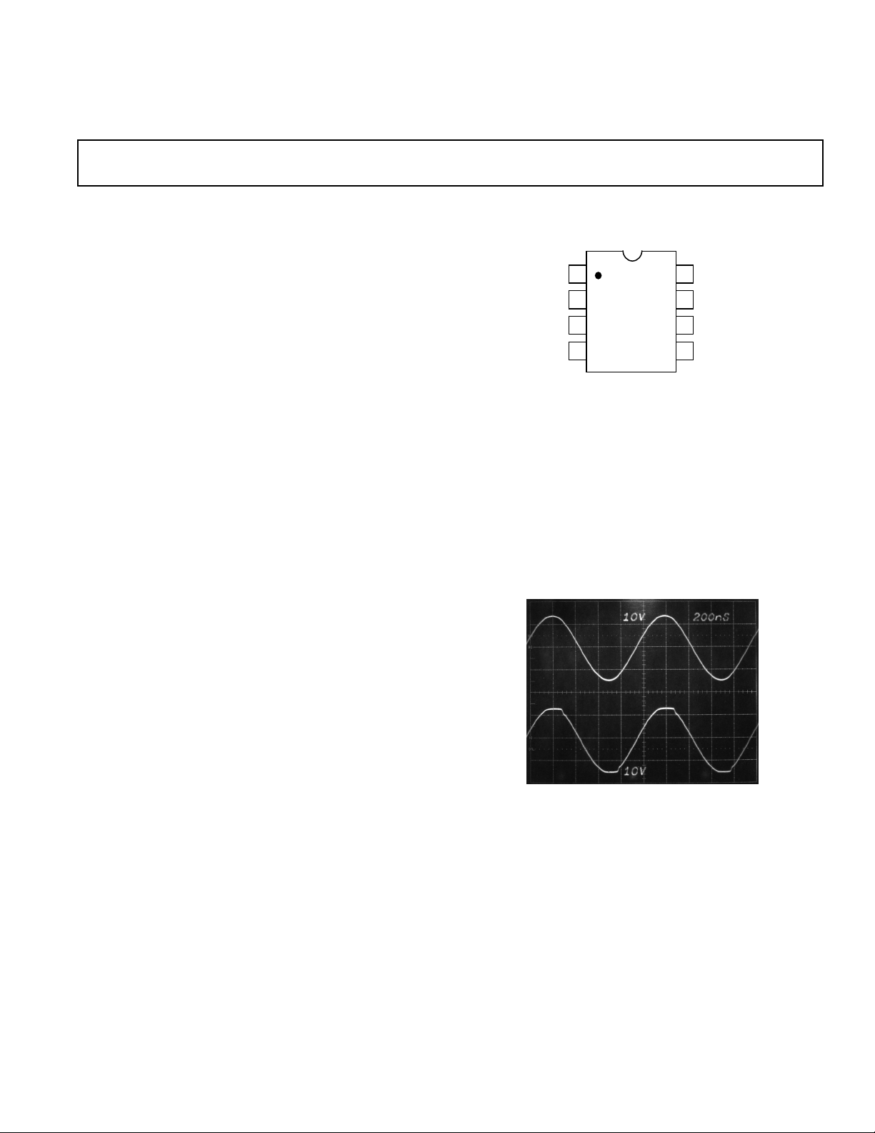
Figure 1. Performance with Rail-to-Rail Input Signals
One Technology Way, P.O. Box 9106, Norwood, MA 02062-9106, U.S.A.
Tel: 781/329-4700 World Wide Web Site: http://www.analog.com
Fax: 781/326-8703 © Analog Devices, Inc., 1999
Page 2

AD825–SPECIFICATIONS
(@ TA = +25ⴗC, VS = ⴞ15 V unless otherwise noted)
␣␣␣␣␣␣␣␣ AD825A
Parameter Conditions V
S
Min Typ Max Units
DYNAMIC PERFORMANCE
Unity Gain Bandwidth ±15 V 23 26 MHz
Bandwidth for 0.1 dB Flatness Gain = +1 ±15 V 18 21 MHz
–3 dB Bandwidth Gain = +1 ±15 V 44 46 MHz
Slew Rate R
Settling Time to 0.1% 0 V–10 V Step, A
Settling Time to 0.01% 0 V–10 V Step, A
Total Harmonic Distortion F
= 1 kΩ, G = 1 ±15 V 125 140 V/µs
LOAD
= 1 MHz, G = –1 ±15 V –77 dB
C
= –1 ±15 V 150 180 ns
V
= –1 ±15 V 180 220 ns
V
Differential Gain Error NTSC ±15 V 1.3 %
= 150 Ω) Gain = +2
(R
LOAD
Differential Phase Error NTSC ±15 V 2.1 Degrees
(R
= 150 Ω) Gain = +2
LOAD
INPUT OFFSET VOLTAGE ±15 V 1 2 mV
T
MIN
to T
MAX
5mV
Offset Drift 10 µV/°C
INPUT BIAS CURRENT ±15 V 15 40 pA
T
T
MIN
MAX
5pA
700 pA
INPUT OFFSET CURRENT ±15 V 20 30 pA
OPEN LOOP GAIN V
T
MIN
T
MAX
= ±10 V ±15 V
OUT
R
= 1 kΩ 70 76 dB
LOAD
V
= ±7.5 V ±15 V
OUT
= 1 kΩ 70 76 dB
R
LOAD
V
= ±7.5 V ±15 V
OUT
R
= 150 Ω 72 74 dB
LOAD
5pA
440 pA
(50 mA Output)
COMMON-MODE REJECTION V
= ±10 V ±15 V 71 80 dB
CM
INPUT VOLTAGE NOISE f = 10 kHz ±15 V 12 nV/√Hz
INPUT CURRENT NOISE f = 10 kHz ±15 V 10 fA/√Hz
INPUT COMMON-MODE
VOLTAGE RANGE ±15 V ±13.5 V
OUTPUT VOLTAGE SWING R
= 1 kΩ±15 V 13 ±13.3 V
LOAD
R
= 500 Ω±15 V 12.9 ±13.2 V
LOAD
Output Current ±15 V 50 mA
Short-Circuit Current ±15 V 100 mA
INPUT RESISTANCE 5 × 10
11
Ω
INPUT CAPACITANCE 6pF
OUTPUT RESISTANCE Open Loop 8 Ω
POWER SUPPLY
Quiescent Current ±15 V 6.5 7.2 mA
T
to T
MIN
NOTES
All limits are determined to be at least four standard deviations away from mean value.
Specifications subject to change without notice.
MAX
–2–
±15 V 7.5 mA
.
REV. C
Page 3

SPECIFICATIONS
Parameter Conditions V
DYNAMIC PERFORMANCE
Unity Gain Bandwidth ±5 V 18 21 MHz
Bandwidth for 0.1 dB Flatness Gain = +1 ±5 V 8 10 MHz
–3 dB Bandwidth Gain = +1 ±5 V 34 37 MHz
Slew Rate R
Settling Time to 0.1% –2.5 V to +2.5 V ±5 V 75 90 ns
Settling Time to 0.01% –2.5 V to +2.5 V ±5 V 90 110 ns
Total Harmonic Distortion F
Differential Gain Error NTSC ±5 V 1.2 %
= 150 Ω) Gain = +2
(R
LOAD
Differential Phase Error NTSC ±5 V 1.4 Degrees
(R
= 150 Ω) Gain = +2
LOAD
INPUT OFFSET VOLTAGE ±5 V 1 2 mV
Offset Drift 10 µV/°C
INPUT BIAS CURRENT ±5 V 10 30 pA
INPUT OFFSET CURRENT ±5 V 15 25 pA
Offset Current Drift T
OPEN LOOP GAIN V
COMMON-MODE REJECTION V
INPUT VOLTAGE NOISE f = 10 kHz ±5 V 12 nV/√Hz
INPUT CURRENT NOISE f = 10 kHz ±5 V 10 fA/√Hz
INPUT COMMON-MODE
VOLTAGE RANGE ±5 V ±3.5 V
OUTPUT VOLTAGE SWING R
Output Current ±5 V 50 mA
Short-Circuit Current ±5 V 80 mA
INPUT RESISTANCE 5 × 10
(@ TA = +25ⴗC, VS = ⴞ5 V unless otherwise noted)
S
= 1 kΩ, G = –1 ±5 V 115 130 V/µs
LOAD
= 1 MHz, G = –1 ±5 V –76 dB
C
T
to T
T
T
T
OUT
R
LOAD
R
LOAD
CM
LOAD
R
LOAD
MIN
MIN
MAX
MIN
MAX
MAX
= ±2.5 V ±5 V
= 500 Ω 64 66 dB
= 150 Ω 64 66 dB
= ±2 V ±5 V 69 80 dB
= 500 Ω 3.2 ±3.4 V
= 150 Ω±5 V 3.1 ±3.2 V
␣␣␣␣␣␣␣␣ AD825A
Min Typ Max Units
5mV
5pA
600 pA
5pA
280 pA
11
Ω
AD825
INPUT CAPACITANCE 6pF
OUTPUT RESISTANCE Open Loop 8 Ω
POWER SUPPLY
Quiescent Current ±5 V 6.2 6.8 mA
T
to T
MIN
POWER SUPPLY REJECTION V
NOTES
All limits are determined to be at least four standard deviations away from mean value.
Specifications subject to change without notice.
S
MAX
= ±5 V to ±15 V 76 88 dB
±5 V 7.5 mA
–3–REV. C
Page 4
AD825
WARNING!
ESD SENSITIVE DEVICE
ABSOLUTE MAXIMUM RATINGS
Supply␣ Voltage . . . . . . . . . . . . . . . . . . . . . . . . . . . . . . . . ±18␣ V
Internal␣ Power␣ Dissipation
2
1
Small␣ Outline␣ (R) . . . . . . . . . . . . . . . . . See Derating Curves
Input Voltage (Common Mode) . . . . . . . . . . . . . . . . . . . . ±V
Differential␣ Input␣ Voltage . . . . . . . . . . . . . . . . . . . . . . . . . ±V
S
S
Output Short Circuit Duration . . . . . . . . See Derating Curves
Storage Temperature Range R . . . . . . . . . . . –65°C to +125°C
Operating Temperature Range . . . . . . . . . . . –40°C to +85°C
Lead Temperature Range (Soldering␣ 10␣ sec) . . . . . . . .+300°C
NOTES
1
Stresses above those listed under Absolute Maximum Ratings may cause perma-
nent damage to the device. This is a stress rating only; functional operation of the
device at these or any other conditions above those indicated in the operational
section of this specification is not implied. Exposure to absolute maximum rating
conditions for extended periods may affect device reliability.
2
Specification is for device in free air: 8-lead SOIC package: θJA = 155°C/W.
PIN CONFIGURATION
1
NC
AD825
2
–IN
TOP VIEW
(Not to Scale)
+IN
3
–V
4
S
NC = NO CONNECT
2.0
1.5
1.0
0.5
MAXIMUM POWER DISSIPATION – Watts
0
–50 90–40 –30 –20 –10 0 10 20 30 50 60 70 8040
8-LEAD SOIC PACKAGE
AMBIENT TEMPERATURE – °C
8
7
6
5
NC
+V
S
OUTPUT
NC
TJ = +1508C
Figure 2. Maximum Power Dissipation vs. Temperature
ORDERING GUIDE
Temperature Package Package
Model Range Description Option
AD825AR –40°C to +85°C 8-Lead Plastic SOIC SO-8
AD825ACHIPS –40°C to +85°CDie
AD825AR-REEL –40°C to +85°C13
AD825AR-REEL7 –40°C to +85°C7
"
Tape and Reel SO-8
"
Tape and Reel SO-8
CAUTION
ESD (electrostatic discharge) sensitive device. Electrostatic charges as high as 4000 V readily
accumulate on the human body and test equipment and can discharge without detection.
Although the AD825 features proprietary ESD protection circuitry, permanent damage may
occur on devices subjected to high energy electrostatic discharges. Therefore, proper ESD
precautions are recommended to avoid performance degradation or loss of functionality.
–4–
REV. C
Page 5

Typical Characteristics–
TEMPERATURE – 8C
35
–60
140
–40
UNITY GAIN BANDWIDTH – MHz
–20 0 20 40 80 100 120
30
15
10
5
0
25
20
20
40
60
80
PHASE MARGIN – 8C
60
BANDWIDTH
PHASE MARGIN
AD825
20
15
10
5
0
–5
OUTPUT SWING – Volts
–10
–15
–20
0182
4 6 8 10 12 14 16
SUPPLY VOLTAGE – Volts
RL = 150V RL = 1kV
Figure 3. Output Voltage Swing vs. Supply
15
10
VS = 615V
5
VS = 65V
0
100
10
1
OUTPUT IMPEDANCE – V
0.1
0.01
100 10M1k
10k 100k 1M
FREQUENCY – Hz
Figure 6. Closed-Loop Output Impedance vs. Frequency
–5
OUTPUT SWING – Volts
–10
–15
Figure 4. Output Voltage Swing vs. Load Resistance
7.0
6.5
6.0
SUPPLY CURRENT – mA
5.5
5.0
Figure 5. Quiescent Supply Current vs. Supply Voltage for
Various Temperatures
0 100
0202
VS = 615V
200 300 400 500 600 700 800 900 1000
LOAD RESISTANCE – Ohms
4 6 8 10 12 14 16 18
SUPPLY VOLTAGE – ±V
–408
+258
+858
Figure 7. Unity Gain Bandwidth and Phase Margin vs.
Temperature
80
VS = 615V
70
VS = 65V
60
50
40
30
OPEN-LOOP GAIN – dB
20
10
0
1k 100M10k
100k 1M 10M
FREQUENCY – Hz
Figure 8. Open-Loop Gain and Phase Margin vs.
Frequency
–5–REV. C
180
135
90
45
0
OPEN-LOOP PHASE – Degrees
Page 6

AD825
80
75
VS = 615V
70
OPEN-LOOP GAIN – dB
65
60
100 10k1k
LOAD RESISTANCE – V
VS = 65V
Figure 9. Open-Loop Gain vs. Load Resistance
10
0
–10
–20
–30
–40
PSR – dB
–50
–60
–70
–80
–90
10k 10M100k
FREQUENCY – Hz
–PSRR
+PSRR
1M
Figure 10. Power Supply Rejection vs. Frequency
30
RL = 1kV
20
RL = 150V
10
OUTPUT VOLTAGE – Volts p-p
0
10k 100k
FREQUENCY – Hz
1M 10M
Figure 12. Large Signal Frequency Response; G = +2
200
180
160
140
120
100
80
SETTLING TIME – ns
60
40
20
0
10 –108
6 4 2 0 –2 –4 –6 –8
0.01%
0.1%
OUTPUT SWING – 0 to 6V
0.01%
0.1%
Figure 13. Output Swing and Error vs. Settling Time
130
120
110
100
90
80
CMR – dB
70
60
50
40
30
10 10M1k
100 10k 1M
VS = 615
VS = 65
100k
FREQUENCY – Hz
Figure 11. Common-Mode Rejection vs. Frequency
–6–
–50
–55
–60
–65
–70
DISTORTION – dB
–75
–80
–85
100k 10M1M
FREQUENCY – Hz
2nd
3rd
Figure 14. Harmonic Distortion vs. Frequency
REV. C
Page 7

AD825
160
140
120
100
SLEW RATE – V/ms
80
60
40
20
0
–60 140–40
65V
–20 0 20 40 80 100 120
615V
60
TEMPERATURE – 8C
Figure 15. Slew Rate vs. Temperature
2
1
0
–1
–2
–3
–4
V
GAIN – dB
IN
VS0.1dB FLATNESS
–5
65V 10MHz
–6
615V 21MHz
–7
–8
1k 100k 10M10k 1M
V
OUT
FREQUENCY – Hz
10mF
+V
S
0.01mF
V
HP
PULSE (LS)
OR FUNCTION
(SS)
GENERATOR
50V
AD825
–V
S
0.01mF
10mF
V
IN
OUT
TEKTRONIX
P6204 FET
PROBE
R
L
Figure 18. Noninverting Amplifier Connection
TEKTRONIX
7A24
PREAMP
Figure 16. Closed-Loop Gain vs. Frequency, Gain = +1
2
1
0
–1
–2
–3
GAIN – dB
–4
–5
–6
–7
–8
1k 100k 10M10k 1M
1kV 1kV
V
IN
VS0.1dB FLATNESS
65V 7.7MHz
615V 9.8MHz
V
OUT
FREQUENCY – Hz
Figure 17. Closed-Loop Gain vs. Frequency, Gain = –1
Figure 19. Noninverting Large Signal Pulse
= 1 k
Response, R
Ω
L
Figure 20.␣ Noninverting Small Signal Pulse
= 1 k
Response, R
Ω
L
–7–REV. C
Page 8

AD825
Figure 21.␣ Noninverting Large Signal Pulse
= 150
Response, R
L
Ω
Figure 22.␣ Noninverting Small Signal Pulse
= 150
Response, R
L
Ω
1kV
10mF
+V
S
Figure 24. Inverting Large Signal Pulse
= 1 k
Response, R
Ω
L
Figure 25.␣ Inverting Small Signal Pulse
Response, R
= 1 k
L
Ω
0.01mF
R
HP
PULSE
GENERATOR
IN
V
1kV
IN
50V
AD825
–V
V
OUT
0.01mF
10mF
S
Figure 23. Inverting Amplifier Connection
TEKTRONIX
P6204 FET
PROBE
C
L
1000pF
TEKTRONIX
7A24
PREAMP
–8–
REV. C
Page 9

AD825
1kV
10mF
+V
S
0.01mF
R
HP
PULSE
GENERATOR
IN
V
1kV
IN
50V
AD825
–V
V
OUT
TEKTRONIX
P6204 FET
PROBE
0.01mF
C
10mF
S
L
TEKTRONIX
7A24
PREAMP
Figure 26a.␣ Inverting Amplifier Driving a Capacitive Load
INPUT
OUTPUT
Figure 26b. Inverting Amplifier Pulse Response
While Driving a 400 pF Capacitive Loads
VPOS
NEG
POS
C
F
VOUT
DRIVING CAPACITIVE LOADS
The internal compensation of the AD825, together with its high
output current drive, permits excellent large signal performance
while driving extremely high capacitive loads.
THEORY OF OPERATION
The AD825 is a low cost, wide band, high performance FET
input operational amplifier. With its unique input stage design,
the AD825 assures no phase reversal even for inputs that exceed
the power supply voltages, and its output stage is designed to
drive heavy capacitive or resistive load with small changes relative to no load condition.
The AD825 (Figure 27) consists of common-drain commonbase FET input stage driving a cascoded, common base matched
NPN gain stage. The output buffer stage uses emitter followers
in a class AB amplifier that can deliver large current to the load
while maintaining low levels of distortion.
The capacitor, C
, in the output stage, enables the AD825 to
F
drive heavy capacitive load. For light load, the gain of the output buffer is close to unity, C
is bootstrapped and not much
F
happens. As the capacitive load is increased, the gain of the
output buffer is decreased and the bandwidth of the amplifier is
reduced through a portion of C
adding to the dominant pole.
F
As the capacitive load is further increased, the amplifier’s bandwidth continues to drop, maintaining the stability of the AD825.
Input Consideration
The AD825 with its unique input stage assures no phase reversal for signals as large or even larger than the supply voltages.
Also, layout considerations of the input transistors assure functionality even with a large differential signal.
The need for a low noise input stage calls for a larger FET transistor. One should consider the additional capacitance that is added
to assure stability. When filters are designed with the AD825,
one needs to consider the input capacitance (5 pF–6 pF) of the
AD825 as part of the passive network.
Grounding and Bypassing
The AD825 is a low input bias current FET amplifier. Its high
frequency response makes it useful in applications such as photo
diode interfaces, filters and audio circuits. When designing high
frequency circuits, some special precautions are in order. Circuits must be built with short interconnects, and resistances
should have low inductive paths to ground. Power supply leads
should be bypassed to common as close as possible to the ampli-
fier pins. Ceramic capacitors of 0.1 µF are recommended.
Figure 27. Simplified Schematic
VNEG
–9–REV. C
Page 10

AD825
Second Order Low-Pass Filter
A second order Butterworth low-pass filter can be implemented
using the AD825 as shown in Figure 28. The extremely low bias
currents of the AD825 allow the use of large resistor values, and
consequently small capacitor values, without concern for developing large offset errors. Low current noise is another factor in
permitting the use of large resistors without having to worry
about the resultant voltage noise.
With the values shown, the corner frequency will be 1 MHz.
The equations for component selection are shown below. Note
that the noninverting input (and the inverting input) has an
input capacitance of 6 pF. As a result, the calculated value of
C1 (12 pF) is reduced to 6 pF.
+5V
9.31k⍀R29.31k⍀
V
IN
C1
6pF
24pF
C2
R1
AD825
–5V
C3
0.1F
C4
0.1F
V
OUT
Figure 28. Second Order Butterworth Low-Pass Filter
C1=
C2( farads ) =
R1= R2 =user selected typically 10 kΩ to 100 kΩ
1.414
2π f
CUTOFF
R1
0.707
CUTOFF
R1
2π f
()
A plot of the filter frequency response is shown in Figure 29;
better than 40 dB of high frequency rejection is provided.
0
–10
–20
–30
–40
–50
–60
–70
HIGH FREQUENCY REJECTION – dB
–80
10k 100M100k
1M 10M
FREQUENCY – Hz
Figure 29. Frequency Response of Second Order
Butterworth Filter
–10–
REV. C
Page 11

OUTLINE DIMENSIONS
85
41
0.1 968 (5.00)
0.1 890 (4.80)
0.2440 (6.20)
0.2284 (5.80)
PIN 1
0.1574 (4.00)
0.1497 (3.80)
0.0500 (1.27)
BSC
0.0688 (1.75)
0.0532 (1.35)
SEATING
PLANE
0.0098 (0.25)
0.0040 (0.10)
0.0192 (0.49)
0.0138 (0.35)
0.0098 (0.25)
0.0075 (0.19)
0.0500 (1.27)
0.0160 (0.41)
88
08
0.0196 (0.50)
0.0099 (0.25)
3 458
Dimensions shown in inches and (mm).
8-Lead Plastic SOIC
(SO-8)
AD825
C3206c–0–12/99
PRINTED IN U.S.A.
–11–REV. C
 Loading...