

Page 1
LED Driver/Monitor
FEATURES
PWM input for LED brightness control
Open LED detection
Latch-off overcurrent protection
Constant voltage regulated output
Supply range: 9 V to 27 V
Regulated voltage range: 12.5 V to 27 V
Operating current: 300 µA
Shutdown current: 10 µA
Temperature range −40°C to +125°C
8-lead MSOP package
GENERAL DESCRIPTION
The AD8240 LED driver/monitor, in combination with an
external transistor, supplies a constant 12 V to drive LED
lamps. This allows cost-effective LED lamp monitoring and
short-circuit protection. The output is regulated at 12 V when
the supply voltage is between 12.5 V and 27 V.
A CMOS compatible, level-dependent, digital input can be used
for PWM control of the LED brightness. V
the PWM input is high and turned off when the input is low.
The AD8240 is designed to work with a PWM frequency up
to 500 Hz, and a typical PWM range from 5% to 95%.
Open LED detection is accomplished by measuring the change
in LED lamp current caused by an open LED(s) through the use
of an internal high-side current-sense amplifier that amplifies
the voltage across an external current shunt. The voltage across
the shunt resistor is amplified to a level that can be measured by
a microcontroller A/D converter or a comparator. The ability to
measure the change in LED lamp current is the key benefit of
constant-voltage LED lamp driving.
The output is current-limited by latching off the output voltage
when the current reaches a preset level. The current limit is set
by selecting the value of the external current shunt that causes
the output of the sense amplifier to slightly exceed the 5 V
reference level when the current exceeds a maximum level.
When the sense amplifier output exceeds 5 V, it trips an internal
comparator that causes the driver to latch off the output voltage.
The latch is reset during the next PWM cycle. The overcurrent
condition can also be detected by a microcontroller or external
comparator by measuring the sense amplifier output.
is turned on when
O
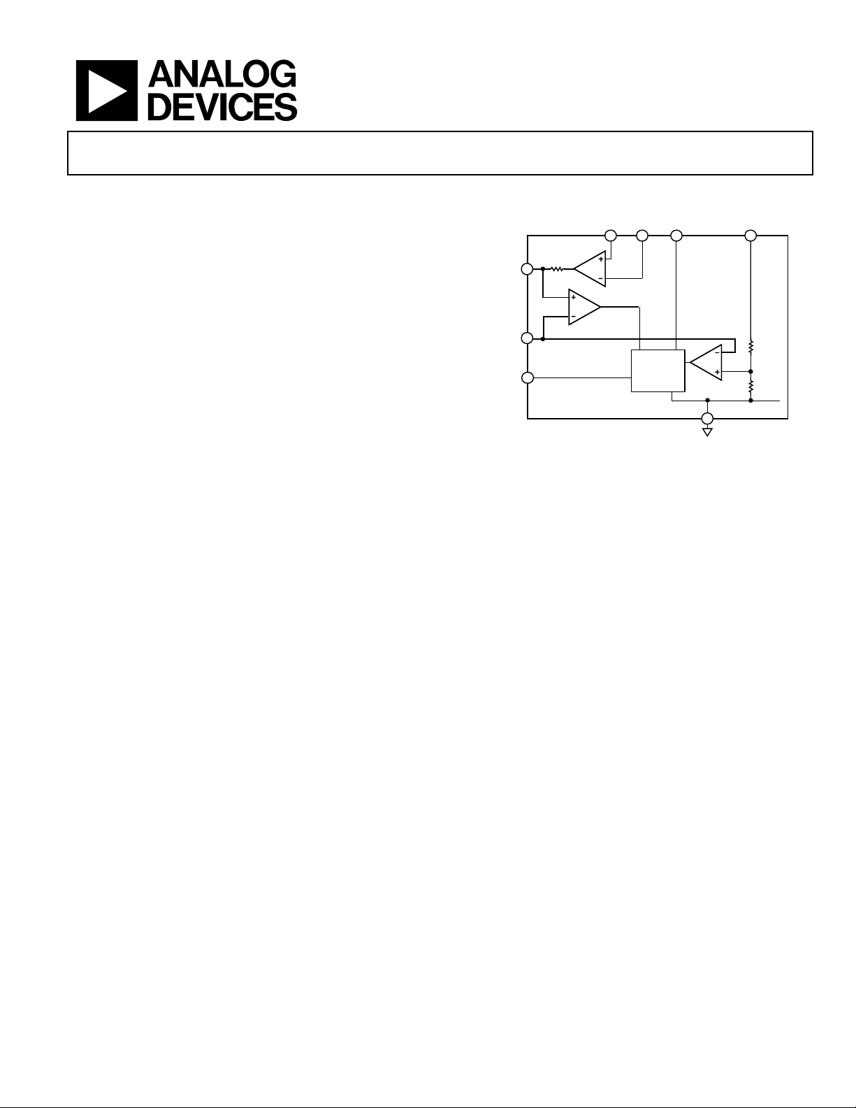
AD8240
FUNCTIONAL BLOCK DIAGRAM
V
P
L
U
S
SHUNT
BASE
6
LATCH-OFF
DRIVER
7
V
SENSE
REFERENCE
PWM
5
R
SENSE
1
10k
Ω
5V
2
3
AD8240
Figure 1.
PRODUCT HIGHLIGHTS
1. Partial LED lamp failure detection.
Allows for compliance with automotive regulations
for turn signal functionality detection and minimum
brightness, as well as running/brake light minimum
brightness compliance.
2. Current limiting/latch-off protection.
Limiting and latching off the LED current protects vehicle
wiring and prevents lamp damage
3. PWM input.
Provides brightness control.
4. Constant voltage output.
Saves cost by minimizing wiring and system design
complexity.
5. Drives an external transistor for low power operation.
Providing for an external power transistor allows the
AD8240 to be a low cost solution in a small package. A
more efficient design is made possible when the system
designer can select a power device with specifications
that match the application requirements.
6. Linear regulation.
Minimizes EMI, which allows faster system integration,
qualification, and time to market. Additionally, costs are
reduced by eliminating the inductor required for a
switching design. Because of the power-saving nature of
LED lamps as compared to incandescent lamps, a
switching driver is typically not required.
V
O
8
R1
350k
R2
250k
4
GND
Ω
Ω
04824-0-001
Rev. 0
Information furnished by Analog Devices is believed to be accurate and reliable.
However, no responsibility is assumed by Analog Devices for its use, nor for any
infringements of patents or other rights of third parties that may result from its use.
Specifications subject to change without notice. No license is granted by implication
or otherwise under any patent or patent rights of Analog Devices. Trademarks and
registered trademarks are the property of their respective owners.
One Technology Way, P.O. Box 9106, Norwood, MA 02062-9106, U.S.A.
Tel: 781.329.4700 www.analog.com
Fax: 781.326.8703 © 2004 Analog Devices, Inc. All rights reserved.
Page 2

AD8240
TABLE OF CONTENTS
Specifications..................................................................................... 3
Absolute Maximum Ratings............................................................ 4
Product Description ......................................................................... 5
Linear Regulator (Block A)......................................................... 5
High-Side Current-Sense Amplifier with Open LED
Detection (Block B)
Comparator with Latch-off OverCurrent Protection
(Block C)
Intelligent Driver (Block D)........................................................ 5
........................................................................................ 5
REVISION HISTORY
...................................................................... 5
Using/Evaluating the AD8240 LED Driver Monitor....................6
Setup................................................................................................6
Controlling the LED lamp............................................................7
Using/Evaluating the V
Advantages of Driving LED Lamps with Constant Voltage ........8
Background....................................................................................8
Monitoring the LEDs ....................................................................8
Driving Automotive LEDs............................................................8
Outline Dimensions....................................................................... 10
Ordering Guide .......................................................................... 11
Output.............................................7
Sense
4/04—Revision 0: Initial Version
Rev. 0 | Page 2 of 12
Page 3

AD8240
SPECIFICATIONS
TA = operating temperature range, V
Table 1.
Parameter Conditions Min Typ Max Unit
V
O
VO Regulation1 at 25°C V
VO Regulation2 -40°C to 125°C V
3
I
OUT
VO Rise Time I
V
Gain 24
SENSE
V
Accuracy −7 ±3 +7 %
SENSE
V
Output Impedance 8 10 12 kΩ
SENSE
Base Drive 15 mA
PWM Turn-On Threshold 3.5 V
PWM Turn-Off Threshold 1.4 V
V
Latch-Off Threshold4 0 0.1 0.3 V
SENSE
Latch-Off Delay
5
PWM Frequency Range DC 500 Hz
C
M
C
Range CL = 47 nF −30 +30 %
LOAD
Operating Current
V
Operating Range 9 27 V
PLUS
6
Shutdown Current PWM low 10 µA
5 V Reference Current 160 200 240 µA
Operating Temperature Range −40 +125 °C
1
VO = 12/5 of the applied reference voltage ±1% typical. Minimum V
2
VO = 12/5 of the applied reference voltage ±2% typical. Minimum V
3
The maximum output current level is set by the selection of the current shunt and power transistor.
4
(V
– 5 V Reference) The latch-off level is determined by the output level of the sense amplifier. When the amplifier output approaches 5 V, the output is latched off.
SENSE
This allows the maximum current output level to be determined by the shunt resistor value. Latch-off can be restored to on by cycling the PWM input off and back on.
5
Internal delay only. The external delay depends on the external capacitor values, LED string impedance, and wiring inductance.
6
This specifies V
only—ground current includes external transistor base drive.
PLUS
= 13.5 V, unless otherwise noted.
PLUS
5 V Reference = 5 V 12 V
= 13 V to 27 V −3 ±1 +3 %
PLUS
= 13 V to 27 V −6 ±2 +6 %
PLUS
R
= 0.4 Ω 500 mA
SHUNT
= 250 mA, CM = 22 nF, CL = 47 nF 12 µs
OUT
2 µs
22 nF
V
> 13 V 360 µA
PLUS
voltage for regulation depends on the external transistor Vbe and the shunt voltage.
PLUS
voltage for regulation depends on the external transistor Vbe and the shunt voltage.
PLUS
Rev. 0 | Page 3 of 12
Page 4

AD8240
ABSOLUTE MAXIMUM RATINGS
Table 2.
Parameters Rating
Supply Voltage, Continuous 27 V
Supply Voltage, Transient 30 V
Reverse Supply Protection −0.3 V
Operating Temperature 125°C
Storage Temperature −65°C to +150°C
Output Short-Circuit Duration1Indefinite
1
Output short circuits result in a latch-off condition.
ESD CAUTION
ESD (electrostatic discharge) sensitive device. Electrostatic charges as high as 4000 V readily accumulate on
the human body and test equipment and can discharge without detection. Although this product features
proprietary ESD protection circuitry, permanent damage may occur on devices subjected to high energy
electrostatic discharges. Therefore, proper ESD precautions are recommended to avoid performance
degradation or loss of functionality.
Stresses above those listed under Absolute Maximum Ratings
may cause permanent damage to the device. This is a stress
rating only; functional operation of the device at these or any
other conditions above those indicated in the operational
section of this specification is not implied. Exposure to absolute
maximum rating conditions for extended periods may affect
device reliability.
Rev. 0 | Page 4 of 12
Page 5

AD8240
PRODUCT DESCRIPTION
The AD8240 consists of four functional blocks labeled A
through D, as shown in Figure 2.
V
SENSE
REFERENCE
PWM
V
PLUS
B
C
5V
BASESHUNT
D
V
A
O
HIGH-SIDE CURRENT-SENSE AMPLIFIER WITH
OPEN LED DETECTION (BLOCK B)
This amplifier is used to measure the LED current by amplifying the voltage across a user-selected shunt resistor. It has a
gain of 24 and an overall accuracy of 5%. The output of the
amplifier is typically connected to a microcontroller A/D
converter input so that the condition of the LED lamp can be
determined. This output can also be tied to other devices such
as a latching comparator or output buffer. It is important to note
that the output of this amplifier has a relatively high impedance
of approximately 10 kΩ. As a result, a buffer amplifier should be
used if the load is less than 100 kΩ.
AD8240
GND
Figure 2. Simplified Functional Block Diagram
Table 3 briefly describes the blocks, while the sections that
follow provide more detailed information.
Table 3.
Block Description
A Linear regulator
B High-side current-sense amplifier
C Comparator
D Driver
LINEAR REGULATOR (BLOCK A)
The simplified architecture of the linear regulator block is an
amplifier and resistor divider. One input to the amplifier is
tied to the 5 V reference. The other input is tied to a resistor
divider that sets the ratio of the 5 V reference to V
result, the accuracy of the voltage output is proportional to
the accuracy of the 5 V reference. For example, if the 5 V
reference is 5% high (5.25 V), the output is 5% high (12.6 V).
. As a
O
04824-0-002
COMPARATOR WITH LATCH-OFF OVERCURRENT PROTECTION (BLOCK C)
This block is used to shut down the output in the case of a
short circuit or an overcurrent condition. When the output
of the high-side current-sense amplifier approaches 5 V, the
comparator output switches, causing the driver to latch off the
output voltage.
INTELLIGENT DRIVER (BLOCK D)
The intelligent driver provides multiple functions:
• Level shifts and conditions the output of the regulator
amplifier to drive an external user-selected power
transistor.
• Accepts PWM input so that LED brightness can be
controlled by a user-supplied PWM signal.
• The PWM input can also be used as a simple on/off
control for applications that do not require variable
brightness.
• Latch-off input that latches the output off when the
comparator trips during an overcurrent event. The latch
is reset by cycling the PWM input.
Rev. 0 | Page 5 of 12
Page 6

AD8240
≤
USING/EVALUATING THE AD8240 LED DRIVER MONITOR
Figure 3 shows a connection diagram for a typical application.
SETUP
In order to set up and evaluate the AD8240, the following
components and equipment are needed:
• A shunt resistor (typically 0.1 Ω to 0.5 Ω depending on the
load). See the Shunt Resistor Selection section.
• A transistor (the type depends on the load)
• Two capacitors
• LED load
• 5 V reference voltage
• 9 V to 27 V supply
• Oscilloscope
• Digital voltmeter (DVM)
Shunt Resistor Selection
The shunt resistor is chosen by the equation
SHUNT
For example if the load is expected to be 500 mA, the shunt
value should be equal to or less than 0.4 Ω. This keeps the
output of the current sense amplifier from being greater than
4.8 V in normal operation to prevent noise from causing the
output to latch off.
Circuit Configuration
Connect the pass transistor, capacitors, and LED load(s) as
shown in Figure 3. It is important to note that the value of CM
should be at least 22 nF to ensure circuit stability.
The LED lamp should be configured to expect 12 V. This is
the result of selecting the series/parallel combinations of LEDs
and series resistors. The series resistors can be used to adjust
for LED supplier brightness variations from lot to lot.
IR V2.0
LOAD
V
BATT
V
SENSE
REFERENCE
PWM
Connect 5 V to Pin 2 (5 V reference) and at least 9 V to Pin 5
(V
). It may be necessary to raise the V
PLUS
voltage to more
PLUS
than 13 V, depending on the drop across the pass transistor, for
the output to be regulated at 12 V. This varies according to the
application and the pass transistor type.
.
R
SHUNT
C
M
V
PLUS
SHUNT
5
R
SENSE
1
10k
Ω
5V
2
3
6
LATCH-OFF
DRIVER
7
BASE
22nF
V
O
8
R1
Ω
350k
R2
Ω
250k
CL
47nF
4
GND
04824-0-003
Figure 3. Connections for Typical Applications
Rev. 0 | Page 6 of 12
Page 7

AD8240
CONTROLLING THE LED LAMP
The LEDs are turned on and off depending on the CMOS
compatible digital voltage level present at the PWM pin (Pin 3).
This voltage can be continuous for a simple on/off function, or
PWM for dimming control. The PWM frequency should be less
than 500 Hz with a range from 5% to 100%. Typical values are
5% for running and 95% for braking.
USING/EVALUATING THE V
Important: The output impedance of V
OUTPUT
SENSE
SENSE
is approximately
10 kΩ. Because of this, it may be necessary to buffer the output
in order to drive a load of less than 100 kΩ. An oscilloscope,
micro-controller A/D converter, or DVM may be used to
accurately measure the voltage at the V
The V
output is used to detect a partial LED failure, or an
SENSE
overcurrent condition. The voltage present at V
SENSE
pin.
is propor-
SENSE
tional to the current through the load with the equation
I
LOAD
= (V
SENSE
/24)/R
SHUNT
Selection of the shunt resistor can be found by manipulating this
equation.
For example
V
= I
SENSE
LOAD
× R
SHUNT
To determine if the load is correct, the voltage at V
be as follows during full power operation:
500 mA × 0.4 Ω × 24 V/V = 4.8 V
If there is a partial LED failure, V
drops in proportion to the
SENSE
quantity of the failure. For example, if 25% of the LEDs fail, the
voltage drops by 25%.
If there is a short to ground, V
is near 0 V because the
SENSE
output is latched off and no current is flowing.
Using/Evaluating the Short-Circuit Protection Feature
If there is a short or an overload condition, the voltage at
V
falls close to zero, and the output shuts down
SENSE
(the transistor driver shuts off). This resets when the PWM
voltage is brought low and then high again. If the condition
persists, the AD8240 attempts to drive the output to 12 V and
then immediately shuts down. If a PWM voltage is used, the
AD8240 attempts to start after each PWM cycle.
This can be simulated by increasing the load so the voltage at
V
slightly exceeds 5 V. When this happens, the output shuts
SENSE
down, and the V
voltage is close to 0 V.
SENSE
SENSE
should
Expected Load = 500 mA
R
= 0.4 Ω
SHUNT
Rev. 0 | Page 7 of 12
Page 8

AD8240
ADVANTAGES OF DRIVING LED LAMPS WITH CONSTANT VOLTAGE
The advantages of driving LED lamps with constant voltage are
Low system cost
•
Accurate monitoring
•
Proven strategy
•
BACKGROUND
A great variety of LED lamps are being used in automotive
applications. The most popular application is center brake
lamps. Currently, many manufacturers are developing
technology to use LEDs for left/right brake lamps, running
lamps, and turn signals. There are also plans to use high power
LEDs for forward lighting fog lamps and low beams.
There are two fundamental types of LEDs used in these applications. The first is the low power bright LED. The second type is
the high power, extremely bright LED in the 1 W to 10 W range.
While the following information can be applied to applications
using the high power LED, or incandescent lamps, the constant
voltage method is designed for applications typically using the
low power bright LEDs. This type of LED is used in arrays that
form LED lamps.
MONITORING THE LEDS
In addition to driving the LED lamp, the electronics in the
control module must include a method for monitoring partial
LED failure in the lamp. Certain factors, such as overdriving
and mechanical stress, can cause LED failures.
Auto manufacturers are using LED lamps as a way to differentiate themselves and give a car a unique appearance. Several
failed LEDs in the lamp would ruin the aesthetics of the lamp.
As a result, manufacturers are demanding the ability to monitor
the LED lamps for partial failure.
In addition to monitoring the LEDs for aesthetic reasons,
monitoring must also be included as a result of automotive
regulations. These regulations specify the minimum light
output of external lamps. For example, if half of the LEDs in
a particular lamp failed, the lamp would still operate, but the
light output would be insufficient to meet automotive
regulations for brightness. This concern is not an issue for
incandescent bulbs, because they are either completely on or
completely off. The ability of the LED lamp to provide some
light output in the case of partial outage, however, allows for an
extra degree of safety over incandescent lamps. Additionally,
there are automotive regulations requiring the monitoring of
the turn signals regardless of the type of light source.
DRIVING AUTOMOTIVE LEDS
There are two different architectures for driving LEDs in
left/right/center brake lamps, running lamps, and turn signals.
Constant Current
The most common method for driving LEDs is with a constant
current. This current can be supplied from a constant current
source or from a constant voltage source in series with a ballast
resistor. Driving LEDs without some form of ballast carries
some risk of premature LED failure due to thermal runaway in
high temperature ambient conditions.
For example, in the simplest application, the center brake lamp
is driven from a relatively constant voltage with brightness
controlled by a series ballast resistor. This simple driving
method has been used in a wide variety of automotive platforms
for some time. With this method, the LEDs and ballast resistors
are preselected for brightness as part of the manufacturing
strategy.
When driving with a constant current source, LED driving
and monitoring cannot be done using two or fewer wires
(shared ground). Since the current is constant, it does not
change with partial LED failure. Instead, the current is divided
among the remaining functional LEDs, causing them to fail
prematurely at an unpredictable rate. Additionally, it is not
possible to detect partial failure by measuring the voltage
change. The voltage does not change by a detectable amount
because of the steep V/I curve exhibited by bright LEDs. When
using a constant current scheme, at least one additional wire
per lamp must be added to the harness to monitor partial or
total LED failure. Additionally, electronic modules must be
added to each lamp.
Constant Voltage
Driving LEDs with a constant voltage allows for easy, low cost
detection of partial failure, an advantage not available with a
constant-current architecture. This is because the current from
the voltage source changes in direct proportion to the number
of LEDs that have failed. This current can be measured with a
low cost shunt and an amplifier back at the body control
module. This detection scheme is implemented in the AD8240
LED driver/monitor through the use of a high-side, currentsensing amplifier. The current is measured on the high side in
order to separate the current from those combined in the
chassis ground return or shared-wire ground return.
Rev. 0 | Page 8 of 12
Page 9

AD8240
As a result, the constant voltage driving/monitoring method is
the lowest cost and least-prone-to-failure method for driving
and monitoring LEDs from a system perspective. This is
primarily because the number of wires and connections can be
minimized. By using a constant voltage driver and measuring
the current, an LED lamp can be driven
only two wires (power and ground). In many cases, this can be
reduced to one wire when the chassis or shared ground return
is used. This is a similar architecture used with incandescent
bulbs, which means no changes to the wiring harness are
necessary with this LED implementation.
Most automotive platforms no longer use a switch on the
dashboard to directly control the incandescent lamps. These
lamps are now controlled and driven by the body control ECU.
By using this constant voltage architecture, the control and drive
function for the LEDs can remain in the ECU with minimal
design modification.
and monitored using
Constant voltage driving/monitoring is a proven method
already in use in a number of automotive platforms to drive
LED tail, running, and turn-indicator lamps.
The AD8240 LED lamp driver/monitor is designed for use in
the body control or related module. When used this way, it is
very similar to the method that has been used to control
external incandescent lamps. By utilizing the existing lamp
driving architecture, additional modules are not required to
drive the external lamps, which further minimizes the cost.
It is possible to retrofit existing lamp driving modules with
the AD8240 with minimal engineering time required.
Rev. 0 | Page 9 of 12
Page 10

AD8240
OUTLINE DIMENSIONS
3.00
BSC
85
3.00
BSC
PIN 1
0.65 BSC
0.15
0.00
0.38
0.22
COPLANARITY
0.10
COMPLIANT TO JEDEC STANDARDS MO-187AA
4
SEATING
PLANE
4.90
BSC
1.10 MAX
0.23
0.08
8°
0°
0.80
0.60
0.40
Figure 4. 8-Lead Mini Small Outline Package [MSOP]
(RM-8)
Dimensions shown in millimeters
Rev. 0 | Page 10 of 12
Page 11

AD8240
ORDERING GUIDE
Model Temperature Range Package Description Package Option Package Outline
AD8240YRM −40°C to +125°C 8-Lead MSOP RM-8 JTA
AD8240YRM-REEL −40°C to +125°C MSOP, 13” Tape and Reel RM-8 JTA
AD8240YRM-REEL7 −40°C to +125°C MSOP, 7” Tape and Reel RM-8 JTA
Rev. 0 | Page 11 of 12
Page 12

AD8240
NOTES
© 2004 Analog Devices, Inc. All rights reserved. Trademarks and
registered trademarks are the property of their respective owners.
D04824-0-4/04(0)
Rev. 0 | Page 12 of 12
 Loading...