

Page 1
Single Supply, Rail-to-Rail
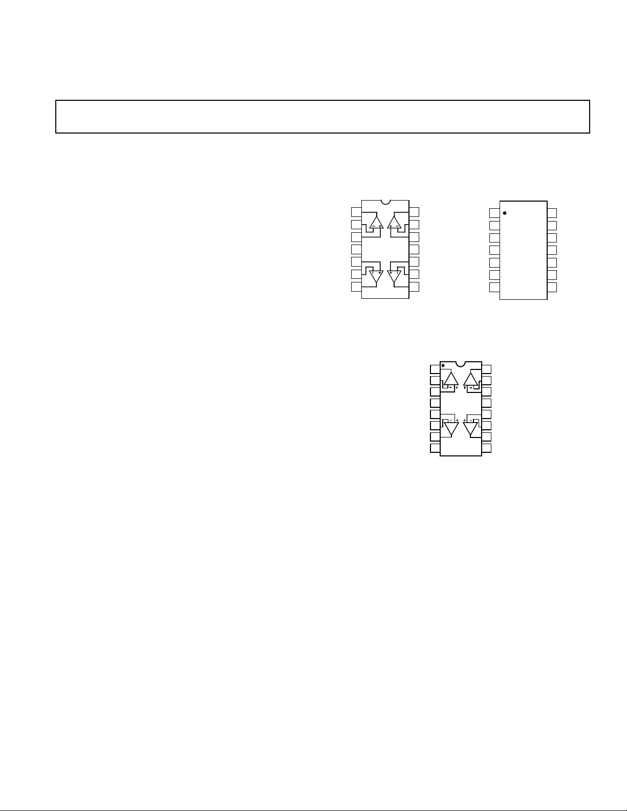
OUT A
–IN A
OUT D
–IN D
+INB
–INB
OUTB
+IN C
–IN C
OUT C
+IN A
V+
+IN D
V–
1
2
14
13
5
6
7
10
9
8
3
4
12
11
TOP VIEW
(Not to Scale)
AD824
OUT A
–IN A
OUT D
–IN D
+IN B
–IN B
OUT B
+IN C
–IN C
OUT C
+IN A
V+
+IN D
V–
1
2
14
13
5
6
7
10
9
8
3
4
12
11
TOP VIEW
AD824
1
2
3
4
5
6
7
8
14
13
12
11
10
9
15
16
OUT A
–IN A
+IN A
V+
+IN B
–IN B
OUT B
–IN D
+IN D
V–
+IN C
–IN C
OUT C
OUT D
NC
NC
NC = NO CONNECT
AD824
a
FEATURES
Single Supply Operation: 3 V to 30 V
Very Low Input Bias Current: 2 pA
Wide Input Voltage Range
Rail-to-Rail Output Swing
Low Supply Current: 500 mA/Amp
Wide Bandwidth: 2 MHz
Slew Rate: 2 V/ms
No Phase Reversal
APPLICATIONS
Photo Diode Preamplifier
Battery Powered Instrumentation
Power Supply Control and Protection
Medical Instrumentation
Remote Sensors
Low Voltage Strain Gage Amplifiers
DAC Output Amplifier
GENERAL DESCRIPTION
The AD824 is a quad, FET input, single supply amplifier, featuring rail-to-rail outputs. The combination of FET inputs and
rail-to-rail outputs makes the AD824 useful in a wide variety of
low voltage applications where low input current is a primary
consideration.
The AD824 is guaranteed to operate from a 3 V single supply
up to ±15 volt dual supplies.
Fabricated on ADI’s complementary bipolar process, the AD824
has a unique input stage that allows the input voltage to safely
extend beyond the negative supply and to the positive supply
without any phase inversion or latchup. The output voltage
swings to within 15 millivolts of the supplies. Capacitive loads
to 350 pF can be handled without oscillation.
The FET input combined with laser trimming provides an input
that has extremely low bias currents with guaranteed offsets below 300 µV. This enables high accuracy designs even with high
source impedances. Precision is combined with low noise,
making the AD824 ideal for use in battery powered medical
equipment.
Low Power, FET-Input Op Amp
AD824
PIN CONFIGURATIONS
14-Lead Epoxy DIP
(N Suffix)
16-Lead Epoxy SO
(R Suffix)
Applications for the AD824 include portable medical equipment,
photo diode preamplifiers and high impedance transducer
amplifiers.
The ability of the output to swing rail-to-rail enables designers
to build multistage filters in single supply systems and maintain
high signal-to-noise ratios.
The AD824 is specified over the extended industrial (–40°C to
+85°C) temperature range and is available in 14-pin DIP and
narrow 14-pin and 16-pin SO packages.
14-Lead Epoxy SO
(R Suffix)
REV. A
Information furnished by Analog Devices is believed to be accurate and
reliable. However, no responsibility is assumed by Analog Devices for its
use, nor for any infringements of patents or other rights of third parties
which may result from its use. No license is granted by implication or
otherwise under any patent or patent rights of Analog Devices.
One Technology Way, P.O. Box 9106, Norwood, MA 02062-9106, U.S.A.
Tel: 617/329-4700 World Wide Web Site: http://www.analog.com
Fax: 617/326-8703 © Analog Devices, Inc., 1997
Page 2

AD824–SPECIFICATIONS
ELECTRICAL SPECIFICATIONS
(@ VS = +5.0 V, VCM = 0 V, V
= 0.2 V, TA = +258C unless otherwise noted)
OUT
Parameter Symbol Conditions Min Typ Max Units
INPUT CHARACTERISTICS
Offset Voltage AD824A V
Offset Voltage AD824B V
Input Bias Current I
Input Offset Current I
B
OS
OS
OS
T
to T
MIN
T
MIN
T
MIN
T
MIN
to T
to T
to T
MAX
MAX
MAX
MAX
0.1 1.0 mV
1.5 mV
300 µV
900 µV
212pA
300 4000 pA
210pA
300 pA
Input Voltage Range –0.2 3.0 V
Common-Mode Rejection Ratio CMRR V
Input Impedance 10
Large Signal Voltage Gain A
VO
= 0 V to 2 V 66 80 dB
CM
V
= 0 V to 3 V 60 74 dB
CM
T
MIN
to T
MAX
60 dB
13
i3.3 ΩipF
VO = 0.2 V to 4.0 V
R
= 2 kΩ 20 40 V/mV
L
R
= 10 kΩ 50 100 V/mV
L
R
= 100 kΩ 250 1000 V/mV
L
T
MIN
to T
= 100 kΩ 180 400 V/mV
MAX, RL
Offset Voltage Drift ∆VOS/∆T2µV/°C
OUTPUT CHARACTERISTICS
Output Voltage High V
Output Voltage Low V
Short Circuit Limit I
Open-Loop Impedance Z
OH
OL
SC
OUT
I
= 20 µA 4.975 4.988 V
SOURCE
to T
T
MIN
I
SOURCE
T
MIN
I
SINK
T
MIN
I
SINK
T
MIN
MAX
= 2.5 mA 4.80 4.85 V
to T
MAX
= 20 µA1525mV
to T
MAX
= 2.5 mA 120 150 mV
to T
MAX
4.97 4.985 V
4.75 4.82 V
20 30 mV
140 200 mV
Sink/Source ±12 mA
T
MIN
to T
MAX
±10 mA
f = 1 MHz, AV = 1 100 Ω
POWER SUPPLY
Power Supply Rejection Ratio PSRR VS = 2.7 V to 12 V 70 80 dB
Supply Current/Amplifier I
to T
T
MIN
SY
T
MIN
to T
MAX
MAX
66 dB
500 600 µA
DYNAMIC PERFORMANCE
Slew Rate SR RL = 10 kΩ, AV = 1 2 V/µs
Full-Power Bandwidth BW
Settling Time t
S
P
1% Distortion, VO = 4 V p-p 150 kHz
V
= 0.2 V to 4.5 V, to 0.01% 2.5 µs
OUT
Gain Bandwidth Product GBP 2 MHz
Phase Margin φo No Load 50 Degrees
Channel Separation CS f = 1 kHz, RL = 2 kΩ –123 dB
NOISE PERFORMANCE
Voltage Noise en p-p 0.1 Hz to 10 Hz 2 µV p-p
Voltage Noise Density e
Current Noise Density i
n
n
f = 1 kHz 16 nV/√Hz
f = 1 kHz 0.8 fA/√Hz
Total Harmonic Distortion THD f = 10 kHz, RL = 0, AV = +1 0.005 %
–2–
REV. A
Page 3

AD824
ELECTRICAL SPECIFICATIONS
(@ VS = 615.0 V, V
= 0 V, TA = +258C unless otherwise noted)
OUT
Parameter Symbol Conditions Min Typ Max Units
INPUT CHARACTERISTICS
Offset Voltage AD824A V
Offset Voltage AD824B V
Input Bias Current I
Input Bias Current I
Input Offset Current I
B
B
OS
OS
OS
T
to T
MIN
T
MIN
to T
MAX
MAX
VCM = 0 V 4 35 pA
T
to T
MIN
MAX
VCM = –10 V 25 pA
T
to T
MIN
MAX
0.5 2.5 mV
0.6 4.0 mV
0.5 1.5 mV
0.6 2.5 mV
500 4000 pA
320 pA
500 pA
Input Voltage Range –15 13 V
Common-Mode Rejection Ratio CMRR V
Input Impedance 10
Large Signal Voltage Gain A
VO
= –15 V to 13 V 70 80 dB
CM
T
MIN
to T
MAX
66 dB
13
i3.3 ΩipF
Vo = –10 V to +10 V;
R
= 2 kΩ 12 50 V/mV
L
R
= 10 kΩ 50 200 V/mV
L
R
= 100 kΩ 300 2000 V/mV
L
T
MIN
to T
= 100 kΩ 200 1000 V/mV
MAX, RL
Offset Voltage Drift ∆VOS/∆T2µV/°C
OUTPUT CHARACTERISTICS
Output Voltage High V
Output Voltage Low V
Short Circuit Limit I
Open-Loop Impedance Z
OH
OL
SC
OUT
I
= 20 µA 14.975 14.988 V
SOURCE
T
to T
MIN
I
SOURCE
T
MIN
I
SINK
T
MIN
I
SINK
T
MIN
Sink/Source, T
f = 1 MHz, A
MAX
= 2.5 mA 14.80 14.85 V
to T
MAX
= 20 µA –14.985 –14.975 V
to T
MAX
= 2.5 mA –14.88 –14.85 V
to T
MAX
to T
MIN
= 1 100 Ω
V
MAX
14.970 14.985 V
14.75 14.82 V
–14.98 –14.97 V
–14.86 –14.8 V
±8 ±20 mA
POWER SUPPLY
Power Supply Rejection Ratio PSRR V
Supply Current/Amplifier I
SY
= 2.7 V to 15 V 70 80 dB
S
T
to T
MIN
V
O
T
MIN
MAX
= 0 V 560 625 µA
to T
MAX
68 dB
675 µA
DYNAMIC PERFORMANCE
Slew Rate SR R
Full-Power Bandwidth BW
Settling Time t
P
S
= 10 kΩ, AV = 1 2 V/µs
L
1% Distortion, VO = 20 V p-p 33 kHz
V
= 0 V to 10 V, to 0.01% 6 µs
OUT
Gain Bandwidth Product GBP 2 MHz
Phase Margin φo 50 Degrees
Channel Separation CS f = 1 kHz, R
=2 kΩ –123 dB
L
NOISE PERFORMANCE
Voltage Noise e
Voltage Noise Density e
Current Noise Density i
Total Harmonic Distortion THD f =10 kHz, V
p-p 0.1 Hz to 10 Hz 2 µV p-p
n
n
n
f = 1 kHz 16 nV/√Hz
f = 1 kHz 1.1 fA/√Hz
= 3 V rms,
R
= 10 kΩ 0.005 %
L
O
REV. A
–3–
Page 4

AD824–SPECIFICATIONS
ELECTRICAL SPECIFICATIONS
(@ VS = +3.0 V, VCM = 0 V, V
= 0.2 V, TA = +258C unless otherwise noted)
OUT
Parameter Symbol Conditions Min Typ Max Units
INPUT CHARACTERISTICS
Offset Voltage AD824A -3 V V
Input Bias Current I
Input Offset Current I
B
OS
OS
T
to T
MIN
T
MIN
T
MIN
to T
to T
MAX
MAX
MAX
0.2 1.0 mV
1.5 mV
212pA
250 4000 pA
210pA
250 pA
Input Voltage Range 0 1 V
Common-Mode Rejection Ratio CMRR V
Input Impedance 10
Large Signal Voltage Gain A
VO
= 0 V to 1 V 58 74 dB
CM
T
MIN
to T
MAX
56 dB
13
i3.3 ΩipF
VO = 0.2 V to 2.0 V
R
= 2 kΩ 10 20 V/mV
L
R
= 10 kΩ 30 65 V/mV
L
R
= 100 kΩ 180 500 V/mV
L
T
MIN
to T
= 100 kΩ 90 250 V/mV
MAX, RL
Offset Voltage Drift ∆VOS/∆T2µV/°C
OUTPUT CHARACTERISTICS
Output Voltage High V
Output Voltage Low V
Short Circuit Limit I
Short Circuit Limit I
Open-Loop Impedance Z
OH
OL
SC
SC
OUT
I
T
I
T
I
T
I
T
= 20 µA 2.975 2.988 V
SOURCE
to T
MIN
SOURCE
MIN
SINK
MIN
SINK
MIN
MAX
= 2.5 mA 2.8 2.85 V
to T
MAX
= 20 µA1525mV
to T
MAX
= 2.5 mA 120 150 mV
to T
MAX
2.97 2.985 V
2.75 2.82 V
20 30 mV
140 200 mV
Sink/Source ±8mA
Sink/Source, T
f = 1 MHz, A
to T
MIN
= 1 100 Ω
V
MAX
±6mA
POWER SUPPLY
Power Supply Rejection Ratio PSRR V
Supply Current/Amplifier I
SY
= 2.7 V to 12 V, 70 dB
S
T
to T
MIN
MAX
VO = 0.2 V, T
MIN
to T
MAX
66 dB
500 600 µA
DYNAMIC PERFORMANCE
Slew Rate SR R
Full-Power Bandwidth BW
Settling Time t
P
S
=10 kΩ, AV = 1 2 V/µs
L
1% Distortion, VO = 2 V p-p 300 kHz
V
= 0.2 V to 2.5 V, to 0.01% 2 µs
OUT
Gain Bandwidth Product GBP 2 MHz
Phase Margin φo 50 Degrees
Channel Separation CS f = 1 kHz, R
= 2 kΩ –123 dB
L
NOISE PERFORMANCE
Voltage Noise e
Voltage Noise Density e
Current Noise Density i
p-p 0.1 Hz to 10 Hz 2 µV p-p
n
n
n
f = 1 kHz 16 nV/√Hz
0.8 fA/√Hz
Total Harmonic Distortion THD f = 10 kHz, RL = 0, AV = +1 0.01 %
–4–
REV. A
Page 5
AD824
WARNING!
ESD SENSITIVE DEVICE
I6
R1 R2
R9
R7
R17
R14
R12
R13
R15
V
CC
I5
Q18 Q29
Q27Q21
Q20
Q23
Q25Q24
Q31
Q28
Q22
Q19
Q7
Q6
Q5
Q8
Q3
Q2
Q4
I1 I2 I3
I4
+IN
J1
–IN
C1
Q26
V
OUT
J2
V
EE
C3
C2
C4
WAFER TEST LIMITS
(@ VS = +5.0 V, VCM = 0 V, TA = +258C unless otherwise noted)
Parameter Symbol Conditions Limit Units
Offset Voltage V
Input Bias Current I
Input Offset Current I
Input Voltage Range V
OS
B
OS
CM
Common-Mode Rejection Ratio CMRR V
= 0 V to 2 V 66 dB min
CM
1.0 mV max
12 pA max
20 pA
–0.2 to 3.0 V min
Power Supply Rejection Ratio PSRR V = + 2.7 V to +12 V 70 µV/V
Large Signal Voltage Gain A
Output Voltage High V
Output Voltage Low V
Supply Current/Amplifier I
NOTE
Electrical tests and wafer probe to the limits shown. Due to variations in assembly
methods and normal yield loss, yield after packaging is not guaranteed for
standard product dice. Consult factory to negotiate specifications based on dice
lot qualifications through sample lot assembly and testing.
ABSOLUTE MAXIMUM RATINGS
1
VO
OH
OL
SY
R
= 2 kΩ 15 V/mV min
L
I
= 20 µA 4.975 V min
SOURCE
I
= 20 µA 25 mV max
SINK
VO = 0 V, R
= ∞ 600 µA max
L
DICE CHARACTERISTICS
Supply Voltage . . . . . . . . . . . . . . . . . . . . . . . . . . . . . . . . ±18 V
Input Voltage . . . . . . . . . . . . . . . . . . . . . . . –V
– 0.2 V to +V
S
S
Differential Input Voltage . . . . . . . . . . . . . . . . . . . . . . . ±30 V
Output Short Circuit Duration to GND . . . . . . . . . Indefinite
Storage Temperature Range
N, R Package . . . . . . . . . . . . . . . . . . . . . . –65°C to +150°C
Operating Temperature Range
AD824A, B . . . . . . . . . . . . . . . . . . . . . . . . –40°C to +85°C
Junction Temperature Range
N, R Package . . . . . . . . . . . . . . . . . . . . . . –65°C to +150°C
Lead Temperature Range (Soldering, 60 sec) . . . . . . . +300°C
Package Type θ
2
JA
θ
JC
Units
AD824 Die Size 0.70 X 0.130 inch, 9,100 sq. mils.
Substrate (Die Backside) Is Connected to V+. Transistor
Count, 143.
14-Pin Plastic DIP (N) 76 33 °C/W
14-Pin SOIC (R) 120 36 °C/W
16-Pin SOIC (R) 92 27 °C/W
NOTES
1
Absolute maximum ratings apply to both DICE and packaged parts unless
otherwise noted.
2
θJA is specified for the worst case conditions, i.e., θ
for P-DIP packages; θJA is specified for device soldered in circuit board for SOIC
package.
is specified for device in socket
JA
ORDERING GUIDE
Temperature
Model Range Package Option
AD824AN –40°C to +85°C 14-Pin Plastic DIP
AD824BN –40°C to +85°C 14-Pin Plastic DIP
AD824AR –40°C to +85°C 14-Pin SOIC
AD824AR-3V –40°C to +85°C 14-Pin SOIC
AD824AN-3V –40°C to +85°C 14-Pin Plastic DIP
AD824AR-14 –40°C to +85°C 14-Pin SOIC
AD824AR-14-3V –40°C to +85°C 14-Pin SOIC
AD824AR-16 –40°C to +85°C 16-Pin SOIC
AD824AChips +25°C DICE
CAUTION
ESD (electrostatic discharge) sensitive device. Electrostatic charges as high as 4000 V readily
accumulate on the human body and test equipment and can discharge without detection.
Although the AD824 features proprietary ESD protection circuitry, permanent damage may
occur on devices subjected to high energy electrostatic discharges. Therefore, proper ESD
precautions are recommended to avoid performance degradation or loss of functionality.
REV. A –5–
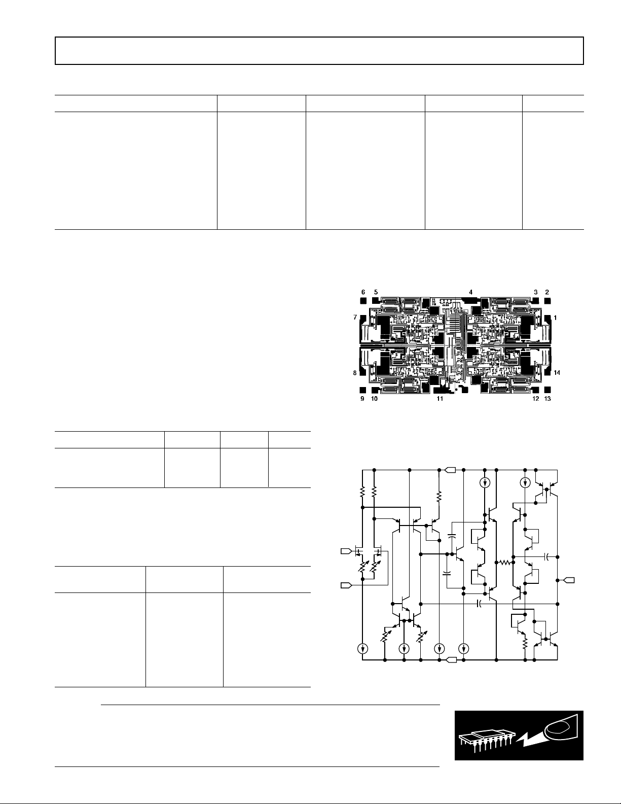
Figure 1. Simplified Schematic of 1/4 AD824
Page 6

AD824–Typical Characteristics
100 10M1k 10k 100k 1M
80
60
40
20
0
GAIN – dB
180
135
90
45
PHASE – Degrees
VS = +5V
NO LOAD
10M1k 10k 100k 1M
60
40
20
0
–20
GAIN – dB
180
135
90
45
PHASE – Degrees
VS = +5V
C
L
= 220pF
10
0%
100
90
1µs50mV
80
60
40
GAIN – dB
20
0
100 10M1k 10k 100k 1M
100
90
10
0%
VS = ±15V
NO LOAD
45
90
135
180
1µs50mV
Figure 2. Open-Loop Gain/Phase and Small Signal
Response, V
= ±15 V, No Load
S
PHASE – Degrees
100
90
10
0%
1µs50mV
Figure 4. Open-Loop Gain/Phase and Small Signal
Response, V
= +5 V, No Load
S
80
60
40
GAIN – dB
20
0
100 10M1k 10k 100k 1M
100
90
10
0%
Figure 3. Open-Loop Gain/Phase and Small Signal
Response, V
= ±15 V, CL = 100 pF
S
1µs50mV
VS = ±15V
C
= 100pF
L
45
90
135
180
PHASE – Degrees
–6–
Figure 5. Open-Loop Gain/Phase and Small Signal
Response, V
= +5 V, CL = 220 pF
S
REV. A
Page 7

AD824
60
40
20
GAIN – dB
0
–20
9.950
2µs5V
2µs5V
µs
µs
VS = +3V
NO LOAD
45
90
135
180
PHASE – Degrees
10M1k 10k 100k 1M
100
90
10
0%
1µs50mV
100
90
10
0%
100
90
10
0%
Figure 8. Slew Rate, RL = 10k
t
t
10.810
Figure 6. Open-Loop Gain/Phase and Small Signal
Response, V
60
40
20
GAIN – dB
0
–20
= +3 V, No Load
S
100
90
10
0%
1µs50mV
VS = +3V
C
= 220pF
L
45
90
135
180
10M1k 10k 100k 1M
Figure 9. Phase Reversal with Inputs Exceeding Supply by
1 Volt
PHASE – Degrees
100
90
V
OUT
10
0%
5V
0.8
0.7
0.6
0.5
0.4
0.3
OUTPUT TO RAIL – Volts
0.2
0.1
0
1µ 10m5µ 10µ 50µ 100µ 500µ 1m 5m
LOAD CURRENT – A
100µs
SOURCE
SINK
Figure 7. Open-Loop Gain/Phase and Small Signal
Response, V
= +3 V, CL = 220 pF
S
REV. A
Figure 10. Output Voltage to Supply Rail vs. Sink and
Source Load Currents
–7–
Page 8

AD824–Typical Characteristics
TEMPERATURE – °C
150
–25
–60 140–40 –20 0 20 40 60 80 100 120
125
100
75
50
25
0
INPUT OFFSET CURRENT – pA
VS = 5, 0
INPUT BIAS CURRENT – pA
TEMPERATURE – °C
100k
20 14040 60 80 100 120
10k
1k
100
10
1
VS = 5, 0
14
COUNT = 60
12
60
40
20
NOISE DENSITY – nV/√Hz
5 10 15 20
+3V ≤ VS ≤ ±15V
FREQUENCY – kHz
Figure 11. Voltage Noise Density
0.1
0.010
THD+N – %
0.001
VS = +3
VS = +5
VS = ±15
RL = 0
A
= +1
V
10
8
6
NUMBER OF UNITS
4
2
0
–2.5 2.5–2.0 –1.5 –1.0 –0.5 0 0.5 1.0 1.5 2.0
OFFSET VOLTAGE DRIFT
Figure 14. TC VOS Distribution, –55°C to +125°C, VS = 5, 0
0.0001
280
240
200
160
120
NUMBER OF UNITS
80
40
0
–0.5 0.5–0.4 –0.3 –0.2 –0.1 0 0.1 0.2 0.3 0.4
Figure 13. Input Offset Distribution, VS = 5, 0
20 100 1k 10k 20k
FREQUENCY – Hz
Figure 12. Total Harmonic Distortion
COUNT = 860
OFFSET VOLTAGE – mV
Figure 15. Input Offset Current vs. Temperature
Figure 16. Input Bias Current vs. Temperature
–8–
REV. A
Page 9

AD824
FREQUENCY – Hz
120
0
10 10M100
POWER SUPPLY REJECTION – dB
1k 10k 100k 1M
100
80
60
40
20
120
100
80
60
40
20
COMMON-MODE REJECTION – dB
0
10 10M100 1k 10k 100k 1M
FREQUENCY – Hz
Figure 17. Common-Mode Rejection vs. Frequency
–40
–60
...
1k
100
10
INPUT VOLTAGE NOISE – nV/√Hz
1
1 100k10 100 1k 10k
FREQUENCY – Hz
Figure 20. Input Voltage Noise Spectral Density vs.
Frequency
–80
THD – dB
–100
–120
100 100k1k 10k
Figure 18. THD vs. Frequency, 3 V rms
100
80
60
40
20
OPEN-LOOP GAIN – dB
0
–20
10 10M100
FREQUENCY – Hz
±15V
+3, 0V
1k 10k 100k 1M
FREQUENCY – Hz
100
80
60
40
20
PHASE MARGIN – Degrees
0
–20
Figure 21. Power Supply Rejection vs. Frequency
30
25
20
15
10
OUTPUT VOLTAGE – Volts
5
0
1k 1M3k
10k 30k 100k 300k
INPUT FREQUENCY – Hz
Figure 19. Open-Loop Gain and Phase vs. Frequency
REV. A –9–
Figure 22. Large Signal Frequency Response
Page 10

AD824
10
0%
100
90
5µs5V
–80
–90
–100
–110
–120
CROSSTALK – dB
–130
–140
10 100
FREQUENCY – Hz
1 TO 4
1 TO 2
1k 10k 100k
Figure 23. Crosstalk vs. Frequency
10k
1k
100
10
1
OUTPUT IMPEDANCE – Ω
.1
1 TO 3
Figure 26. Large Signal Response
2750
2500
2250
2000
1750
1500
SUPPLY CURRENT – µA
1250
VS = ±15V
VS = 3, 0
.01
10 10M100
1k 10k 100k 1M
FREQUENCY – Hz
Figure 24. Output Impedance vs. Frequency, Gain = +1
500ns20mV
100
90
10
0%
Figure 25. Small Signal Response, Unity Gain Follower,
i
100 pF Load
10k
1000
–60 140–40
–20 0 20 40 60 80 100 120
TEMPERATURE – °C
Figure 27. Supply Current vs. Temperature
1000
VS = ±15V
V
= 3, 0
S
100
V
– V
OL
S
10
OUTPUT SATURATION VOLTAGE – mV
0
0.01 10.00.10 1.0
VS – V
OH
LOAD CURRENT – mA
Figure 28. Output Saturation Voltage
–10–
REV. A
Page 11

AD824
8
4
0.01µF
20pF
20kΩ
100Ω
V
OUT
+V
S
–V
S
0.01µF
C
L
1/4
AD824
V
I
N
APPLICATION NOTES
INPUT CHARACTERISTICS
In the AD824, n-channel JFETs are used to provide a low
offset, low noise, high impedance input stage. Minimum input
common-mode voltage extends from 0.2 V below –V
than +V
. Driving the input voltage closer to the positive rail will
S
to 1 V less
S
cause a loss of amplifier bandwidth.
The AD824 does not exhibit phase reversal for input voltages up
to and including +V
AD824 voltage follower to a 0 V to +5 V (+V
. Figure 29a shows the response of an
S
) square wave in-
S
put. The input and output are superimposed. The output tracks
the input up to +V
without phase reversal. The reduced band-
S
width above a 4 V input causes the rounding of the output wave
form. For input voltages greater than +V
, a resistor in series
S
with the AD824’s noninverting input will prevent phase reversal
at the expense of greater input voltage noise. This is illustrated
in Figure 29b.
2µs1V
100
90
10
GND
0%
1V
(a)
10µs1V
+V
GND
1V
100
90
S
10
0%
1V
(b)
R
P
V
IN
+5V
V
OUT
A current-limiting resistor should be used in series with the input of the AD824 if there is a possibility of the input voltage exceeding the positive supply by more than 300 mV or if an input
voltage will be applied to the AD824 when ± V
= 0. The ampli-
S
fier will be damaged if left in that condition for more than 10
seconds. A 1 kΩ resistor allows the amplifier to withstand up to
10 volts of continuous overvoltage and increases the input voltage noise by a negligible amount.
Input voltages less than –V
are a completely different story.
S
The amplifier can safely withstand input voltages 20 volts below
the minus supply voltage as long as the total voltage from the
positive supply to the input terminal is less than 36 volts. In addition, the input stage typically maintains picoamp level input
currents across that input voltage range.
OUTPUT CHARACTERISTICS
The AD824’s unique bipolar rail-to-rail output stage swings
within 15 mV of the positive and negative supply voltages. The
AD824’s approximate output saturation resistance is 100 Ω for
both sourcing and sinking. This can be used to estimate output
saturation voltage when driving heavier current loads. For
instance, the saturation voltage will be 0.5 volts from either
supply with a 5 mA current load.
For load resistances over 20 kΩ, the AD824’s input error
voltage is virtually unchanged until the output voltage is driven
to 180 mV of either supply.
If the AD824’s output is overdriven so as to saturate either of
the output devices, the amplifier will recover within 2 µs of its
input returning to the amplifier’s linear operating region.
Direct capacitive loads will interact with the amplifier’s effective
output impedance to form an additional pole in the amplifier’s
feedback loop, which can cause excessive peaking on the pulse
response or loss of stability. Worst case is when the amplifier is
used as a unity gain follower. Figures 5 and 7 show the AD824’s
pulse response as a unity gain follower driving 220 pF. Configurations with less loop gain, and as a result less loop bandwidth,
will be much less sensitive to capacitance load effects. Noise
gain is the inverse of the feedback attenuation factor provided
by the feedback network in use.
Figure 30 shows a method for extending capacitance load drive
capability for a unity gain follower. With these component values, the circuit will drive 5,000 pF with a 10% overshoot.
Figure 29. (a) Response with RP = 0; V
from 0 to +V
IN
S
(b) VIN = 0 to + VS + 200 m V
= 0 to + V
V
OUT
RP = 49.9 k
S
Ω
Since the input stage uses n-channel JFETs, input current during normal operation is positive; the current flows out from the
input terminals. If the input voltage is driven more positive than
+V
– 0.4 V, the input current will reverse direction as internal
S
device junctions become forward biased. This is illustrated in
Figure 9.
REV. A –11–
Figure 30. Extending Unity Gain Follower Capacitive Load
Capability Beyond 350 pF
Page 12

AD824
10
0%
100
90
1V
5µs
APPLICATIONS
Single Supply Voltage-to-Frequency Converter
The circuit shown in Figure 31 uses the AD824 to drive a low
power timer, which produces a stable pulse of width t
. The
1
positive going output pulse is integrated by R1-C1 and used as
one input to the AD824, which is connected as a differential
integrator. The other input (nonloading) is the unknown voltage, V
. The AD824 output drives the timer trigger input, clos-
IN
ing the overall feedback loop.
+10V
C5
0.1µF
V
IN
0V TO 2.5V
FULL SCALE
REF02
2
V
6
53
4
499k, 1%
R1
499k, 1%
0.01µF, 2%
U4
= 5V
REF
R
SCALE
10k
R2
C2
CMOS
**
74HCO4
U3B
43
0.01µF, 2%
U1
C1
1/4
AD824B
NOTES:
f
= /(VREF*t1), t1 = 1.1*R3*C6
V
OUT
IN
= 25kHz fS AS SHOWN.
* = 1% METAL FILM, <50ppm/°C TC
** = 10%, 20T FILM, <100ppm/°C TC
t1 = 33µs FOR f
U3A
21
R3*
116k
C6
390pF
5%
(NPO)
= 20kHz @
OUT
RV+
6
THR
2
TR
7
DIS
V
IN
C3
0.1µF
U2
CMOS 555
48
OUT
CV
GND
1
C4
0.01µF
= 2.0V
OUT2
OUT1
3
5
Table I. AD824 In Amp Performance
Parameters VS = 3 V, 0 V VS = 65 V
CMRR 74 dB 80 dB
Common-Mode
Voltage Range –0.2 V to +2 V –5.2 V to +4 V
3 dB BW, G = 10 180 kHz 180 kHz
G = 100 18 kHz 18 kHz
t
SETTLING
2 V Step (V
5 V (V
Noise @ f = 1 kHz, G = 10 270 nV/√
= 0 V, 3 V) 2 µs
S
= ±5 V) 5 µs
S
Hz 270 nV/√Hz
G = 100 2.2 µV/√Hz 2.2 µV/√Hz
Figure 32a. Pulse Response of In Amp to a 500 mV p-p
Input Signal; V
R1 R2 R3 R4 R5 R6
V
REF
= +5 V, 0 V; Gain = 10
S
OHMTEK
90k9k1k1k9k90k
PART # 1043
Figure 31. Single Supply Voltage-to-Frequency Converter
Typical AD824 bias currents of 2 pA allow megaohm-range
source impedances with negligible dc errors. Linearity errors on
G =10 G =100
+V
S
0.1µF
G =100 G =10
the order of 0.01% full scale can be achieved with this circuit.
= (V
OUT
IN1
= (V
6
1/4
AD824
5
– V
) (1+ ) +V
IN2
– V
IN1
IN2
7
11
R6
R4 + R5
) (1+ ) +V
REF
R5 + R6
R4
V
OUT
REF
This performance is obtained with a 5 volt single supply, which
delivers less than 3 mA to the entire circuit.
Single Supply Programmable Gain Instrumentation Amplifier
The AD824 can be configured as a single supply instrumentation amplifier that is able to operate from single supplies down
to 3 V or dual supplies up to ±15 V. AD824 FET inputs’ 2 pA
bias currents minimize offset errors caused by high unbalanced
source impedances.
2
R
V
V
P
IN1
1kΩ
IN2
R
1kΩ
P
AD824
3
(G =10) V
1
1/4
8
OUT
(G =100) V
FOR R1 = R6, R2 = R5 AND R3 = R4
An array of precision thin-film resistors sets the in amp gain to
be either 10 or 100. These resistors are laser-trimmed to ratio
match to 0.01% and have a maximum differential TC of
Figure 32b. A Single Supply Programmable
Instrumentation Amplifier
5 ppm/°C.
–12–
REV. A
Page 13

AD824
3.3/5V
3.3/5V
R1
50k
R2
50k
A1
3
2
4
1
11
0.1µF
FALSE GROUND (FG)
A4
12
13
14
SAMPLE/
HOLD
A3
10
9
8
A2
5
6
7
15 14
16
10
9
11
AD824B
3.3/5V
ADG513
R5
2kΩ
AD824C
+
–
V
OUT
C
H
C
500pF
FG
4
5
8
6
7
23
1
AD824A
AD824D
R4
2kΩ
FG
13
500pF
FG
3 Volt, Single Supply Stereo Headphone Driver
The AD824 exhibits good current drive and THD+N performance, even at 3 V single supplies. At 1 kHz, total harmonic
distortion plus noise (THD+N) equals –62 dB (0.079%) for a
300 mV p-p output signal. This is comparable to other single
supply op amps that consume more power and cannot run on 3
V power supplies.
In Figure 33, each channel’s input signal is coupled via a 1 µF
Mylar capacitor. Resistor dividers set the dc voltage at the
noninverting inputs so that the output voltage is midway between the power supplies (+1.5 V). The gain is 1.5. Each half of
the AD824 can then be used to drive a headphone channel. A
5 Hz high-pass filter is realized by the 500 µF capacitors and the
headphones, which can be modeled as 32 ohm load resistors to
ground. This ensures that all signals in the audio frequency
range (20 Hz–20 kHz) are delivered to the headphones.
+3V
0.1µF0.1µF
L
R
CHANNEL 1
CHANNEL 2
1µF
MYLAR
95.3k
1µF
MYLAR
95.3k
47.5k
47.5k
10k
10k
1/4
AD824
1/4
AD824
4.99k
4.99k
500µF
HEADPHONES
32Ω IMPEDANCE
500µF
of +4.5 V can be used to drive an A/D converter front end. The
other half of the AD824 is configured as a unity-gain inverter
and generates the other bridge input of –4.5 V. Resistors R1 and
R2 provide a constant current for bridge excitation. The AD620
low power instrumentation amplifier is used to condition the
differential output voltage of the bridge. The gain of the AD620
is programmed using an external resistor R
49.4 kΩ
G =
R
G
and determined by:
G
+1
A 3.3 Volt/5 Volt Precision Sample-and-Hold Amplifier
In battery-powered applications, low supply voltage operational
amplifiers are required for low power consumption. Also, low
supply voltage applications limit the signal range in precision
analog circuitry. Circuits like the sample-and-hold circuit
shown in Figure 35, illustrate techniques for designing precision
analog circuitry in low supply voltage applications. To maintain
high signal-to-noise ratios (SNRs) in a low supply voltage application requires the use of rail-to-rail, input/output operational
amplifiers. This design highlights the ability of the AD824 to operate rail-to-rail from a single +3 V/+5 V supply, with the advantages
of high input impedance. The AD824, a quad JFET-input op
amp, is well suited to S/H circuits due to its low input bias currents (3 pA, typical) and high input impedances (3 × 10
13
Ω,
typical). The AD824 also exhibits very low supply currents so
the total supply current in this circuit is less than 2.5 mA.
Figure 33. 3 Volt Single Supply Stereo Headphone Driver
Low Dropout Bipolar Bridge Driver
The AD824 can be used for driving a 350 ohm Wheatstone
bridge. Figure 34 shows one half of the AD824 being used to
buffer the AD589—a 1.235 V low power reference. The output
+V
REV. A –13–
49.9k
+1.235V
AD589
10k
1%
10k
1%
Figure 34. Low Dropout Bipolar Bridge Driver
S
1/4
AD824
26.4k, 1%
350Ω
350Ω
1/4
AD824
10k
1%
R1
20Ω
TO A/D CONVERTER
REFERENCE INPUT
350Ω
350Ω
–4.5V
R2
20Ω
–V
S
+V
S
3
7
6
AD620
R
G
2
+V
GND
–V
S
0.1µF
0.1µF
S
5
4
V
REF
–V
S
1µF
1µF
+5V
–5V
Figure 35. 3.3 V/5.5 V Precision Sample and Hold
In many single supply applications, the use of a false ground
generator is required. In this circuit, R1 and R2 divide the supply voltage symmetrically, creating the false ground voltage at
one-half the supply. Amplifier A1 then buffers this voltage creating a low impedance output drive. The S/H circuit is configured in an inverting topology centered around this false ground
level.
Page 14

AD824
A design consideration in sample-and-hold circuits is voltage
droop at the output caused by op amp bias and switch leakage
currents. By choosing a JFET op amp and a low leakage CMOS
switch, this design minimizes droop rate error to better than
0.1 µV/µs in this circuit. Higher values of C
droop rate. For best performance, C
H
will yield a lower
H
and C2 should be polystyrene, polypropylene or Teflon capacitors. These types of
capacitors exhibit low leakage and low dielectric absorption. Additionally, 1% metal film resistors were used throughout the design.
In the sample mode, SW1 and SW4 are closed, and the output
is V
= –VIN. The purpose of SW4, which operates in paral-
OUT
lel with SW1, is to reduce the pedestal, or hold step, error by
injecting the same amount of charge into the noninverting input
of A3 that SW1 injects into the inverting input of A3. This creates a common-mode voltage across the inputs of A3 and is then
rejected by the CMR of A3; otherwise, the charge injection from
SW1 would create a differential voltage step error that would
appear at V
. The pedestal error for this circuit is less than 2
OUT
mV over the entire 0 V to 3.3 V/5 V signal range. Another
method of reducing pedestal error is to reduce the pulse amplitude applied to the control pins. In order to control the
ADG513, only 2.4 V are required for the “ON” state and 0.8 V
for the “OFF” state. If possible, use an input control signal
whose amplitude ranges from 0.8 V to 2.4 V instead of a full
range 0 V to 3.3 V/5 V for minimum pedestal error.
Other circuit features include an acquisition time of less than
3 µs to 1%; reducing C
and C2 will speed up the acquisition
H
time further, but an increased pedestal error will result. Settling
time is less than 300 ns to 1%, and the sample-mode signal BW
is 80 kHz.
The ADG513 was chosen for its ability to work with 3 V/5 V
supplies and for having normally-open and normally-closed precision CMOS switches on a dielectrically isolated process. SW2
is not required in this circuit; however, it was used in parallel
with SW3 to provide a lower R
analog switch.
ON
–14–
REV. A
Page 15

AD824
* AD824 SPICE Macro-model 9/94, Rev. A *
ARG/ADI
*
* Copyright 1994 by Analog Devices, Inc.
*
* Refer to “README.DOC” file for License Statement.
Use of this model indicates your acceptance with
the terms and provisions in the License Statement. *
* Node assignments
* noninverting input
* | inverting input
* | | positive supply
* | | | negative supply
* | | | | output
* | | | | |
.SUBCKT AD824 1 2 99 50 25
*
* INPUT STAGE & POLE AT 3.1 MHz
*
R3 5 99 1.193E3
R4 6 99 1.193E3
CIN 1 2 4E-12
C2 5 6 19.229E-12
I1 4 50 108E-6
IOS 1 2 1E-12
EOS 7 1 POLY(1) (12,98) 100E-6 1
J1425 JX
J2476 JX
*
* GAIN STAGE & DOMINANT POLE
*
EREF 98 0 (30,0) 1
R5 9 98 2.205E6
C3 9 25 54E-12
G1 98 9 (6,5) 0.838E-3
V1 8 98 -1
V2 98 10 -1
D1 9 10 DX
D289DX
*
* COMMON-MODE GAIN NETWORK WITH ZERO AT 1 kHz *
R21 11 12 1E6
R22 12 98 100
C14 11 12 159E-12
E13 11 98 POLY(2) (2,98) (1,98) 0 0.5 0.5
*
* POLE AT 10 MHz
*
R23 18 98 1E6
C15 18 98 15.9E-15
G15 98 18 (9,98) 1E-6
*
* OUTPUT STAGE
*
ES 26 98 (18,98) 1
RS 26 22 500
IB1 98 21 2.404E-3
IB2 23 98 2.404E-3
D10 21 98 DY
D11 98 23 DY
C16 20 25 2E-12
C17 24 25 2E-12
DQ1 97 20 DQ
Q2 20 21 22 NPN
Q3 24 23 22 PNP
DQ2 24 51 DQ
Q5 25 20 97 PNP 20
Q6 25 24 51 NPN 20
VP 96 97 0
VN 51 52 0
EP 96 0 (99,0) 1
EN 52 0 (50,0) 1
R25 30 99 5E6
R26 30 50 5E6
FSY1 99 0 VP 1
FSY2 0 50 VN 1
DC1 25 99 DX
DC2 50 25 DX
*
* MODELS USED
*
.MODEL JX NJF(BETA=3.2526E-3 VTO=-2.000 IS=2E-12) .MODEL
NPN NPN(BF=120 VAF=150 VAR=15 RB=2E3
+ RE=4 RC=550 IS=1E-16)
.MODEL PNP PNP(BF=120 VAF=150 VAR=15 RB=2E3 + RE=4
RC=750 IS=1E-16)
.MODEL DX D(IS=1E-15)
.MODEL DY D()
.MODEL DQ D(IS=1E-16)
.ENDS AD824
REV. A –15–
Page 16

AD824
OUTLINE DIMENSIONS
Dimensions shown in inches and (mm).
14-Pin Plastic (N) Package
(N-14)
PIN 1
0.210
(5.33)
MAX
0.160 (4.06)
0.115 (2.93)
0.022 (0.558)
0.014 (0.356)
14 8
PIN 1
1
0.0098 (0.25)
0.0040 (0.10)
14
1
0.795 (20.19)
0.725 (18.42)
0.070 (1.77)
0.100
(2.54)
0.045 (1.15)
BSC
14-Pin SOIC (R) Package
(R-14)
0.1574 (4.00)
0.1497 (3.80)
7
0.3444 (8.75)
0.3367 (8.55)
0.0500
(1.27)
BSC
0.0192 (0.49)
0.0138 (0.35)
0.0688 (1.75)
0.0532 (1.35)
8
0.280 (7.11)
0.240 (6.10)
7
0.060 (1.52)
0.015 (0.38)
SEATING
PLANE
0.2440 (6.20)
0.2284 (5.80)
0.0098 (0.25)
0.0075 (0.19)
0.130
(3.30)
MIN
0.325 (8.25)
0.300 (7.62)
0.015 (0.381)
0.008 (0.204)
0.0196 (0.50)
0.0099 (0.25)
8
°
0
°
0.195 (4.95)
0.115 (2.93)
x 45
0.0500 (1.27)
0.0160 (0.41)
C1988a–2–1/97
°
0.0118 (0.30)
0.0040 (0.10)
16-Pin SOIC Package
0.4133 (10.50)
0.3977 (10.00)
16 9
PIN 1
0.0500
0.0192 (0.49)
(1.27)
0.0138 (0.35)
BSC
(R-16)
0.2992 (7.60)
81
0.1043 (2.65)
0.0926 (2.35)
SEATING
PLANE
–16–
0.2914 (7.40)
0.4193 (10.65)
0.3937 (10.00)
0.0125 (0.32)
0.0091 (0.23)
0.0291 (0.74)
0.0098 (0.25)
0.0500 (1.27)
8°
0°
0.0157 (0.40)
x 45°
PRINTED IN U.S.A.
REV. A
 Loading...