

Page 1
16 V Rail-to-Rail, Zero-Drift,
V
www.BDTIC.com/ADI
Precision Instrumentation Amplifier
FEATURES
Resistor programmable gain range: 101 to 1000
Supply voltage range: ±4 V to ±8 V
Rail-to-rail input and output
Maintains performance over −40°C to +125°C
Excellent ac and dc performance
110 dB minimum CMR @ 60 Hz, G = 10 to 1000
10 μV maximum offset voltage (RTI, ±5 V operation)
50 nV/°C maximum offset drift
20 ppm maximum gain nonlinearity
APPLICATIONS
Pressure measurements
Temperature measurements
Strain measurements
Automotive diagnostics
GENERAL DESCRIPTION
The AD8230 is a low drift, differential sampling, precision
instrumentation amplifier. Auto-zeroing reduces offset voltage
drift to less than 50 nV/°C. The AD8230 is well-suited for
thermocouple and bridge transducer applications. The
AD8230’s high CMR of 110 dB (minimum) rejects line noise in
measurements where the sensor is far from the instrumentation.
The 16 V rail-to-rail, common-mode input range is useful for
noisy environments where ground potentials vary by several
volts. Low frequency noise is kept to a minimal 3 μV p-p,
making the AD8230 perfect for applications requiring the
utmost dc precision. Moreover, the AD8230 maintains its high
performance over the extended industrial temperature range of
−40°C to +125°C.
Two external resistors are used to program the gain. By using
ma
tched external resistors, the gain stability of the AD8230 is
much higher than instrumentation amplifiers that use a single
resistor to set the gain. In addition to allowing users to program
the gain between 10
offset voltage.
Rev. B
Information furnished by Analog Devices is believed to be accurate and reliable. However, no
responsibility is assumed by Anal og Devices for its use, nor for any infringements of patents or ot her
rights of third parties that may result from its use. Specifications subject to change without notice. No
license is granted by implication or otherwise under any patent or patent rights of Analog Devices.
Trademarks and registered trademarks are the property of their respective owners.
1
and 1000, users can adjust the output
AD8230
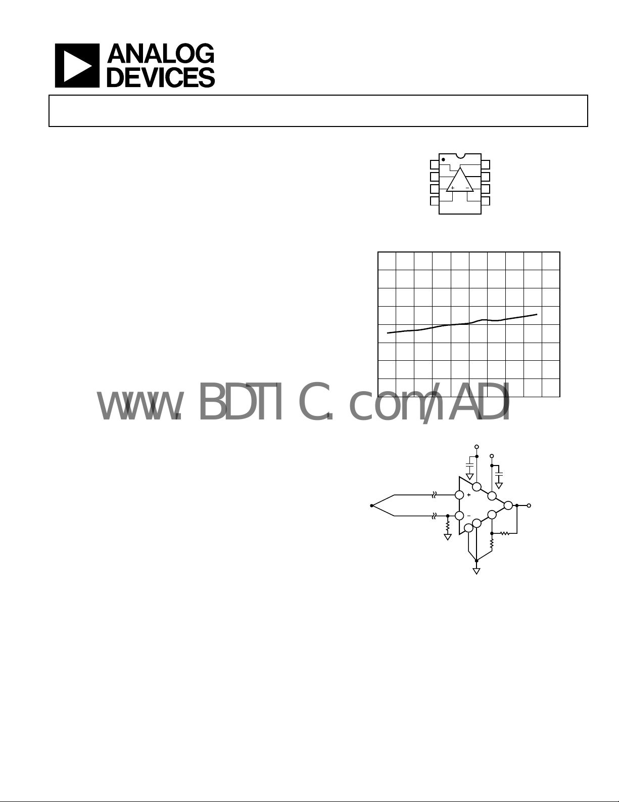
CONNECTION DIAGRAM
1
–V
S
2
+V
S
3
V
1
REF
4
+IN
AD8230
TOP VIEW
(Not to Scale)
Figure 1. 8-Lead SOIC (R-8)
2.0
1.5
1.0
0.5
0
–0.5
–1.0
OFFSET VOLTAGE (µV RTI)
–1.5
–2.0
TEMPERATURE ( °C)
Figure 2. Relative Offset Voltage vs. Temperature
0.1µF
TYPE K THERMO COUPLE
Figure 3. Thermocouple Measurement
The AD8230 is versatile yet simple to use. Its auto-zeroing
topology significantly minimizes the input and output
transients typical of commutating or chopper instrumentation
amplifiers. The AD8230 operates on ±4 V to ±8 V (+8 V to +16 V)
supplies and is available in an 8-lead SOIC.
1
The AD8230 can be programmed for a gain as low as 2, but the maximum
input voltage is limited to approximately 750 mV.
One Technology Way, P.O. Box 9106, Norwood, MA 02062-9106, U.S.A.
Tel: 781.329.4700 www.analog.com
Fax: 781.461.3113 ©2004–2007 Analog Devices, Inc. All rights reserved.
+5
4
AD8230
5
3
8
V
OUT
7
R
G
6
V
2
REF
5
–IN
05063-041
–5V
0.1µF
2
1
8
7
6
34.8kΩ
284Ω
05063-001
150–50 –30 –10 10 30 50 70 90 110 130
V
OUT
05063-002
Page 2

AD8230
www.BDTIC.com/ADI
TABLE OF CONTENTS
Features .............................................................................................. 1
Applications....................................................................................... 1
General Description......................................................................... 1
Connection Diagram .......................................................................1
Revision History ............................................................................... 2
Specifications..................................................................................... 3
Absolute Maximum Ratings............................................................ 5
Thermal Characteristics .............................................................. 5
ESD Caution.................................................................................. 5
Typical Performance Characteristics............................................. 6
Theory of Operation ...................................................................... 11
Setting the Gain .......................................................................... 11
REVISION HISTORY
9/07—Rev. A to Rev. B
Changes to Features and Layout..................................................... 1
Changes to Table 1............................................................................ 3
Changes to Table 2............................................................................ 4
Changes to Layout............................................................................ 5
Inserted Figure 13, Figure 14, and Figure 15; Renumbered
Sequentially ....................................................................................... 7
Changes to Figure 16 and Figure 19............................................... 8
Updated Outline Dimensions....................................................... 15
Level-Shifting the Output ......................................................... 12
Source Impedance and Input Settling Time........................... 12
Input Voltage Range................................................................... 13
Input Protection ......................................................................... 13
Power Supply Bypassing ............................................................ 13
Power Supply Bypassing for Multiple Channel Systems ....... 13
Layout .......................................................................................... 14
Applications ................................................................................ 14
Outline Dimensions ....................................................................... 15
Ordering Guide .......................................................................... 15
7/05—Rev. 0 to Rev. A
C
hanges to Excellent AC and DC Performance............................1
Changes to Table 1.............................................................................3
Changes to Table 2.............................................................................4
Changes to Figure 7 and Figure 8....................................................6
Changes to Figure 10 and Figure 11................................................7
Changes to Level-Shifting the Output Section........................... 11
Changes to Figure 31...................................................................... 11
Inserted Figure 32 and Figure 33; Renumbered Sequentially .. 11
Changes to Source Impedance and Input Settling Time Section,
Input Protection Section and Power Supply Bypassing for
Multiple Channel Systems Section............................................... 12
Changes to Figure 36...................................................................... 13
Changes to Applications Section.................................................. 13
10/04—Revision 0: Initial Version
Rev. B | Page 2 of 16
Page 3
AD8230
www.BDTIC.com/ADI
SPECIFICATIONS
VS = ±5 V, V
Table 1.
Parameter Conditions Min Typ Max Unit
VOLTAGE OFFSET
RTI Offset, V
Offset Drift
COMMON-MODE REJECTION (CMR)
CMR to 60 Hz with 1 kΩ Source Imbalance VCM = −5 V to +5 V 110 120 dB
VOLTAGE OFFSET RTI vs. SUPPLY (PSR)
G = 2 120 120 dB
G = 202 120 140 dB
GAIN G = 2(1 + RF/RG)
Gain Range 10
Gain Error
G = 2 0.01 0.04 %
G = 10 0.01 0.04 %
G = 100 0.01 0.04 %
G = 1000 0.02 0.05 %
Gain Nonlinearity 20 ppm
Gain Drift
G = 2, 10, 102 14 ppm/°C
G = 1002 60 ppm/°C
INPUT
Input Common-Mode Operating Voltage Range −V
Over Temperature T = −40°C to +125°C −V
Input Differential Operating Voltage Range 750 mV
Average Input Offset Current
Average Input Bias Current
OUTPUT
Output Swing −VS + 0.1 +VS − 0.2 V
Over Temperature T = −40°C to +125°C −VS + 0.1 +VS − 0.2 V
Short-Circuit Current 15 mA
REFERENCE INPUT
Voltage Range
NOISE
Voltage Noise Density, 1 kHz, RTI V
Voltage Noise f = 0.1 Hz to 10 Hz 3 μV p-p
SLEW RATE VIN = 500 mV, G = 10 2 V/μs
INTERNAL SAMPLE RATE 6 kHz
POWER SUPPLY
Operating Range (Dual Supplies) ±4 ±8 V
Operating Range (Single Supply) 8 16 V
Quiescent Current T = −40°C to +125°C 2.7 3.5 mA
TEMPERATURE RANGE
Specified Performance −40 +125 °C
1
The AD8230 can operate as low as G = 2. However, since the differential input range is limited to approximately 750 mV, the AD8230 configured at G < 10 does not
make use of the full output voltage range.
2
Gain drift is determined by the TC match of the external gain setting resistors.
3
Differential source resistance less than 10 kΩ does not result in voltage offset due to input bias current or mismatched series resistors.
4
For G < 10, the reference voltage range is limited to −VS + 4.24 V to +VS – 2.75 V.
= 0 V, RF = 100 kΩ, RG = 1 kΩ (@ TA = 25°C, G = 202, RL = 10 kΩ, unless otherwise noted).
REF
V
OSI
2
3
3
4
= V
+IN
V
+IN
T
A
= 0 V 10 μV
−IN
= V
= 0 V,
−IN
50 nV/°C
= −40°C to +125°C
1
S
S
VCM = 0 V 33 300 pA
VCM = 0 V 0.15 1 nA
−VS + 3.5 +VS − 2.5 V
, V
, V
IN+
= 0 V 240 nV/√Hz
IN−
REF
1000 V/V
+V
+V
S
S
V
V
Rev. B | Page 3 of 16
Page 4
AD8230
www.BDTIC.com/ADI
VS = ±8 V, V
Table 2.
Parameter Conditions Min Typ Max Unit
VOLTAGE OFFSET
RTI Offset, V
Offset Drift
COMMON-MODE REJECTION (CMR)
CMR to 60 Hz with 1 kΩ Source Imbalance VCM = −8 V to +8 V 110 120 dB
VOLTAGE OFFSET RTI vs. SUPPLY (PSR)
G = 2 120 120 dB
G = 202 120 140 dB
GAIN G = 2(1 + RF/RG)
Gain Range 10
Gain Error
G = 2 0.01 0.04 %
G = 10 0.01 0.04 %
G = 100 0.01 0.04 %
G = 1000 0.02 0.05 %
Gain Nonlinearity 20 ppm
Gain Drift
G = 2, 10, 102 14 ppm/°C
G=1002 60 ppm/°C
INPUT
Input Common-Mode Operating Voltage Range −V
Over Temperature T = −40°C to +125°C −V
Input Differential Operating Voltage Range 750 mV
Average Input Offset Current
Average Input Bias Current
OUTPUT
Output Swing −VS + 0.1 +VS − 0.2 V
Over Temperature T = −40°C to +125°C −VS + 0.1 +VS − 0.4 V
Short-Circuit Current 15 mA
REFERENCE INPUT
Voltage Range
NOISE
Voltage Noise Density, 1 kHz, RTI V
Voltage Noise f = 0.1 Hz to 10 Hz 3 μV p-p
SLEW RATE VIN = 500 mV, G = 10 2 V/μs
INTERNAL SAMPLE RATE 6 kHz
POWER SUPPLY
Operating Range (Dual Supplies) ±4 ±8 V
Operating Range (Single Supply) 8 16 V
Quiescent Current T = −40°C to +125°C 3.2 4 mA
TEMPERATURE RANGE
Specified Performance −40 +125 °C
1
The AD8230 can operate as low as G = 2. However, since the differential input range is limited to approximately 750 mV, the AD8230 configured at G < 10 does not
make use of the full output voltage range.
2
Gain drift is determined by the TC match of the external gain setting resistors.
3
Differential source resistance less than 10 kΩ does not result in voltage offset due to input bias current or mismatched series resistors.
4
For G < 10, the reference voltage range is limited to −VS + 4.24 V to +VS − 2.75V.
= 0 V, RF = 100 kΩ, RG = 1 kΩ (@ TA = 25°C, G = 202, RL = 10 kΩ, unless otherwise noted).
REF
V
OSI
= V
+IN
V
+IN
= 0 V 20 μV
−IN
= V
= 0 V,
−IN
50 nV/°C
T = −40°C to +125°C
1
2
3
3
4
S
S
VCM = 0 V 33 300 pA
VCM = 0 V 0.15 1 nA
−VS + 3.5 +VS − 2.5 V
, V
, V
IN+
= 0 V 240 nV/√Hz
IN−
REF
1000 V/V
+V
+V
S
S
V
V
Rev. B | Page 4 of 16
Page 5

AD8230
www.BDTIC.com/ADI
ABSOLUTE MAXIMUM RATINGS
Table 3.
Parameter Rating
Supply Voltage ±8 V, +16 V
Internal Power Dissipation 304 mW
Output Short-Circuit Current 20 mA
Input Voltage (Common-Mode) ±V
Differential Input Voltage ±V
Storage Temperature Range −65°C to +150°C
Operational Temperature Range −40°C to +125°C
Stresses above those listed under Absolute Maximum Ratings
may cause permanent damage to the device. This is a stress
rating only; functional operation of the device at these or any
other conditions above those indicated in the operational
section of this specification is not implied. Exposure to absolute
maximum rating conditions for extended periods may affect
device reliability.
S
S
THERMAL CHARACTERISTICS
Specification is for device in free air SOIC.
Table 4.
Parameter Value Unit
θJA (4-Layer JEDEC Board) 121 °C/W
ESD CAUTION
Rev. B | Page 5 of 16
Page 6

AD8230
www.BDTIC.com/ADI
TYPICAL PERFORMANCE CHARACTERISTICS
20
NORMALIZ ED FOR VCM = 0V
15
500
TOTAL NUMBER OF
SAMPLES = 2839 FROM 3 L OTS
400
300
SAMPLES
200
100
0
OFFSET VOLTAGE (µV RTI)
Figure 4. Offset Voltage (RTI) Distribution at ±5 V, CM = 0 V, T
40
35
30
25
20
SAMPLES
15
10
5
0
TOTAL NUMBER OF SAMPLES = 300 FROM 3 LOTS
OFFSET VOLTAGE DRIFT (nV/°C)
Figure 5. Offset Voltage (RTI) Drift Distribution
0
–2
–4
–6
–8
–10
–12
–14
OFFSET VOLTAGE (µV RTI)
–16
–18
–20
TEMPERATURE ( °C)
VS =±5V
=±8V
V
S
Figure 6. Offset Voltage (RTI) vs. Temperature
9–9 –3–6 0 3 6
= 25°C
A
50–50 –30 –10 10 30
150–50 –30 –10 10 7030 50 110 13090
10
5
0
–5
–10
OFFSET VOLTAGE (µV RTI)
–15
05063-004
–20
–2 0–6 –4 2 4 6
COMMON-MODE VOLTAGE (V)
Figure 7. Offset Voltage (RTI) vs. Common-Mode Voltage, V
= ±5 V
S
05063-007
20
NORMALIZ ED FOR VCM = 0V
15
10
5
0
–5
–10
OFFSET VOLTAGE (µV RTI)
–15
05063-005
–20
–10–8–6–4–2 0 2 4 6 8 10
COMMON-MODE VOLTAGE (V)
Figure 8. Offset Voltage (RTI) vs. Common-Mode Voltage, V
= ±8 V
S
05063-008
0
–1
–2
–3
–4
–5
OFFSET VOLTAGE (µV)
–6
–7
05063-006
–8
Figure 9. Offset Voltage (RTI) vs. Source
±5V SUPPLY
±8V SUPPLY
2301 45
SOURCE IMPEDANCE (kΩ)
Impedance, 1 μF Across Input Pins
05063-009
6
Rev. B | Page 6 of 16
Page 7

AD8230
www.BDTIC.com/ADI
40
NORMALIZ ED FOR V
30
20
10
0
–10
–20
OFFSET VOLTAGE (µV RTI)
–30
–40
= 0V
REF
–0.5 0–1.5 –1.0 0.5 1.0 1.5
V
(V)
REF
Figure 10. Offset Voltage (RTI) vs. Reference Voltage
130
120
110
100
90
80
CMR (dB)
70
60
50
40
10 100 1k 10k
CMR WITH NO SOURCE IMBAL ANCE
CMR WITH 1kΩ SO URCE IMBALANCE
FREQUENCY (Hz)
Figure 11. Common-Mode Rejection (CMR) vs. Frequency
130
128
126
124
122
120
CMR (dB)
118
116
114
112
110
±5V SUPPLY
±8V SUPPLY
4602 81012
SOURCE IMPEDANCE (kΩ)
Figure 12. Common-Mode Rejection (CMR) vs.
Sour
ce Impedance, 1.1 μF Across Input Pins
05063-010
05063-011
05063-012
10
–856mV, +8.2V 0V, +8.4V +592mV, +8.2V
8
6
–812mV, +5V
4
2
0
–2
–4
–6
–8
INPUT COMMON-MODE VO LTAGE RANGE (V)
–616mV, –8.2V
–10
–800 –600 –400 –200 0 200 400 600 800
–1000 1000
VS = ±8V
–652mV, –5V
OUTPUT VOLTAGE (mV)
0V, +5.5V
VS = ±5V
0V, –5.5V
0V, –8.4V
+644mV, +5V
+800mV, –5V
+840mV, –8.2V
05063-013
Figure 13. Input Common-Mode Voltage Range vs. Output Voltage, G = 2
10
–7.9V, +8V
8
–4.9V, +5V
6
4
2
0
–2
–4
–6
–8
INPUT COMMO N-MODE VOL TAGE RANGE (V)
–7.9V, –8V +7.9V, –8V
–10
–10 10
–8 –6 –4 –2 0 2 4 6 8
VS = ±8V
VS = ±5V
OUTPUT VOLTAGE (V)
+7.9V, +8V
+4.88V, +5V
+4.88V, –5V–4.9V, –5V
05063-014
Figure 14. Input Common-Mode Voltage Range vs. Output Voltage, G = 10
10
8
6
4
2
0
–2
–4
–6
–8
INPUT COMMO N-MODE VOL TAGE RANGE (V)
–7.9V, –8V + 7.9V, –8V
–10
–10 10
–8 –6 –4 –2 0 2 4 6 8
VS = ±8V
–4.8V, +5. 5V +4.8V, +5.5V
VS = ±5V
–4.8V, –5.5V +4.8V, –5. 5V
OUTPUT VOLTAGE (V)
+7.9V, +8V–7.9V, +8V
05063-015
Figure 15. Input Common-Mode Voltage Range vs. Output Voltage, G = 100
Rev. B | Page 7 of 16
Page 8

AD8230
www.BDTIC.com/ADI
6.8
6.6
6.4
±8V
6.2
6.0
5.8
CLOCK FREQUENCY (kHz)
5.6
5.4
–50 –30 –10 10 30 50 70 90 110 1 30
TEMPERATURE ( °C)
Figure 16. Clock Frequen
±5V
cy vs. Temperature
1.0
0.8
0.6
0.4
0.2
0
–0.2
–0.4
0°C
–0.6
AVERAGE INPUT BIAS CURRENT (µA)
–0.8
–1.0
+25°C
–2 0–6 –4 2 4 6
COMMON-MODE VOLTAGE (V)
+85°C
+125°C
Figure 17. Average Input Bias Current vs. Common-Mode Voltage,
−4
0°C, +25°C, +85°C, +125°C
3.5
3.4
3.3
3.2
3.1
3.0
2.9
2.8
SUPPLY CURRENT (mA)
2.7
2.6
2.5
0–50 50 100 150
TEMPERATURE ( °C)
±8V
±5V
Figure 18. Supply Current vs. Temperature
–40°C
90
80
70
60
50
40
GAIN (dB)
30
20
10
0
05063-016
–10
10010 1k 10k 100k
FREQUENCY (Hz)
05063-019
Figure 19. Gain vs. Frequency, G = 2
90
80
70
60
50
40
GAIN (dB)
30
20
10
0
05063-017
–10
10010 1k 10k 100k
FREQUENCY (Hz)
05063-020
Figure 20. Gain vs. Frequency, G = 10
40
G = +20
30
20
10
0
–10
NONLINEARIT Y (ppm)
–20
–30
05063-018
–40
–5 –4 –3 –2 –1 0 1 2 3 4 5
V
(V)
OUT
05063-021
Figure 21. Gain Nonlinearity, G = 20
Rev. B | Page 8 of 16
Page 9

AD8230
www.BDTIC.com/ADI
90
80
70
60
50
40
GAIN (dB)
30
20
10
0
–10
10010 1k 10k 100k
FREQUENCY (Hz)
Figure 22. Gain vs. Frequency, G = 100
90
80
70
60
50
40
GAIN (dB)
30
20
10
0
–10
10010 1k 10k 100k
FREQUENCY (Hz)
Figure 23. Gain vs. Frequency, G = 1000
0.010
0.008
0.006
0.004
0.002
0
–0.002
GAIN ERROR (%)
–0.004
–0.006
–0.008
–0.010
501015
SOURCE IMPEDANCE (kΩ)
Figure 24. Gain Error vs. Differential Source Impedance
05063-022
05063-023
05063-024
20
0.35
0.30
0.25
0.20
0.15
0.10
VOLTAGE NOISE (µV/ Hz)
0.05
0
FREQUENCY (Hz)
Figure 25. Voltage Noise Spectral Density vs. Frequency
3.90
3.70
3.50
3.30
3.10
2.90
POSITI VE SUPPLY CURRENT (mA)
2.70
2.50
2µV/DIV 1s/DIV
–50 –30 –10 10 30 50 70 90 110 130
TEMPERATURE (°C)
Figure 26. 0.1 Hz to 10 Hz RTI Voltage Noise, G = 100
160
140
G = +100
G = +2
G = +1000
G = +10
120
100
80
PSR (dB)
60
40
20
0
0.1 1 10
FREQUENCY (kHz)
Figure 27. Positive PSR vs. Frequency, RTI
05063-025
100k1 10 100 1k 10k
05063-026
05063-027
Rev. B | Page 9 of 16
Page 10

AD8230
www.BDTIC.com/ADI
140
120
100
80
60
PSR (dB)
40
20
0
0.1 1 10
G = +100
G = +1000
G = +2
FREQUENCY (kHz)
G = +10
05063-028
Figure 28. Negative PSR vs. Frequency, RTI
10
V
=±8V
S
8
6
4
VS =±5V
2
0
–2
=±5V
V
S
–4
–6
OUTPUT VOLTAGE SWING (V)
–8
V
=±8V
S
–10
–40°C
+125°C
+125°C
°
–40
OUTPUT CURRENT (mA)
–40°C
C
+125
Figure 29. Output Voltage Swing vs. Output Current,
−4
0°C, +25°C, +85°C, +125°C
+125°C
+25°C
+25°C
+25°C
°
C
–40
+25°C
°
C
05063-029
120246810
Rev. B | Page 10 of 16
Page 11

AD8230
T
V
+V
T
V
+V
V
www.BDTIC.com/ADI
THEORY OF OPERATION
Auto-zeroing is a dynamic offset and drift cancellation
technique that reduces input-referred voltage offset to the
μV level and voltage offset drift to the nV/°C level. A further
advantage of dynamic offset cancellation is the reduction of
low frequency noise, in particular the 1/f component.
The AD8230 is an instrumentation amplifier that uses an
a
uto-zeroing topology and combines it with high commonmode signal rejection. The internal signal path consists of an
active differential sample-and-hold stage (preamp) followed by
a differential amplifier (gain amp). Both amplifiers implement
auto-zeroing to minimize offset and drift. A fully differential
topology increases the immunity of the signals to parasitic noise
and temperature effects. Amplifier gain is set by two external
resistors for convenient TC matching.
The signal sampling rate is controlled by an on-chip, 6 kHz
o
scillator and logic to derive the required nonoverlapping
clock phases. For simplification of the functional description,
two sequential clock phases, A and B, are shown to distinguish
the order of internal operation, as depicted in
Figure 30 and
Figure 31, respectively.
–V
–V
S
S
R
G
GAIN AMP
C
HOLD
C
HOLD
V
OU
R
F
05063-030
PREAMP
V
DIFF
+IN
C
CM
V
–IN
SAMPLE
–
+
–
+
V
REF
Figure 30. Phase A of the Sampling Phase
During Phase A, the sampling capacitors are connected to the
inputs. The input signal’s difference voltage, V
across the sampling capacitors, C
. Because the sampling
SAMPLE
, is stored
DIFF
capacitors only retain the difference voltage, the common-mode
voltage is rejected. During this period, the gain amplifier is not
connected to the preamplifier so its output remains at the level
set by the previously sampled input signal held on C
HOLD
, as
shown in Figure 30.
–V
–V
S
S
R
C
HOLD
C
HOLD
G
GAIN AMP
V
OU
R
F
05063-031
PREAMP
V
DIFF
+IN
C
CM
V
–IN
SAMPLE
–
+
–
+
V
REF
Figure 31. Phase B of the Sampling Phase
In Phase B, the differential signal is transferred to the hold
capacitors refreshing the value stored on C
. The output of
HOLD
the preamplifier is held at a common-mode voltage determined
by the reference potential, V
. In this manner, the AD8230 is
REF
able to condition the difference signal and set the output voltage
level. The gain amplifier conditions the updated signal stored
on the hold capacitors, C
HOLD
.
SETTING THE GAIN
Two external resistors set the gain of the AD8230. The gain is
expressed in the following equation:
R
10µF
F
F
)2(1
(1)
R
G
+
S
–V
S
0.1µF
4
AD8230
5
V
REF
3
0.1µF
2
1
R
G
2
V
7
REF
6
1
R
F
R
G
10µF
V
8
OUT
05063-032
Figure 32. Gain Setting
R
G
Actual Gain
50.5
99.6
202
501
, small. This is due
F
pin, Pin 7. The effect
G
Gain +=
Table 5. Gains Using Standard 1% Resistors
Gain R
2 0 Ω (short) None 2
10 8.06 kΩ 2 kΩ 10
50 12.1 kΩ 499 Ω
100 9.76 kΩ 200 Ω
200 10 kΩ 100 Ω
500 49.9 kΩ 200 Ω
1000 100 kΩ 200 Ω 1002
Figure 32 and Tab l e 5 provide an example of some gain settings.
As Ta ble 5 shows, the AD8230 accepts a wide range of resistor
va
lues. Because the instrumentation amplifier has finite driving
capability, ensure that the output load in parallel with the sum
of the gain setting resistors is greater than 2 kΩ.
R
||(RF + RG) > 2 kΩ (2)
L
Offset voltage drift at high temperature can be minimized by
eeping the value of the feedback resistor, R
k
to the junction leakage current on the R
of the gain setting resistor on offset voltage drift is shown in
Figure 33. In addition, experience has shown that wire-wound
esistors in the gain feedback loop may degrade the offset
r
voltage performance.
Rev. B | Page 11 of 16
Page 12

AD8230
V
×
V
V
www.BDTIC.com/ADI
0
–1
–2
–3
OFFSET VOLTAGE (µV RTI)
–4
–5
TEMPERATURE (°C)
Figure 33. Effect of Feedback Resi
RF = 100kΩ, RG = 1kΩ
= 10kΩ, RG = 100Ω
R
F
stor on Offset Voltage Drift
05063-033
150–50 0 50 100
LEVEL-SHIFTING THE OUTPUT
A reference voltage, as shown in Figure 34, can be used to
level-shift the output. The reference voltage, V
+ 3.5 V to +VS − 2.5 V. (For G < 10, the reference voltage
−V
S
range is limited to −V
+ 4.24 V to +VS – 2.75 V.) Otherwise, it
S
is nominally tied to midsupply. The voltage source used to levelshift the output should have a low output impedance to avoid
contributing to gain error. In addition, it should be able to
source and sink current. To minimize offset voltage, the V
pins should be connected either to the local ground or to a
reference voltage source that is connected to the local ground.
+
S
–V
S
0.1µF
0.1µF
2
4
5
AD8230
6
3
1
8
7
R
F
R
G
V
R
Figure 34. Level-Shifting the Output
The output can also be level-shifted by adding a resistor, RO, as
shown in Figure 35. The benefit is that the output can be level-
hifted to as low as 100 mV of the negative supply rail and to as
s
high as 200 mV of the positive supply rail, increasing unipolar
output swing. This can be useful in applications, such as strain
gauges, where the force is only applied in one direction. Another
benefit of this configuration is that a supply rail can be used for
eliminating the need to add an additional external reference
V
R’
voltage.
The gain changes with the inclusion of R
⎛
⎜
V −
2
OUT
⎜
⎝
⎞
R
F
+= 121
RR
||
OG
R
⎟
V
IN
⎟
R
⎠
⎛
()
F
V
O
F
⎜
=−
R'
⎜
RR
⎝
, is limited to
R
REF
V
OUT
05063-034
. The full expression is
O
⎞
RRR
+
OG
+
OG
R
F
⎟
⎟
⎠
V
V
IN
R
'
R
O
(3)
The following steps can be taken to set the gain and level-shift
e output:
th
1.
Select an R
Solve for R
2.
R
value. Table 5 shows RF values for various gains.
F
using Equation 4.
O
RV
F
R'
−= (4)
O
V
DESIRED
LEVEL
−
where:
is a voltage source, such as a supply voltage.
V
R’
V
DESIRED-LEVEL
Solve for R
3.
is the desired output bias voltage.
.
G
R
Gain
O
⎞
−
⎟
⎠
0.1µF
(5)
R
O
112−
R
F
+
S
–V
2
4
AD8230
5
6
3
=
R
G
⎛
⎜
⎝
S
0.1µF
1
7
R
G
V
8
VR'
OUT
R
F
R
O
5063-035
Figure 35. Level-Shifting the Output Without an
A
dditional Voltage Reference
+5
–5V
0.1µF
4
AD8230
5
3
0.1µF
2
1
7
6
203Ω
V
8
+5V
9.76kΩ
10.2kΩ
OUT
5063-036
Figure 36. An AD8230 with its Output Biased at −4.8 V;
G =
100; V
DESIRED-LEVEL
= −4.8 V
SOURCE IMPEDANCE AND INPUT SETTLING TIME
The input stage of the AD8230 consists of two actively driven,
differential switched capacitors, as described in Figure 30 and
Figure 31. Differential input signals are sampled on C
that the associated parasitic capacitances, 70 pF, are balanced
between the inputs to achieve high common-mode rejection.
On each sample period (approximately 85 μs), these parasitic
capacitances must be recharged to the common-mode voltage
by the signal source impedance (10 kΩ maximum). If resistors
and capacitors are used at the input of the AD8230, care should
be taken to maintain close match to maximize CMRR.
SAMPLE
such
Rev. B | Page 12 of 16
Page 13

AD8230
V
–V
www.BDTIC.com/ADI
INPUT VOLTAGE RANGE
The input common-mode range of the AD8230 is rail to rail.
However, the differential input voltage range is limited to
approximately 750 mV. The AD8230 does not phase invert
when its inputs are overdriven.
INPUT PROTECTION
The input voltage is limited to within 0.6 V beyond the supply
rails by the internal ESD protection diodes. Resistors and low
leakage diodes can be used to limit excessive, external voltage
and current from damaging the inputs, as shown in Figure 37.
Figure 39 shows an overvoltage protection circuit between the
th
ermocouple and the AD8230.
+
S
–V
BAV199
0.1µF
+V
–V
S
S
2.49kΩ
2.49kΩ
+V
BAV199
4
AD8230
5
–V
S
S
Figure 37. Overvoltage Input Protection
S
+V
S
10µF
10µF
0.1µF
0.1µF
1
2
3
4
–V
S
+V
S
AD8230
S
0.1µF
2
1
7
6
19.1kΩ
3
200Ω
8
7
6
5
8
0.1µF
V
OUT
05063-037
1µF 1µF 1µF
0.1µF
–V
S
1
+V
S
2
3
4
AD8230
8
7
6
0.1µF
5
POWER SUPPLY BYPASSING
A regulated dc voltage should be used to power the
instrumentation amplifier. Noise on the supply pins can
adversely affect performance. Bypass capacitors should be
used to decouple the amplifier.
The AD8230 has internal clocked circuitry that requires
quate supply bypassing. A 0.1 μF capacitor should be placed
ade
as close to each supply pin as possible. As shown in Figure 32, a
10 μ
F tantalum capacitor can be used further away from the part.
POWER SUPPLY BYPASSING FOR MULTIPLE CHANNEL SYSTEMS
The best way to prevent clock interference in multichannel
systems is to lay out the PCB with a star node for the positive
supply and a star node for the negative supply. Using such a
technique, crosstalk between clocks is minimized. If laying out
star nodes is not feasible, use wide traces to minimize parasitic
inductance and decouple frequently along the power supply
traces. Examples are shown in Figure 38. Care and forethought
a long way in maximizing performance.
go
1µF
0.1µF
1
2
3
4
–V
S
+V
S
AD8230
0.1µF
–V
S
0.1µF
1
+V
2
3
4
S
AD8230
8
7
6
5
0.1µF
–V
S
0.1µF
1
+V
2
3
4
S
AD8230
8
7
6
5
8
7
6
5
STAR –V
S
10µF
STAR +V
S
10µF
0.1µF
0.1µF
–V
1
+V
2
3
4
S
S
AD8230
0.1µF
0.1µF
–V
S
1
+V
2
3
4
S
AD8230
8
7
6
0.1µF
5
Figure 38. Use Star Nodes for +V
0.1µF
1
+V
2
3
4
–V
S
S
AD8230
8
7
6
5
and −VS or Use Thick Traces and Decouple Frequently Along the Supply Lines
S
Rev. B | Page 13 of 16
0.1µF
–V
S
1
8
7
6
5
0.1µF
+V
2
3
4
S
AD8230
8
7
6
5
05063-038
Page 14

AD8230
V
V
www.BDTIC.com/ADI
LAYOUT
The AD8230 has two reference pins: V
draws current to set the internal voltage references. In contrast,
V
2 does not draw current. It sets the common mode of the
REF
output signal. As such, V
1 and V
REF
ground (or to a reference voltage). In addition, to maximize
CMR, the trace between V
2 and the gain resistor, RG, should
REF
be kept short.
1 and V
REF
2 should be star-connected to
REF
REF
2. V
REF
1
APPLICATIONS
The AD8230 can be used in thermocouple applications, as
shown in Figure 3 and Figure 39. Figure 39 is an example of
s
uch a circuit for use in an industrial environment. Series
resistors and low leakage diodes serve to clamp overload
voltages (see the
THERMOCOUPL E
Figure 39. Type J Thermocouple with Overvoltage Protection and RFI Filter
Input Protection section for more information).
+
–V
0.1µF
–V
S
S
4
AD8230
5
3
S
–V
S
0.1µF
2
1
8
7
6
19.1kΩ
200Ω
TYPE J
100MΩ
100MΩ
+V
4.99kΩ
4.99kΩ
–V
BAV199
+V
S
S
1µF
S
+V
S
BAV199
V
OUT
5063-039
An antialiasing filter reduces unwanted high frequency signals.
The matched 100 MΩ resistors serve to provide input bias
current to the input transistors and serve as an indicator as to
when the thermocouple connection is broken. Well-matched
1% 4.99 kΩ resistors are used to form the antialiasing filter. It is
good practice to match the source impedances to ensure high
CMR. The circuit is configured for a gain of 193, which
provides an overall temperature sensitivity of 10 mV/°C.
+
S
–V
S
0.1µF
+V
S
350Ω 350Ω
350Ω 350Ω
–V
S
4
AD8230
5
3
0.1µF
2
1
7
6
102kΩ
1kΩ
4kΩ
8
1µF
V
OUT
05063-040
Figure 40. Bridge Measurement with Filtered Output
Measuring load cells in industrial environments can be a
challenge. Often, the load cell is located some distance away
from the instrumentation amplifier. The common-mode
potential can be several volts, exceeding the common-mode
input range of many 5 V auto-zero instrumentation amplifiers.
Fortunately, the wide common-mode input voltage range of the
AD8230 spans 16 V, relieving designers of having to worry
about the common-mode range.
Rev. B | Page 14 of 16
Page 15

AD8230
www.BDTIC.com/ADI
OUTLINE DIMENSIONS
5.00 (0.1968)
4.80 (0.1890)
4.00 (0.1574)
3.80 (0.1497)
0.25 (0.0098)
0.10 (0.0040)
COPLANARITY
0.10
CONTROLL ING DIMENSI ONS ARE IN MILLIMETERS; INCH DI MENSIONS
(IN PARENTHESES) ARE ROUNDED-OFF MILLIMETER EQUIVALENTS FOR
REFERENCE ONLY AND ARE NOT APPROPRI ATE FOR USE IN DES IGN.
85
1
1.27 (0.0500)
SEATING
PLANE
COMPLIANT TO JEDEC STANDARDS MS-012-A A
BSC
6.20 (0.2441)
5.80 (0.2284)
4
1.75 (0.0688)
1.35 (0.0532)
0.51 (0.0201)
0.31 (0.0122)
8°
0°
0.25 (0.0098)
0.17 (0.0067)
0.50 (0.0196)
0.25 (0.0099)
1.27 (0.0500)
0.40 (0.0157)
45°
012407-A
Figure 41. 8-Lead Standard Small Outline Package [SOIC_N]
Narrow B
ody (R-8)
Dimensions shown in millimeters and (inches)
ORDERING GUIDE
Model Temperature Range Package Description Package Option
AD8230YRZ
AD8230YRZ-REEL
AD8230YRZ-REEL7
AD8230-EVAL Evaluation Boar
1
Z = RoHS Compliant Part.
1
1
1
−40°C to +125°C 8-Lead SOIC_N R-8
−40°C to +125°C 8-Lead SOIC_N, 13" Tape and Reel R-8
−40°C to +125°C 8-Lead SOIC_N, 7" Tape and Reel R-8
d
Rev. B | Page 15 of 16
Page 16

AD8230
www.BDTIC.com/ADI
NOTES
©2004–2007 Analog Devices, Inc. All rights reserved. Trademarks and
registered trademarks are the property of their respective owners.
D05063-0-9/07(B)
Rev. B | Page 16 of 16
 Loading...