

Page 1
Dual, 16 MHz, Rail-to-Rail
1
2
3
4
8
7
6
5
AD823
OUT1
+IN2
–IN2
OUT2
+V
S
–IN1
+IN1
–V
S
FREQUENCY – Hz
–8
OUTPUT – dB
1k
–6
–7
2
1
10k 100k 1M
VS = +5V
G = +1
–5
–4
–3
–2
–1
0
10M
a
FEATURES
Single Supply Operation
Output Swings Rail to Rail
Input Voltage Range Extends Below Ground
Single Supply Capability from +3 V to +36 V
High Load Drive
Capacitive Load Drive of 500 pF, G = +1
Output Current of 15 mA, 0.5 V from Supplies
Excellent AC Performance on 2.6 mA/Amplifier
–3 dB Bandwidth of 16 MHz, G = +1
350 ns Settling Time to 0.01% (2 V Step)
Slew Rate of 22 V/ms
Good DC Performance
800 mV Max Input Offset Voltage
2 mV/8C Offset Voltage Drift
25 pA Max Input Bias Current
Low Distortion
–108 dBc Worst Harmonic @ 20 kHz
Low Noise
16 nV/√
No Phase Inversion with Inputs to the Supply Rails
Hz @ 10 kHz
FET Input Amplifier
AD823
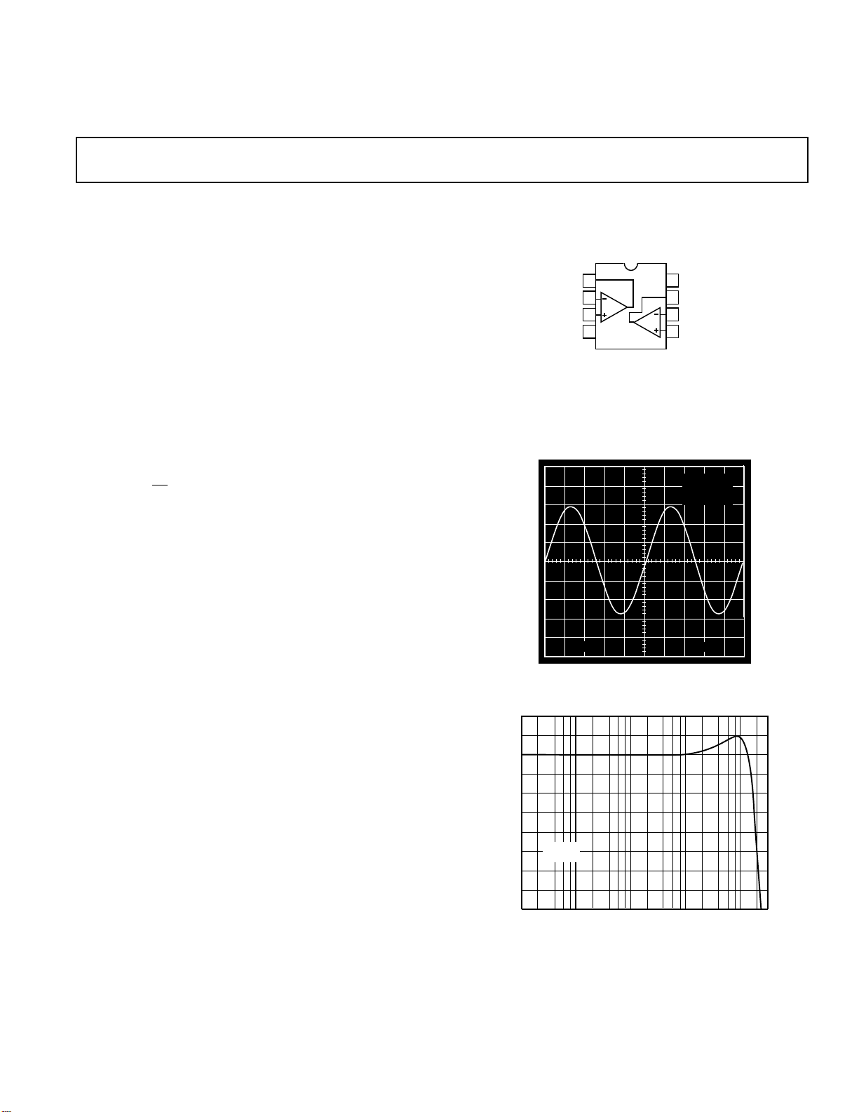
CONNECTION DIAGRAM
8-Pin Plastic Mini-DIP
and
8-Lead SOIC
The AD823 is available over the industrial temperature range of
–40°C to +85°C and is offered in both 8-pin plastic DIP and
SOIC packages.
RL = 100kΩ
= 50pF
C
L
V
= +3V
3V
S
APPLICATIONS
Battery Powered Precision Instrumentation
Photodiode Preamps
Active Filters
12- to 16-Bit Data Acquisition Systems
Medical Instrumentation
PRODUCT DESCRIPTION
The AD823 is a dual precision, 16 MHz, JFET input op amp
that can operate from a single supply of +3.0 V to +36 V, or
dual supplies of ±1.5 V to ±18 V. It has true single supply
capability with an input voltage range extending below ground
in single supply mode. Output voltage swing extends to within
50 mV of each rail for I
≤ 100 µA providing outstanding out-
OUT
put dynamic range.
Offset voltage of 800 µV max, offset voltage drift of 2 µV/°C,
input bias currents below 25 pA and low input voltage noise
provide dc precision with source impedances up to a Gigohm.
16 MHz, –3 dB bandwidth, –108 dB THD @ 20 kHz and
22 V/µs slew rate are provided with a low supply current of
2.6 mA per amplifier. The AD823 drives up to 500 pF of direct
capacitive load as a follower, and provides an output current of
15 mA, 0.5 V from the supply rails. This allows the amplifier to
handle a wide range of load conditions.
This combination of ac and dc performance, plus the outstanding load drive capability results in an exceptionally versatile amplifier for applications such as A/D drivers, high-speed active
filters, and other low voltage, high dynamic range systems.
REV. 0
Information furnished by Analog Devices is believed to be accurate and
reliable. However, no responsibility is assumed by Analog Devices for its
use, nor for any infringements of patents or other rights of third parties
which may result from its use. No license is granted by implication or
otherwise under any patent or patent rights of Analog Devices.
GND
500mV
200µs
Figure 1. Output Swing, VS = +3 V, G = +1
Figure 2. Small Signal Bandwidth, G = +1
© Analog Devices, Inc., 1995
One Technology Way, P.O. Box 9106, Norwood. MA 02062-9106, U.S.A.
Tel: 617/329-4700 Fax: 617/326-8703
Page 2

AD823–SPECIFICATIONS
(@ TA = +25°C, VS = +5 V, RL = 2 kΩ to +2.5 V, unless otherwise noted)
AD823A
Parameter Conditions Min Typ Max Units
DYNAMIC PERFORMANCE
–3 dB Bandwidth, V
Full Power Response V
Slew Rate G = –1, V
Settling Time G = –1, V
≤ 0.2 V p-p G = +1 12 16 MHz
O
= 2 V p-p 3.5 MHz
O
= 4 V Step 14 22 V/µs
O
= 2 V Step
O
to 0.1% 320 ns
to 0.01% 350 ns
NOISE/DISTORTION PERFORMANCE
Input Voltage Noise f = 10 kHz 16 nV/√
Input Current Noise f = 1 kHz 1 fA/√
Harmonic Distortion R
= 600 Ω to 2.5 V, V
L
= 2 V p-p, –108 dBc
O
Hz
Hz
f = 20 kHz
Crosstalk
f = 1 kHz R
f = 1 MHz R
= 5 kΩ –130 dB
L
= 5 kΩ –93 dB
L
DC PERFORMANCE
Initial Offset 0.2 0.8 mV
Max Offset Over Temperature 0.3 2.0 mV
Offset Drift 2 µV/°C
Input Bias Current V
at T
MAX
= 0 V to +4 V 3 25 pA
CM
0.5 5 nA
Input Offset Current 220pA
at T
MAX
Open-Loop Gain V
T
to T
MIN
MAX
= 0.2 V to 4 V
O
R
= 2 kΩ 20 45 V/mV
L
20 V/mV
0.5 nA
INPUT CHARACTERISTICS
Input Common-Mode Voltage Range –0.2 to 3 –0.2 to 3.8 V
Input Resistance 10
13
Ω
Input Capacitance 1.8 pF
Common-Mode Rejection Ratio VCM = 0 V to 3 V 60 76 dB
OUTPUT CHARACTERISTICS
Output Voltage Swing
I
= ±100 µA 0.025 to 4.975 V
L
I
= ±2 mA 0.08 to 4.92 V
L
I
= ±10 mA 0.25 to 4.75 V
L
Output Current V
= 0.5 V to 4.5 V 16 mA
OUT
Short Circuit Current Sourcing to 2.5 V 40 mA
Sinking to 2.5 V 30 mA
Capacitive Load Drive G = +1 500 pF
POWER SUPPLY
Operating Range +3 +36 V
Quiescent Current T
Power Supply Rejection Ratio VS = +5 V to +15 V, T
Specification subject to change without notice.
MIN
to T
, Total 5.2 5.6 mA
MAX
MIN
to T
MAX
70 80 dB
–2–
REV. 0
Page 3

AD823
SPECIFICATIONS
(@ TA = +25°C, VS = +3.3 V, RL = 2 kΩ to +1.65 V, unless otherwise noted)
AD823A
Parameter Conditions Min Typ Max Units
DYNAMIC PERFORMANCE
–3 dB Bandwidth, V
Full Power Response V
Slew Rate G = –1, V
Settling Time G = –1, V
≤ 0.2 V p-p G = +1 12 15 MHz
O
= 2 V p-p 3.2 MHz
O
= 2 V Step 13 20 V/µs
O
= 2 V Step
O
to 0.1% 250 ns
to 0.01% 300 ns
NOISE/DISTORTION PERFORMANCE
Input Voltage Noise f = 10 kHz 16 nV/√
Input Current Noise f = 1 kHz 1 fA/√
Harmonic Distortion R
= 100 Ω, V
L
= 2 V p-p, f = 20 kHz –93 dBc
O
Hz
Hz
Crosstalk
f = 1 kHz R
f = 1 MHz R
= 5 kΩ –130 dB
L
= 5 kΩ –93 dB
L
DC PERFORMANCE
Initial Offset 0.2 1.5 mV
Max Offset Over Temperature 0.5 2.5 mV
Offset Drift 2 µV/°C
Input Bias Current V
at T
MAX
= 0 V to +2 V 3 25 pA
CM
0.5 5 nA
Input Offset Current 220pA
at T
MAX
Open-Loop Gain V
T
to T
MIN
MAX
= 0.2 V to 2 V
O
R
= 2 kΩ 15 30 V/mV
L
12 V/mV
0.5 nA
INPUT CHARACTERISTICS
Input Common-Mode Voltage Range –0.2 to 1 –0.2 to 1.8 V
Input Resistance 10
13
Ω
Input Capacitance 1.8 pF
Common-Mode Rejection Ratio VCM = 0 V to 1 V 54 70 dB
OUTPUT CHARACTERISTICS
Output Voltage Swing
I
= ±100 µA 0.025 to 3.275 V
L
I
= ±2 mA 0.08 to 3.22 V
L
I
= ±10 mA 0.25 to 3.05 V
L
Output Current V
= 0.5 V to 2.5 V 15 mA
OUT
Short Circuit Current Sourcing to 1.5 V 40 mA
Sinking to 1.5 V 30 mA
Capacitive Load Drive G = +1 500 pF
POWER SUPPLY
Operating Range +3 +36 V
Quiescent Current T
Power Supply Rejection Ratio VS = +3.3 V to +15 V, T
Specification subject to change without notice.
MIN
to T
, Total 5.0 5.7 mA
MAX
MIN
to T
70 80 dB
MAX
REV. 0
–3–
Page 4

AD823–SPECIFICATIONS
(@ TA = +25°C, VS = ±15 V, RL = 2 kΩ to 0 V, unless otherwise noted)
AD823A
Parameter Conditions Min Typ Max Units
DYNAMIC PERFORMANCE
–3 dB Bandwidth, V
Full Power Response V
Slew Rate G = –1, V
Settling Time G = –1, V
≤ 0.2 V p-p G = +1 12 16 MHz
O
= 2 V p-p 4 MHz
O
= 10 V Step 17 25 V/µs
O
= 10 V Step
O
to 0.1% 550 ns
to 0.01% 650 ns
NOISE/DISTORTION PERFORMANCE
Input Voltage Noise f = 10 kHz 16 nV/√
Input Current Noise f = 1 kHz 1 fA/√
Harmonic Distortion R
= 600 Ω, V
L
= 10 V p-p, –90 dBc
O
Hz
Hz
f = 20 kHz
Crosstalk
f = 1 kHz R
f = 1 MHz R
= 5 kΩ –130 dB
L
= 5 kΩ –93 dB
L
DC PERFORMANCE
Initial Offset 0.7 3.5 mV
Max Offset Over Temperature 1.0 7 mV
Offset Drift 2 µV/°C
Input Bias Current V
at T
MAX
= 0 V 5 30 pA
CM
V
= –10 V 60 pA
CM
VCM = 0 V 0.5 5 nA
Input Offset Current 220pA
at T
MAX
Open-Loop Gain V
T
to T
MIN
MAX
= +10 V to –10 V
O
R
= 2 kΩ 30 60 V/mV
L
30 V/mV
0.5 nA
INPUT CHARACTERISTICS
Input Common-Mode Voltage Range –15.2 to 13 –15.2 to 13.8 V
Input Resistance 10
13
Ω
Input Capacitance 1.8 pF
Common-Mode Rejection Ratio VCM = –15 V to +13 V 66 82 dB
OUTPUT CHARACTERISTICS
Output Voltage Swing
I
= ±100 µA –14.95 to +14.95 V
L
I
= ±2 mA –14.92 to +14.92 V
L
I
= ±10 mA –14.75 to +14.75 V
L
Output Current V
= –14.5 V to +14.5 V 17 mA
OUT
Short Circuit Current Sourcing to 0 V 80 mA
Sinking to 0 V 60 mA
Capacitive Load Drive G = +1 500 pF
POWER SUPPLY
Operating Range +3 +36 V
Quiescent Current T
Power Supply Rejection Ratio VS = +5 V to +15 V, T
Specification subject to change without notice.
MIN
to T
, Total 7.0 8.4 mA
MAX
MIN
to T
70 80 dB
MAX
–4–
REV. 0
Page 5
AD823
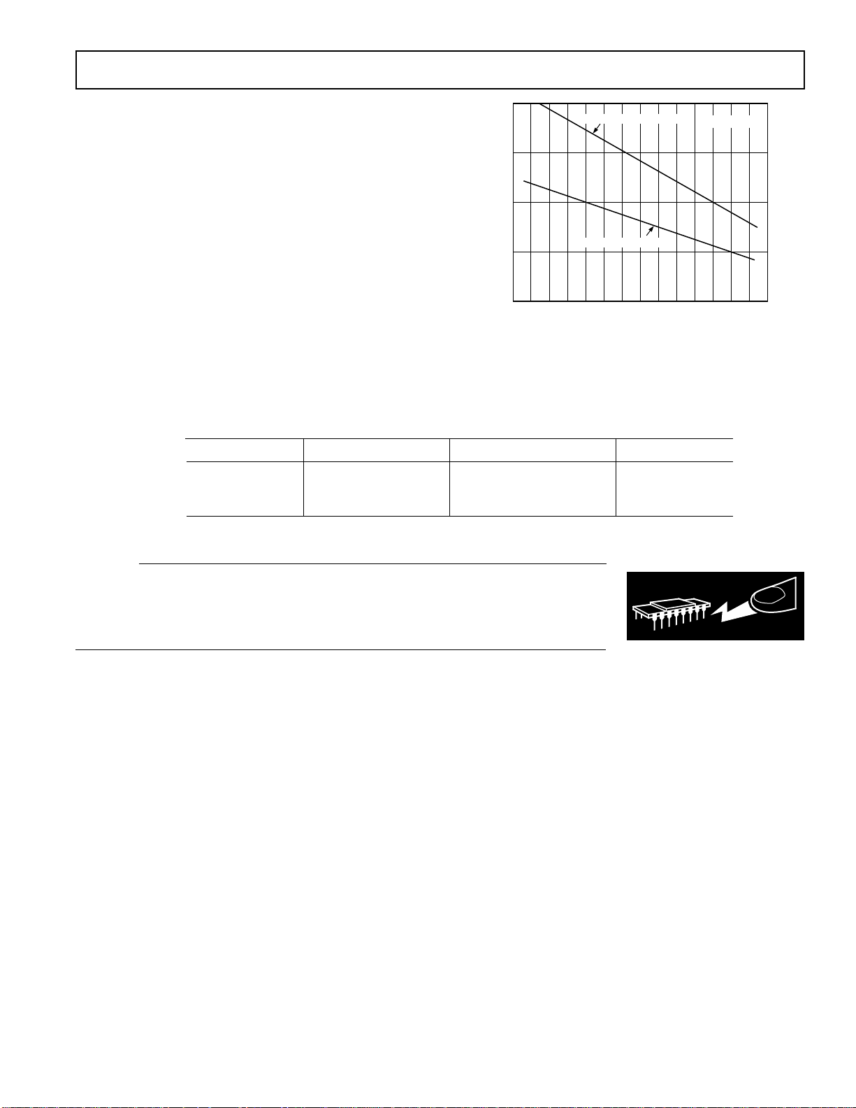
MAXIMUM POWER DISSIPATION – Watts
AMBIENT TEMPERATURE – °C
2.0
1.5
0
–50 90–40 –30 –20 –10 0 10 20 30 50 60 70 8040
1.0
0.5
8-PIN MINI-DIP PACKAGE
8-PIN SOIC PACKAGE
TJ = +150°C
WARNING!
ESD SENSITIVE DEVICE
ABSOLUTE MAXIMUM RATINGS
Supply Voltage . . . . . . . . . . . . . . . . . . . . . . . . . . . . . . . . +36 V
Internal Power Dissipation
2
1
Plastic Package (N) . . . . . . . . . . . . . . . . . . . . . . . . 1.3 Watts
Small Outline Package (R) . . . . . . . . . . . . . . . . . . . 0.9 Watts
Input Voltage (Common Mode) . . . . . . . . . . . . . . . . . . . . ±V
S
Differential Input Voltage . . . . . . . . . . . . . . . . . . . . . . . ±1.2 V
Output Short Circuit Duration
. . . . . . . . . . . . . . . . . . . . . . Observe Power Derating Curves
Storage Temperature Range N, R . . . . . . . . .–65°C to +125°C
Operating Temperature Range . . . . . . . . . . . . –40°C to +85°C
Lead Temperature Range (Soldering 10 sec) . . . . . . . . +300°C
NOTES
1
Stresses above those listed under “Absolute Maximum Ratings” may cause
permanent damage to the device. This is a stress rating only and functional
operation of the device at these or any other conditions above those indicated in the
operational section of this specification is not implied. Exposure to absolute
maximum rating conditions for extended periods may affect device reliability.
2
Specification is for device in free air:
8-Pin Plastic Package: θJA = 90°C/Watt
8-Pin SOIC Package: θJA = 160°C/Watt
ORDERING GUIDE
Model Temperature Range Package Description Package Option
AD823AN –40°C to +85°C 8-Pin Plastic DIP N-8
AD823AR –40°C to +85°C 8-Pin Plastic SOIC SO-8
AD823AR-REEL –40°C to +85°C SOIC on Reel SO-8
Figure 3. Maximum Power Dissipation vs. Temperature
CAUTION
ESD (electrostatic discharge) sensitive device. Electrostatic charges as high as 4000 V readily
accumulate on the human body and test equipment and can discharge without detection.
Although the AD823 features proprietary ESD protection circuitry, permanent damage may
occur on devices subjected to high energy electrostatic discharges. Therefore, proper ESD
precautions are recommended to avoid performance degradation or loss of functionality.
REV. 0
–5–
Page 6

AD823–Typical Characteristics
COMMON MODE VOLTAGE – Volts
0.1
INPUT BIAS CURRENT – pA
–16
100
10
1
1k
–12 4 8 12 16
VS = ±15V
–8 –4 0
80
70
60
50
40
UNITS
30
20
10
0
–200 200–150
–100 –50 0 50 100 150
INPUT OFFSET VOLTAGE – µV
VS = +5V
314 UNITS
s = 40µV
Figure 4. Typical Distribution of Input Offset Voltage
22
20
18
16
14
12
UNITS
10
8
6
4
2
0
–6 7–5
–4 –3 –2 3 4 5
INPUT OFFSET VOLTAGE DRIFT – µV/°C
VS = +5V
–55°C TO +125°C
103 UNITS
6–1012
100
90
80
70
60
50
UNITS
40
30
20
10
0
0
12345678910
INPUT BIAS CURRENT – pA
VS = +5V
317 UNITS
s = 0.4pA
Figure 7. Typical Distribution of Input Bias Current
10k
VS = +5V
V
= 0V
CM
1k
100
10
1
INPUT BIAS CURRENT – pA
0.1
0
25 50 75 100 125
TEMPERATURE – °C
Figure 5. Typical Distribution of Input Offset Voltage Drift
3
VS = +5V
–1
–2
INPUT BIAS CURRENT – pA
–3
Figure 6. Input Bias Current vs. Common-Mode Voltage
–4
2
1
0
–4–3–2–1012345
–5
COMMON MODE VOLTAGE – Volts
Figure 8. Input Bias Current vs. Temperature
Figure 9. Input Bias Current vs. Common-Mode Voltage
REV. 0–6–
Page 7

AD823
FREQUENCY – Hz
100
30
3
10 1M100 1k 10k 100k
10
VS = +5V
INPUT VOLTAGE NOISE – nV/
√
Hz
110
100
VS = ± 2.5V
90
80
OPEN-LOOP GAIN – dB
70
60
100
1k
LOAD RESISTANCE – Ω
10k
100k 500k
Figure 10. Open-Loop Gain vs. Load Resistance
1k
RL = 10kΩ
100
V
V
RL = 1kΩ
10
RL = 100Ω
OPEN-LOOP GAIN – k
1
0.1
–2.0 –0.5 0.5 1.0 2.5
–2.5
–1.5 –1.0 0 1.5 2.0
OUTPUT VOLTAGE – Volts
95
94
93
92
91
90
89
OPEN-LOOP GAIN – dB
88
87
86
–25 5 35 65 95 125
–55
TEMPERATURE – °C
VS = +5V
R
= 2kΩ
L
Figure 13. Open-Loop Gain vs. Temperature
100
80
60
40
20
OPEN-LOOP GAIN – dB
RL = 2kΩ
0
C
= 20pF
L
–20
100 100M1k 10k 100k 1M 10M
FREQUENCY – Hz
GAIN
PHASE
100
80
60
40
20
0
–20
PHASE MARGIN – Degrees
Figure 11. Open-Loop Gain vs. Output Voltage, VS = ±2.5 V
–40
–50
–60
VS = +3V
V
= 2Vp-p
OUT
R
= 100Ω
–70
L
–80
THD – dB
VS = ±2.5V
V
–90
–100
–110
Figure 12. Total Harmonic Distortion vs. Frequency
= 2Vp-p
OUT
R
= 1kΩ
L
100 100k
VS = ±15V
V
= 10Vp-p,
OUT
R
= 600Ω
L
1k 10k
FREQUENCY – Hz
RL = 600Ω
VS = +3V,
V
OUT
R
= 5kΩ
L
VS = +5V
V
= 2Vp-p
OUT
R
= 5kΩ
L
ALL
OTHERS
= 2Vp-p,
1M
Figure 14. Open-Loop Gain and Phase vs. Frequency
Figure 15. Input Voltage Noise vs. Frequency
REV. 0
–7–
Page 8

AD823–Typical Characteristics
FREQUENCY – Hz
20
70
60
90
80
30
40
50
CMRR – dB
10
VS = ±15V
100 1k 10k 100k 10M1M
VS = +5V
LOAD CURRENT – mA
0.01
1
10
0.1
OUTPUT SATURATION VOLTAGE – Volts
0.1
1 10 100
VS = +5V
V
OL
+25°C
VS – V
OH
+25°C
V
OL
+25°C
SUPPLY VOLTAGE – ±Volts
0
SUPPLY CURRENT – mA
0
4
2
10
8
5101520
6
+125°C
+25°C
–55°C
5
–55°C
G = +1
C
= 20pF
L
R
= 2kΩ
L
4
3
2
1
0
–1
–2
CLOSED-LOOP GAIN – dB
–3
–4
–5
0.3
+125°C
3.27 6.24 9.21 12.18 15.15 18.12 21.09 24.06 27.03 30
+27°C
FREQUENCY – MHz
Figure 16. Closed Loop Gain vs. Frequency
100
VS = +5V
GAIN = +1
10
1.0
OUTPUT RESISTANCE – Ω
0.1
0.01
100 1k 10k 100k 10M1M
Figure 17. Output Resistance vs. Frequency, VS = 5 V,
Gain = +1
10
VS = ±15V
8
C
= 20pF
– Volts
L
6
SHOWN
4
2
0
–2
–4
–6
–8
OUTPUT STEP SIZE FROM 0V TO V
–10
100 200 400 500 700600
Figure 18. Inverter Settling Time vs. Output Step Size
1%
300
FREQUENCY – Hz
1%
SETTLING TIME – ns
0.1%
0.1%
0.01%
0.01%
Figure 19. Common-Mode Rejection vs. Frequency
Figure 20. Output Saturation Voltage vs. Load Current
Figure 21. Quiescent Current vs. Supply Voltage
–8–
REV. 0
Page 9

AD823
100k
+3V
V
OUT
50pF
100k
50Ω
100k
V
IN
= 2.9V p-p
VS = +3V
V
IN
= 2.9Vp-p
G = –1
10µs
500mV
100
90
80
70
60
50
40
30
20
POWER SUPPLY REJECTION – dB
10
0
100 1k 10k
–PSRR
FREQUENCY – Hz
+PSRR
100k
VS = +5V
1M 10M
Figure 22. Power Supply Rejection vs. Frequency
30
RL = 2kΩ
G = +1
20
VS = ±15V
10
OUTPUT VOLTAGE – Vp-p
0
10k
VS = +5V
VS = +3V
100k 1M 10M
FREQUENCY – Hz
21
VS = +5V
R
S
C
L
V
18
15
12
9
6
SERIES RESISTANCE – Ω
3
0
0
f
= 20°
M
12345678910
CAPACITOR – pF 3 1000
IN
f
= 45°
M
Figure 25. Capacitive Load vs. Series Resistance
–30
VS = +5V
–40
–50
–60
–70
–80
–90
CROSSTALK – dB
–100
–110
–120
–130
1k
10k 100k 1M
FREQUENCY – Hz
10M
REV. 0
Figure 23. Large Signal Frequency Response
RL = 100kΩ
= 50pF
C
L
V
= +3V
3V
GND
500mV
S
200µs
Figure 24. Output Swing, VS = + 3 V, G = +1
Figure 26. Crosstalk vs. Frequency
Figure 27. Output Swing, VS = +3 V, G = –1
–9–
Page 10

AD823–Typical Characteristics
VS = +5V
G = +1
R
L
= 2kΩ
C
L
= 470pF
200ns
50mV
GND
5V
500mV
RL = 300Ω
= 50pF
C
L
= RG = 2kΩ
R
F
200µs
Figure 28. Output Swing, VS = +5 V, G = –1
VS = +3V
= 100mV STEP
V
IN
G =+1
1.55V
VS = ±15V
V
= 20Vp-p
IN
G = 1
604Ω
20µs
50pF
5V
+15V
20kHz, 20Vp-p
–15V
Figure 31. Output Swing, VS = ±15 V, G = +1
5V
RL = 2kΩ
= 50pF
C
L
1.45V
25mV
50ns
Figure 29. Pulse Response, VS = +3 V, G = +1
5V
VS = +5V
G =+2
= 2kΩ
R
L
= 50pF
C
L
GND
500mV
100ns
Figure 30. Pulse Response, VS = +5 V , G = +2
GND
500mV
100ns
Figure 32. Pulse Response, VS = +5 V, G = +1
Figure 33. Pulse Response, VS = +5 V, G = +1, CL = 470 pF
–10–
REV. 0
Page 11

10V
–10V
RL = 100kΩ
= 50pF
C
L
AD823
5V
Figure 34. Pulse Response, VS = ±15 V, G = +1
THEORY OF OPERATION
This AD823 is fabricated on Analog Devices’ proprietary
complementary bipolar (CB) process that enables the construction of pnp and npn transistors with similar f
s in the 600 MHz
T
to 800 MHz region. In addition, the process also features
N-channel JFETs, which are used in the input stage of the AD823.
These process features allow the construction of high frequency,
low distortion op amps with picoampere input currents. This
design uses a differential-output input stage to maximize bandwidth and headroom (see Figure 35). The smaller signal swings
required on the S1P, S1N outputs reduce the effect of nonlinear
currents due to junction capacitances and improve the distortion
performance. With this design harmonic distortion of better
than –91 dB @ 20 kHz into 600 Ω with V
= 4 V p-p on a
OUT
single 5 volt supply is achieved. The complementary commonemitter design of the output stage provides excellent load drive
without the need for emitter followers, thereby improving the
output range of the device considerably with respect to conventional op amps. The AD823 can drive 20 mA with the outputs
within 0.6 V of the supply rails. The AD823 also offers outstanding precision for a high speed op amp. Input offset voltages
500ns
of 1 mV max and offset drift of 2 µV/°C are achieved through
the use of Analog Devices’ advanced thin-film trimming
techniques.
A “Nested Integrator” topology is used in the AD823 (see smallsignal schematic shown in Figure 36). The output stage can be
modeled as an ideal op amp with a single-pole response and a
unity-gain frequency set by transconductance g
C2. R1 is the output resistance of the input stage; g
and capacitor
m2
is the in-
m
put transconductance. C1 and C5 provide Miller compensation
for the overall op amp. The unity gain frequency will occur at
g
/C5. Solving the node equations for this circuit yields:
m
V
OUT
=
Vi
sR1[ C 1(A2 +1)] +1)
(
A0
× s
g
C 2
m2
+ 1
where:
A0 = g
A2 = g
R2R1 (Open Loop Gain of Op Amp)
mgm2
R2 (Open Loop Gain of Output Stage)
m2
REV. 0
V
CC
V
INP
V
INN
V
EE
R42 R37
J1
I1
+ 0.3V
V
Q72
J6
S1P
V
Q48
Q53
C6
R33
BE
CC
V1
Q61
Q46
S1N
Q35
I2
R43
Q43
I5
Q58
R44
Q21
Q62 Q60
I3
Q56
R28
Q55
Q49
Q54
V
B
Q52
Q44
I6
A=1
Q57
A=19
Q18
I4
Q59
A=1
C2
V
OUT
C1
Q17
A=19
Figure 35. Simplified Schematic
–11–
Page 12

AD823
GND
10
90
100
0%
1V
2µs
1V
The first pole in the denominator is the dominant pole of the
amplifier, and occurs at about 18 Hz. This equals the input
stage output impedance R1 multiplied by the Miller-multiplied
value of C1. The second pole occurs at the unity-gain bandwidth of the output stage, which is 23 MHz. This type of architecture allows more open loop gain and output drive to be
obtained than a standard two-stage architecture would allow.
OUTPUT IMPEDANCE
The low frequency open loop output impedance of the
common-emitter output stage used in this design is approximately 30 kΩ. While this is significantly higher than a typical
emitter follower output stage, when connected with feedback
the output impedance is reduced by the open loop gain of the
op amp. With 109 dB of open loop gain the output impedance
is reduced to less than 0.2 Ω. At higher frequencies the output
impedance will rise as the open loop gain of the op amp drops;
however, the output also becomes capacitive due to the integrator capacitors C1 and C2. This prevents the output impedance
from ever becoming excessively high (see Figure 17), which can
cause stability problems when driving capacitive loads. In fact,
the AD823 has excellent cap-load drive capability for a high frequency op amp. Figure 33 shows the AD823 connected as a follower while driving 470 pF direct capacitive load. Under these
conditions the phase margin is approximately 20°. If greater
phase margin is desired a small resistor can be used in series
with the output to decouple the effect of the load capacitance
from the op amp (see Figure 25). In addition, running the part
at higher gains will also improve the capacitive load drive capability of the op amp.
APPLICATION NOTES
INPUT CHARACTERISTICS
In the AD823, n-channel JFETs are used to provide a low
offset, low noise, high impedance input stage. Minimum input
common-mode voltage extends from 0.2 V below –V
less than +V
. Driving the input voltage closer to the positive
S
to 1 V
S
rail will cause a loss of amplifier bandwidth and increased
common-mode voltage error.
The AD823 does not exhibit phase reversal for input voltages
up to and including +V
AD823 voltage follower to a 0 V to +5 V (+V
. Figure 37a shows the response of an
S
) square wave
S
input. The input and output are superimposed. The output
polarity tracks the input polarity up to +V
—no phase reversal.
S
The reduced bandwidth above a 4 V input causes the rounding
of the output wave form. For input voltages greater than +V
, a
S
resistor in series with the AD823’s plus input will prevent phase
reversal, at the expense of greater input voltage noise. This is illustrated in Figure 37b.
S1N
VI
g
m
g
m
R1
S1P
VI
C5
R1
C1
V
C2
R2
g
m2
Figure 36. Small Signal Schematic
OUT
a. Response with RP = 0; VIN from 0 to V
+V
GND
1V
100
90
S
10
0%
1V
V
IN
1V
R
P
AD823
b. VIN = 0 to +VS + 200 mV; V
10µs
+5V
= 0 to +VS; RP = 49.9 k
OUT
S
V
OUT
Ω
Figure 37. AD823 Input Response
–12–
REV. 0
Page 13

AD823
Since the input stage uses n-channel JFETs, input current during normal operation is negative; the current flows out from the
input terminals. If the input voltage is driven more positive than
+V
– 0.4 V, the input current will reverse direction as internal
S
device junctions become forward biased. This is illustrated in
Figure 6.
A current limiting resistor should be used in series with the input of the AD823 if there is a possibility of the input voltage exceeding the positive supply by more than 300 mV, or if an input
voltage will be applied to the AD823 when ± V
= 0. The ampli-
S
fier will be damaged if left in that condition for more than 10
seconds. A 1 kΩ resistor allows the amplifier to withstand up to
10 volts of continuous overvoltage, and increases the input voltage noise by a negligible amount.
Input voltages less than –V
are a completely different story.
S
The amplifier can safely withstand input voltages 20 volts below
the minus supply voltage as long as the total voltage from the
positive supply to the input terminal is less than 36 volts. In
addition, the input stage typically maintains picoamp level input
currents across that input voltage range.
The AD823 is designed for 16 nV/√
Hz wideband input voltage
noise and maintains low noise performance to low frequencies
(refer to Figure 15). This noise performance, along with the
AD823’s low input current and current noise means that the
AD823 contributes negligible noise for applications with source
resistances greater than 10 kΩ and signal bandwidths greater
than 1 kHz.
OUTPUT CHARACTERISTICS
The AD823’s unique bipolar rail-to-rail output stage swings
within 25 mV of the supplies with no external resistive load. The
AD823’s approximate output saturation resistance is 25 Ω
sourcing and sinking. This can be used to estimate output saturation voltage when driving heavier current loads. For instance,
when driving 5 mA, the saturation voltage to the rails will be approximately 125 mV.
If the AD823’s output is driven hard against the output saturation voltage, it will recover within 250 ns of the input returning
to the amplifier’s linear operating region.
A/D Driver
The rail-to-rail output of the AD823 makes it useful as an A/D
driver in a single supply system. Because it is a dual op amp, it
can be used to drive both the analog input of the A/D along with
its reference input. The high impedance FET input of the
AD823 is well suited for minimally loading of high output impedance devices.
Figure 38 shows a schematic of an AD823 being used to drive
both the input and reference input of an AD1672, a 12-bit
3 MSPS single supply A/D converter. One amplifier is configured as a unity gain follower to drive the analog input of the
AD1672 which is configured to accept an input voltage that
ranges from 0 to 2.5 V.
+5VA +5VD +5VD
V
REF
(1.25V)
+5VA
0.1µF
8
2
1
3
V
IN
10µF
10µF
49.9Ω
AD823
5
7
6
4
1k
1k
CLOCK
0.1
µF
+VCC+V
20
REFOUT
21
AIN1
22
AIN2
AD1672
23
REFIN
24
IN COM
25
NCOMP2
26
NCOMP1
27
ACOM
16
REF
COM
19 18
28 19
COM
0.1µF10
DD
15
13
14
12
11
10
9
8
7
6
5
4
3
2
1
D
µF
OTR
BIT1 (MSB)
BIT2
BIT3
BIT4
BIT5
BIT6
BIT7
BIT8
BIT9
BIT10
BIT11
BIT12 (LSB)
0.1µF
Figure 38. AD823 Driving Input and Reference of the
AD1672, a 12-Bit 3 MSPS A/D Converter
The other amplifier is configured as a gain of two to drive the
reference input from a 1.25 V reference. Although the AD1672
has its own internal reference, there are systems that require
greater accuracy than the internal reference provides. On the
other hand, if the AD1672 internal reference is used, the second
AD823 amplifier can be used to buffer the reference voltage for
driving other circuitry while minimally loading the reference
source.
The circuit was tested with a 500 kHz sine wave input that was
heavily low pass filtered (60 dB) to minimize the harmonic content at the input to the AD823. The digital output of the
AD1672 was analyzed by performing an FFT.
During the testing, it was observed that at 500 kHz, the output
of the AD823 cannot go below about 350 mV (operating with
negative supply at ground) without seriously degrading the second harmonic distortion. Another test was performed with a
200 Ω pull-down resistor to ground that allowed the output to
go as low as 200 mV without seriously affecting the second harmonic distortion. There was, however, a slight increase in the
third harmonic term with the resistor added, but it was still less
than the second harmonic.
REV. 0
–13–
Page 14

AD823
1/2
AD823
C3
0.1µF
+5V
C4
0.1µF
V
OUT
V
IN
C1
28pF
–5V
C2
56pF
R1
20kR220k
50pF
Figure 39 is an FFT plot of the results of driving the AD1672
with the AD823 with no pull-down resistor. The input amplitude was 2.15 V p-p and the lower voltage excursion was
350 mV. The input frequency was 490 kHz, which was chosen
to spread the location of the harmonics.
The distortion analysis is important for systems requiring good
frequency domain performance. Other systems may require
good time domain performance. The noise and settling time
performance of the AD823 will provide the necessary information for its applicability for these systems.
1
V
= 2.15Vp-p
IN
G = +1
FI = 490kHz
2
7
8
3
5
15dB/DIV
4
9
6
Figure 39. FFT of AD1672 Output Driven by AD823
3 Volt, Single Supply Stereo Headphone Driver
The AD823 exhibits good current drive and THD+N performance, even at 3 V single supplies. At 20 kHz, total harmonic
distortion plus noise (THD+N) equals –62 dB (0.079%) for a
300 mV p-p output signal. This is comparable to other single
supply op amps which consume more power and cannot run on
3 V power supplies.
In Figure 40, each channel’s input signal is coupled via a 1 µF
Mylar capacitor. Resistor dividers set the dc voltage at the noninverting inputs so that the output voltage is midway between
the power supplies (+1.5 V). The gain is 1.5. Each half of the
AD823 can then be used to drive a headphone channel. A 5 Hz
high-pass filter is realized by the 500 µF capacitors and the
headphones, which can be modeled as 32 ohm load resistors to
ground. This ensures that all signals in the audio frequency
range (20 Hz–20 kHz) are delivered to the headphones.
+3V
0.1µF0.1µF
L
R
CHANNEL 1
CHANNEL 2
95.3kΩ
1µF
MYLAR
95.3k
1µF
MYLAR
95.3k
47.5k
47.5k
3
2
10k
10k
AD823
6
AD823
5
1/2
1/2
8
4
4.99k
4.99k
1
1
7
+
500µF
HEADPHONES
32Ω IMPEDANCE
500µF
+
Figure 40. 3 Volt Single Supply Stereo Headphone Driver
Second Order Low-Pass Filter
Figure 41 depicts the AD823 configured as a second order
Butterworth low-pass filter. With the values as shown, the corner frequency will be 200 kHz. The equations for component
selection are shown below:
R1 = R2 = user selected (typical values: 10 kΩ to 100 kΩ).
C1( farads ) =
2 πf
1.414
cutoff
R1
; C2 =
2 πf
0.707
cutoff
R1
Figure 41. Second Order Low-Pass Filter
A plot of the filter is shown below; better than 50 dB of high frequency rejection is provided.
–14–
REV. 0
Page 15

AD823
10
90
100
0%
2V
2V
200µs
2V
A
B
C
3
2
1
8
4
0.01µF
V
IN
+V
S
1/2
AD823
HALF-WAVE
RECTIFIED OUTPUT
FULL-WAVE
RECTIFIED OUTPUT
A1
R2
100kΩ
R1
100kΩ
6
5
7
1/2
AD823
A2
A
B
C
0
–10
VDB – V
–20
–30
–40
–50
HIGH FREQUENCY REJECTION – dB
–60
1k
10k 100k
FREQUENCY – Hz
OUT
1M
10M 100M
Figure 42. Frequency Response of Filter
Single-Supply Half-Wave and Full-Wave Rectifiers
An AD823 configured as a unity gain follower and operated
with a single supply can be used as a simple half-wave rectifier.
The AD823’s inputs maintain picoamp level input currents even
when driven well below the minus supply. The rectifier puts that
behavior to good use, maintaining an input impedance of over
11
10
Ω for input voltages from 1 volt from the positive supply to
20 volts below the negative supply.
The full- and half-wave rectifier shown in Figure 43 operates as
follows: when V
is above ground, R1 is bootstrapped through
IN
the unity gain follower A1 and the loop of amplifier A2. This
forces the inputs of A2 to be equal, thus no current flows
through R1 or R2, and the circuit output tracks the input. When
V
is below ground, the output of A1 is forced to ground. The
IN
noninverting input of amplifier A2 sees the ground level output
of A1, therefore, A2 operates as a unity gain inverter. The out-
put at node C is then a full-wave rectified version of the input.
Node B is a buffered half-wave rectified version of the input.
Input voltage supply to ±18 volts can be rectified, depending on
the voltage supply used.
Figure 43. Single Supply Half- and Full-Wave Rectifier
REV. 0
–15–
Page 16

AD823
OUTLINE DIMENSIONS
Dimensions shown in inches and (mm).
8-Lead Plastic DIP
(N-8)
58
0.25
4
0.033
(0.84)
NOM
(6.35)
0.035±0.01
(0.89±0.25)
0.18±0.03
(4.57±0.76)
SEATING
PLANE
PIN 1
0.165±0.01
(4.19±0.25)
0.125
(3.18)
MIN
0.018±0.003
1
(0.46±0.08)
0.39 (9.91) MAX
0.10
(2.54)
BSC
8-Lead Plastic SOIC
(SO-8)
0.31
(7.87)
0.30 (7.62)
REF
0.011±0.003
(0.28±0.08)
15
°
0
°
C2035–7.5–5/95
0.0098 (0.25)
0.0040 (0.10)
PIN 1
8
1
0.1968 (5.00)
0.1890 (4.80)
0.0500
(1.27)
BSC
5
4
0.0192 (0.49)
0.0138 (0.35)
0.1574 (4.00)
0.1497 (3.80)
0.2440 (6.20)
0.2284 (5.80)
0.0688 (1.75)
0.0532 (1.35)
0.0098 (0.25)
0.0075 (0.19)
8°
0°
0.0196 (0.50)
0.0099 (0.25)
0.0500 (1.27)
0.0160 (0.41)
x 45°
–16–
PRINTED IN U.S.A.
REV. 0
 Loading...