

Page 1
Precision Gain of 5
Instrumentation Amplifier
AD8225
FEATURES
No External Components Required
Highly Stable, Factory Trimmed Gain of 5
Low Power, 1.2 mA Max Supply Current
Wide Power Supply Range (1.7 V to 18 V)
Single- and Dual-Supply Operation
Excellent Dynamic Performance
High CMRR
86 dB Min @ DC
80 dB Min to 10 kHz
Wide Bandwidth
900 kHz
4 V to 36 V Single Supply
High Slew Rate
5 V/s Min
Outstanding DC Precision
Low Gain Drift
5 ppm/C Max
Low Input Offset Voltage
150 V Max
Low Offset Drift
2 V/C Max
Low Input Bias Current
1.2 nA Max
APPLICATIONS
Patient Monitors
Current Transmitters
Multiplexed Systems
4 to 20 mA Converters
Bridge Transducers
Sensor Signal Conditioning
FUNCTIONAL BLOCK DIAGRAM
NC
–IN
+IN
–V
140
130
120
110
100
90
HIGH PERFORMANCE IN AMP
80
CMRR – dB
70
60
50
40
30
1 100k10
@ GAIN OF 5
AD8225
1
2
3
4
S
NC = NO CONNECT
100 1k 10k
FREQUENCY – Hz
8
NC
7
+V
S
6
V
OUT
5
REF
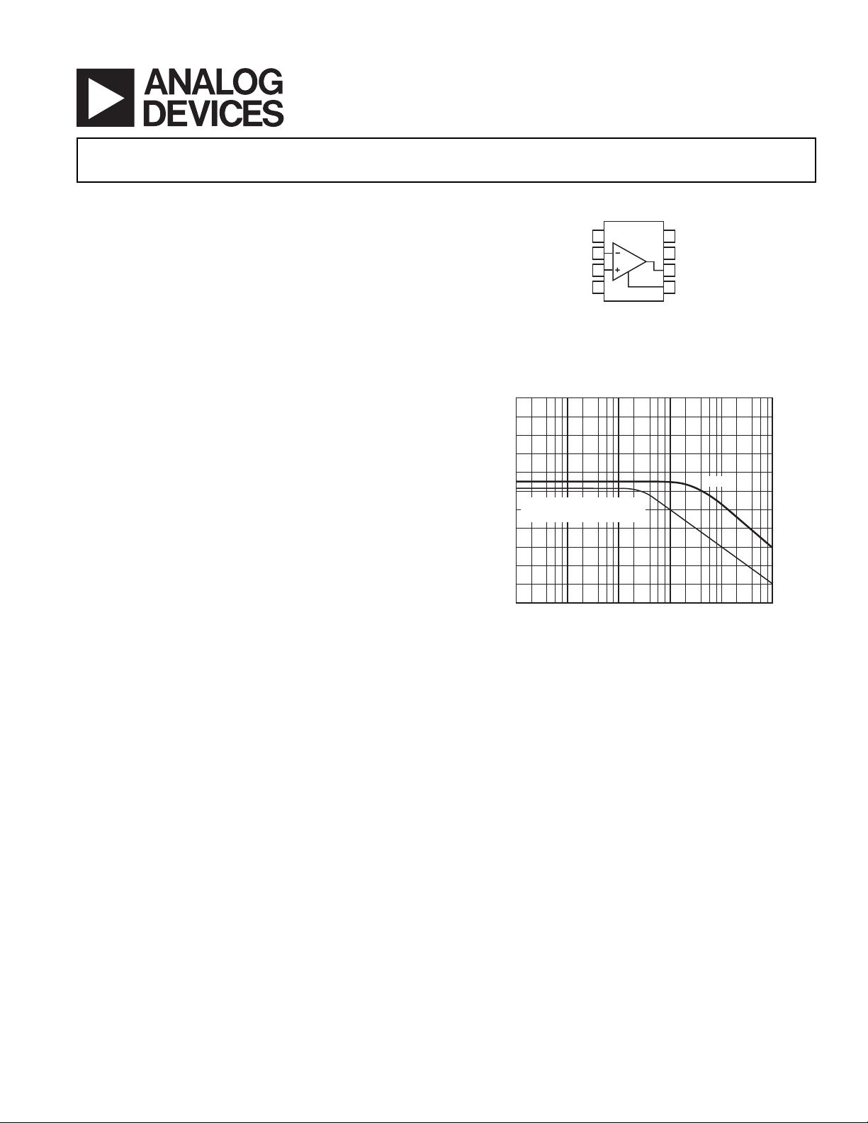
Figure 1. Typical CMRR vs. Frequency
AD8225
GENERAL DESCRIPTION
The AD8225 is an instrumentation amplifier with a fixed gain
of 5, which sets new standards of performance. The superior
CMRR of the AD8225 enables rejection of high frequency
common-mode voltage (80 dB Min @ 10 kHz). As a result,
higher ambient levels of noise from utility lines, industrial
equipment, and other radiating sources are rejected. Extended
CMV range enables the AD8225 to extract low level differential
signals in the presence of high common-mode dc voltage levels
even at low supply voltages.
Ambient electrical noise from utility lines is present at 60 Hz
and harmonic frequencies. Power systems operating at 400 Hz
create high noise environments in aircraft instrument clusters.
Good CMRR performance over frequency is necessary if power
system generated noise is to be rejected. The dc to 10 kHz
REV. A
Information furnished by Analog Devices is believed to be accurate and
reliable. However, no responsibility is assumed by Analog Devices for its
use, nor for any infringements of patents or other rights of third parties that
may result from its use. No license is granted by implication or otherwise
under any patent or patent rights of Analog Devices. Trademarks and
registered trademarks are the property of their respective companies.
CMRR performance of the AD8225 rejects noise from utility
systems, motors, and repair equipment on factory floors, switching power supplies, and medical equipment.
Low input bias currents combined with a high slew rate of 5 V/µs
make the AD8225 ideally suited for multiplexed applications.
The AD8225 provides excellent dc precision, with maximum
input offset voltage of 150 µV and drift of 2 µV/°C. Gain drift is
5ppm/°C or less.
Operating on either single or dual supplies, the fixed gain of 5
and wide input common-mode voltage range make the AD8225
well suited for patient monitoring applications.
The AD8225 is packaged in an 8-lead SOIC package and is
specified over the standard industrial temperature range, –40°C
to +85°C.
One Technology Way, P.O. Box 9106, Norwood, MA 02062-9106, U.S.A.
Tel: 781/329-4700 www.analog.com
Fax: 781/326-8703 © 2003 Analog Devices, Inc. All rights reserved.
Page 2

AD8225–SPECIFICATIONS
(TA = 25C, VS = 15 V, RL = 2 k, unless otherwise noted.)
Parameter Conditions Min Typ Max Unit
GAIN
Gain 5V/V
Gain Error –0.1 +0.05 +0.1 %
Nonlinearity 2 10 ±ppm
vs. Temperature 1 5 ±ppm/°C
OFFSET VOLTAGE (RTI)
Offset Voltage 50 150 ±µV
vs. Temperature 0.3 2 ±µV/°C
vs. Supply (PSRR) 90 100 dB
INPUT
Input Operating Impedance
储
Differential 10
Common Mode 10
Input Voltage Range –V
+ 1.6 +VS – 1.0 V
S
2GΩ储pF
储
2GΩ储pF
(Common-Mode)
vs. Temperature –V
+ 2.2 +VS – 1.2 V
S
Input Bias Current 0.5 1.2 nA
vs. Temperature 3 pA/°C
Input Offset Current 0.15 0.5 nA
vs. Temperature 1.5 pA/°C
Common-Mode Rejection Ratio 86 94 dB
= T
T
A
MIN
to T
MAX
83 dB
f = 10 kHz* 80 dB
OUTPUT
Operating Voltage Range RL = 2 kΩ –VS + 1.4 +VS – 1.4 V
vs. Temperature –V
Operating Voltage Range R
= 10 kΩ –VS + 1.0 +VS – 1.1 V
L
vs. Temperature –V
+ 1.5 +VS – 1.6 V
S
+ 1.2 +VS – 1.0 V
S
Short Circuit Current 18 mA
DYNAMIC RESPONSE
Small Signal –3 dB Bandwidth 900 kHz
Full Power Bandwidth V
= 20 V p-p 75 kHz
OUT
Settling Time (0.01%) 10 V Step 3.4 µs
Settling Time (0.001%) 10 V Step 4.8 µs
Slew Rate 5 V/µs
NOISE (RTI)
Voltage 0.1 Hz to 10 Hz 1.5 µV p-p
Spectral Density, 1 kHz 45 nV/√Hz
Current 0.1 Hz to 10 Hz 4 pA p-p
Spectral Density, 1 kHz 50 fA/√Hz
REFERENCE INPUT
R
IN
I
IN
Voltage Range –V
V
, V
IN+
= 0 18 kΩ
REF
60 µA
+ 1.4 +VS – 1.4 V
S
Gain to Output 0.999 1 1.001
POWER SUPPLY
Operating Range 1.7 18 ±V
Quiescent Current 1.05 1.2 mA
TEMPERATURE RANGE
For Specified Performance –40 +85 °C
*Pin 1 connected to Pin 4. See Applications section.
Specifications subject to change without notice.
REV. A–2–
Page 3

AD8225
SPECIFICATIONS
(TA = 25C, VS = 5 V, RL = 2 k, unless otherwise noted.)
Parameter Conditions Min Typ Max Unit
GAIN
Gain 5V/V
Gain Error –0.1 +0.05 +0.1 %
Nonlinearity 2 10 ±ppm
vs. Temperature 1 5 ±ppm/°C
VOLTAGE OFFSET (RTI)
Offset Voltage 125 325 ±µV
vs. Temperature 2 ±µV/°C
vs. Supply 90 100 dB
INPUT
Input Operating Impedance
Differential 10
Common-Mode 10
Input Operating Voltage Range –V
vs. Temperature –V
+ 1.6 +VS – 1.0 V
S
+ 2.1 +VS – 1.5 V
S
储
2GΩ储pF
储
2GΩ储pF
Input Bias Current 0.5 1.2 nA
vs. Temperature 3 pA/°C
Input Offset Current 0.15 0.5 nA
vs. Temperature 1.5 pA/°C
Common-Mode Rejection Ratio 86 94 dB
= T
T
A
MIN
to T
MAX
83 dB
f = 10 kHz* 80 dB
OUTPUT
Operating Voltage Range RL = 2 kΩ –VS + 0.9 +VS – 1.0 V
vs. Temperature –V
Operating Voltage Range R
= 10 kΩ –VS + 0.8 +VS – 1.0 V
L
vs. Temperature –V
+ 1.0 +VS – 1.2 V
S
+ 0.9 +VS – 1.0 V
S
Short Circuit Current 18 mA
DYNAMIC RESPONSE
Small Signal –3 dB Bandwidth 900 kHz
Full Power Bandwidth V
= 7.8 V p-p 170 kHz
OUT
Settling Time (0.01%) 7 V Step 3 µs
Settling Time (0.001%) 7 V Step 4.3 µs
Slew Rate 5 V/µs
NOISE (RTI)
Voltage 0.1 Hz to 10 Hz 1.5 µV p-p
Spectral Density, 1 kHz 45 nV/√Hz
Current 0.1 Hz to 10 Hz 4 pA p-p
Spectral Density, 1 kHz 50 fA/√Hz
REFERENCE INPUT
R
IN
I
IN
V
, V
INT
= 0 60 µA
REF
Voltage Range –V
+ 0.9 +VS – 1.0 V
S
18 kΩ
Gain to Output 0.999 1 1.001
POWER SUPPLY
Operating Range 1.7 18 ±V
Quiescent Current 1.05 1.2 mA
TEMPERATURE RANGE
For Specified Performance –40 +85 °C
*Pin 1 connected to Pin 4. See Applications section.
Specifications subject to change without notice.
REV. A
–3–
Page 4

AD8225
SPECIFICATIONS
(TA = 25C, VS = 5 V, RL = 2 k, unless otherwise noted.)
Parameter Conditions Min Typ Max Unit
GAIN
Gain 5V/V
Gain Error –0.1 +0.05 +0.1 %
Nonlinearity 2 10 ±ppm
vs. Temperature 1 5 ±ppm/°C
OFFSET VOLTAGE (RTI)
Offset Voltage 150 375 ±µV
vs. Temperature 2 ±µV/°C
vs. Supply 90 100 dB
INPUT
Input Operating Impedance
Differential 10
Common Mode 10
Input Voltage Range 1.6 V
储
2GΩ储pF
储
2GΩ储pF
– 1.05 V
S
(Common-Mode)
vs. Temperature 1.7 V
– 1.0 V
S
Input Bias Current 0.5 1.2 nA
vs. Temperature 3 pA/°C
Input Offset Current 0.15 0.5 nA
vs. Temperature 1.5 pA/°C
Common-Mode Rejection Ratio 86 94 dB
= T
T
A
MIN
to T
MAX
83 dB
f = 10 kHz* 80 dB
OUTPUT
Operating Voltage Range RL = 2 kΩ 0.8 VS – 1.05 V
vs. Temperature 0.9 V
Operating Voltage Range R
= 10 kΩ 0.8 VS – 1.0 V
L
vs. Temperature 0.9 V
– 1.2 V
S
– 1.0 V
S
Short Circuit Current 18 mA
DYNAMIC RESPONSE
Small Signal –3 dB Bandwidth 900 kHz
Full Power Bandwidth V
= 3.2 V p-p 420 kHz
OUT
Settling Time (0.01%) 2 V Step 3.3 µs
Settling Time (0.001%) 2 V Step 5.1 µs
Slew Rate 5 V/µs
NOISE (RTI)
Voltage 0.1 Hz to 10 Hz 1.5 µV p-p
Spectral Density, 1 kHz 45 nV/√Hz
Current 0.1 Hz to 10 Hz 4 pA p-p
Spectral Density, 1 kHz 50 fA/√Hz
REFERENCE INPUT
R
IN
I
IN
Voltage Range 0.4 V
18 kΩ
60 µA
– 0.9 V
S
Gain to Output 0.999 1 1.001
POWER SUPPLY
Operating Range 3.4 36 V
Quiescent Current 1.05 1.2 mA
TEMPERATURE RANGE
For Specified Performance –40 +85 °C
*Pin 1 connected to Pin 4. See Applications section.
Specifications subject to change without notice.
REV. A–4–
Page 5
AD8225
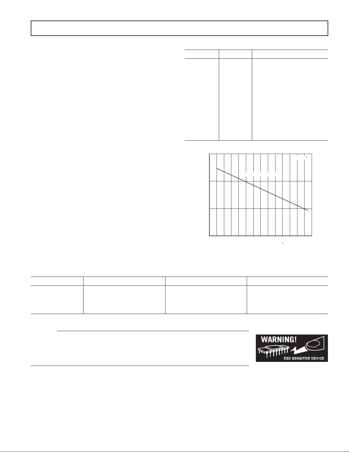
AMBIENT TEMPERATURE – C
1.5
1.0
0
–5080–40
POWER DISSIPATION – W
–30
–20
–10 0 10 203040506070
0.5
90
TJ = 150 C
8-LEAD SOIC PACKAGE
ABSOLUTE MAXIMUM RATINGS*
Supply Voltage . . . . . . . . . . . . . . . . . . . . . . . . . . . . . . . . ± 18 V
Internal Power Dissipation . . . . . . . . . . . . . . . . . . . . 650 mW
Input Voltage (Common-Mode) . . . . . . . . . . . . . . . . . . . . ±V
S
Differential Input Voltage . . . . . . . . . . . . . . . . . . . . . . . ±25 V
Output Short Circuit Duration . . . . . . . . . . . . . . . . Indefinite
Storage Temperature . . . . . . . . . . . . . . . . . . –65ºC to +125ºC
Operating Temperature Range . . . . . . . . . . . –40ºC to +85ºC
Lead Temperature Range (10 sec Soldering) . . . . . . . . . 300ºC
*Stresses above those listed under Absolute Maximum Ratings may cause perma-
nent damage to the device. This is a stress rating only and functional operation of
the device at these or any other conditions above those indicated in the operational
section of this specification is not implied. Exposure to absolute maximum rating
conditions for extended periods may affect device reliability.
PIN FUNCTION DESCRIPTIONS
Pin Number Mnemonic Function
1NCMay be Connected to Pin 4 to
Balance C
IN
2 –IN Inverting Input
3 +IN Noninverting Input
4 –V
S
Negative Supply Voltage
5 REF Connect to Desired Output
CMV
6V
7+V
OUT
S
Output
Positive Supply Voltage
8NC
Figure 2. Maximum Power Dissipation vs. Temperature
ORDERING GUIDE
Model Temperature Range Package Description Package Options
AD8225AR –40ºC to +85ºC 8-Lead SOIC RN-8
AD8225AR-REEL –40ºC to +85ºC 8-Lead SOIC 13" REEL
AD8225AR-REEL7 –40ºC to +85ºC 8-Lead SOIC 7" REEL
AD8225-EVAL Evaluation Board RN-8
CAUTION
ESD (electrostatic discharge) sensitive device. Electrostatic charges as high as 4000 V readily
accumulate on the human body and test equipment and can discharge without detection. Although the
AD8225 features proprietary ESD protection circuitry, permanent damage may occur on devices
subjected to high energy electrostatic discharges. Therefore, proper ESD precautions are recommended
to avoid performance degradation or loss of functionality.
REV. A
–5–
Page 6

AD8225–Typical Performance Characteristics
(TA = 25C, RL = 2 k, VS = 15 V, unless otherwise noted.)
50
45
40
35
30
25
20
% OF UNITS
15
10
5
0
–140 120–120
–80 –40 –20 0 20 40 60 80
–100 –60 100
INPUT OFFSET VOLTAGE – V
LOT SIZE = 3775
TPC 1. Typical Distribution of Input Offset Voltage,
V
= ±15 V
S
50
45
40
35
30
25
20
% OF UNITS
15
10
5
0
–200 800–100
0 100 200 300 400 500 700
INPUT BIAS CURRENT – pA
LOT SIZE = 7550
600
TPC 2. Typical Distribution of Input Bias Current,
V
= ±15 V
S
250
200
150
+BIAS CURRENT
100
50
BIAS CURRENT – pA
0
–50
–60 100–40
–BIAS CURRENT
–20 0 20 40 60 80
TEMPERATURE – C
TPC 4. Bias Current vs. Temperature
8
6
4
2
CHANGE IN OFFSET VOLTAGE – V
0
051
234
WARM-UP TIME – Min
TPC 5. Offset Voltage vs. Warm-Up Time
50
45
40
35
30
25
20
% OF UNITS
15
10
5
0
–500 400–400
–300 –100 0 100 200 300
–200
INPUT OFFSET CURRENT – pA
LOT SIZE = 3775
TPC 3. Typical Distribution of Input Offset Current,
= ±15 V
V
S
1000
100
VOLTA G E NOISE DENSITY – nV/ Hz
0
1 100k10
100 1k 10k
FREQUENCY – Hz
TPC 6. Voltage Noise Spectral Density vs. Frequency (RTI)
REV. A–6–
Page 7

1000
FREQUENCY – Hz
130
110
30
1 100k10
CMR – dB
100 1k 10k
90
70
50
120
100
80
60
40
TEMPERATURE – C
0.10
–0.10
–40 100–20
CMRR DRIFT – ppm/ C
020406080
0.08
–0.02
–0.04
–0.06
–0.08
0.04
0
0.06
0.02
OUTPUT VOLTAGE – V
15
–15
–1515–10
COMMON-MODE VOLTAGE – V
–5
0
5
10
10
5
0
–5
–10
VS = 15V
VS = 5V
100
VOLTA G E NOISE DENSITY – nV/ Hz
0
1 10k10
AD8225
100 1k
FREQUENCY – Hz
TPC 7. Input Current Noise Spectral Density vs.
Frequency
4
3
100
90
2
1
0
–1
NOISE – RTI – V
10
–2
0
–3
–4
0
5
TIME – sec
1S
10
TPC 8. 0.1 Hz to 10 Hz Voltage Noise, RTI
8
6
100
90
4
1S
TPC 10. CMR vs. Frequency, RTI
TPC 11. CMRR vs. Temperature
2
0
–2
10
–4
CURRENT NOISE – 2pA/div
0
–6
–8
0
TPC 9. 0.1 Hz to 10 Hz Current Noise
REV. A
TIME – sec
5
10
TPC 12. CMV Range vs. V
, Dual Supplies
OUT
–7–
Page 8

AD8225
5
4
3
2
COMMON-MODE VOLTAGE – V
1
0
051
VS = 5V
TPC 13. CMV vs. V
140
120
100
80
60
PSRR – dB
40
20
0
0.1 1M1
234
OUTPUT VOLTAGE – V
, Single Supply
OUT
–V
S
10 100 1k
FREQUENCY – Hz
10k 100k
40
30
20
10
0
–10
GAIN – dB
–20
–30
–40
–50
–60
100 10M1k
10k 100k 1M
FREQUENCY – Hz
TPC 16. Large Signal Frequency Response,
V
= 4 V p-p
OUT
+VS –0.0
–0.5
–1.0
–1.5
5 – V
+V
S
–2.0
02010
2.0
1.5
INPUT VOLTAGE
1.0
(REFERRED TO SUPPLY VOLTAGES)
0.5
–VS +0.0
0
515
SUPPLY VOLTAGE – V
2010515
TPC 14. PSRR vs. Frequency, RTI
40
30
20
10
0
–10
GAIN – dB
–20
–30
–40
–50
–60
100 10M1k
10k 100k 1M
FREQUENCY – Hz
TPC 15. Small Signal Frequency Response,
V
= 200 mV p-p
OUT
TPC 17. Input Common Mode Voltage Range vs.
Supply Voltage
+VS 0
–0.5
–1.0
–1.5
–2.0
02016
2.0
1.5
1.0
OUTPUT VOLTAGE SWING – V
(REFERENCED TO SUPPLY VOLTAGES)
0.5
–V
0
S
0
RL = 10k
RL = 2k
4
RL = 2k
RL = 10k
SUPPLY VOLTAGE – V
14218610812
2016414218610812
TPC 18. Output Voltage Swing vs. Supply Voltage
and Load Resistance
REV. A–8–
Page 9

30
STEP SIZE – V
10
9
0
02051015
6
3
2
1
8
7
4
5
SETTLING TIME – s
0.001%
0.01%
25
20
15
10
OUTPUT VOLTAGE SWING – V p-p
AD8225
5
0
10 100k
100
LOAD RESISTANCE –
1k
TPC 19. Output Voltage Swing vs. Load Resistance
CH 1 = 5V/DIV
100
90
CH 2 = 10mV/DIV
10
0
OUTPUT (5V/DIV)
HORIZ
(4s/DIV)
TEST
CIRCUIT
OUTPUT
(0.001%/DIV)
TPC 20. Large Signal Pulse Response and Settling
Time to 0.001%
TPC 22. Settling Time vs. Step Size
4
3
2
1
0
–1
NONLINEARITY – ppm
–2
–3
–4
100mV 2V
100
90
10
0
–10
OUTPUT VOLTAGE – V
0
TPC 23. Gain Nonlinearity
10
INPUT
100
90
1
OUTPUT
TPC 21. Small Signal Pulse Response, CL = 100 pF
REV. A
10
0
2
CH 1 = 10mV, CH 2 = 20mV, H = 2s
–9–
1.5
1.4
1.3
1.2
1.1
1.0
0.9
0.8
SUPPLY CURRENT – mA
0.7
0.6
0.5
0
TPC 24. I
SUPPLY
+85 C
+25 C
–40 C
4681012 14 16 18
SUPPLY VOLTAGE – V
vs. V
and Temperature
SUPPLY
202
Page 10

AD8225
Test Circuits
G = 100
G = 5
AD797
AD8225
G = 100
LPF
SCOPE
Test Circuit 1. 1 Hz to 10 Hz Voltage Noise Test
4k⍀
G = 5
AD8225
100⍀
20k⍀
2k⍀
G = 101
AD829
2k⍀
20⍀
Test Circuit 2. Settling Time to 0.01%
REV. A–10–
Page 11

+V
–IN
+V
S
Q2
–V
R2
S
C2
S
V
B
A1 A2
A3
15k
3k
C1
+V
S
Q1
–V
R1
S
3k
15k
+V
S
OUT
–V
S
+IN
+V
S
V
REF
–V
S
Figure 3. Simplified Schematic
THEORY OF OPERATION
The AD8225 is a monolithic, three op amp instrumentation
amplifier. Laser wafer trimming and proprietary circuit techniques enable the AD8225 to boast the lowest output offset
voltage and drift of any currently available in amp (150 µV
RTI), as well as a higher common-mode voltage range.
Referring to Figure 3, the input buffers consist of super-beta
NPN transistors Q1 and Q2, and op amps A1 and A2. The
transistors are compensated so that the bias currents are
extremely low, typically 100 pA or less. As a result, current noise
is also low, at 50 fA/√Hz. The unity gain input buffers drive a
gain-of-five difference amplifier. Because the 3 kΩ and 15 kΩ
resistors are ratio matched, gain stability is better than 5 ppm/°C
over the rated temperature range.
The AD8225 also has five times the gain bandwidth of a typical
in amp. This wider GBW results from compensation at a fixed
gain of 5, which can be one fifth of that required if the amplifier
were compensated for unity gain.
High frequency performance is also enhanced by the innovative
pinout of the AD8225. Since Pins 1 and 8 are uncommitted,
Pin 1 may be connected to Pin 4. Since Pin 4 is also ac common, the stray capacitance at Pins 2 and 3 is balanced.
AC
GROUND
–IN
+IN
AC
GROUND
PIN 1 HAS NO INTERNAL CONNECTION
AD8225
8
NC
7
+V
S
6
V
OUT
5
REF
Figure 4. Pinout for Symmetrical Input Stray Capacitance
AD8225
APPLICATIONS
Precision V-to-I Converter
When small analog voltages are transmitted across significant
distances, errors may develop due to ambient electrical noise,
stray capacitance, or series impedance effects. If the desired
voltage is converted to a current, however, the effects of ambient
noise are mitigated. All that is required is a voltage to current
conversion at the source, and an I-to-V conversion at the other
end to reverse the process.
Figure 5 illustrates how the AD8225 may be used as the transmitter and receiver in a current loop system. The full-scale
output is 5 mA.
R
200mV
pk FS
3
e
IN
AD8225
2
I
OUT
6
1k
5
47pF
9k
OP27
Figure 5. Precision Voltage-to-Current Converter
As noted in Figure 5, an additional op amp and four resistors are
required to complete the converter. The precision gain of 5 in the
AD8225s, used in the transmit and receive sections, preserves
the integrity of the desired signal, while the high frequency
common-mode performance at the receiver rejects noise on the
transmission line. The reference of the receiver may be connected
to local ground or the reference pin of an A/D converter (ADC).
Figure 6 shows bench measurements of the input and output
voltages, and output current of the circuit of Figure 5. The
transmission media is 10 feet of insulated hook-up wire for the
current drive and return lines.
e
= 398mV p-p,
IN
= 10.3mA p-p
I
OUT
1
2
3
CH 1 = 100mV, CH 2 = 100mV, CH 3 = 10mA,
H = 200s
Figure 6. V-to-I Converter Waveforms (CH1: VIN,
OUT
, CH3: I
CH2: V
20
V
SH
SH
OUT
FULL SCALE
CURRENT = 5mA
I
OUT
e
= 398mV p-p,
OUT
e
IN
I
OUT
)
3
8
AD8225
2
V
0.5 e
SH
=
e
OUT
IN
=
R
R
SH
SH
5
GND OR
REF V
6
e
OUT
200mV
pk
FS
REV. A
–11–
Page 12

AD8225
Driving a High Resolution ADC
Most high precision ADCs feature differential analog inputs.
Differential inputs offer an inherent 6 dB improvement in S/N
ratio and resultant bit resolution. These advantages are easy to
realize using a pair of AD8225s.
AD8225s can be configured to drive an ADC with differential
inputs by using either single-ended or differential inputs to the
AD8225s. Figure 7 shows the circuit connections for a differential input. A single-ended input may be configured by connecting
the negative input terminal to ground.
+IN
AD7675
100kSPS
–IN
4.99k
4.99k
AD780
RERERENCE
5V
16 BITS
2.5V
ALTERNATE
CONNECTION
FOR SE SOURCE
3
AD8225
2
3
AD8225
2
5
5
1.25V
75
6
2.7nF
75
6
2.7nF
OP177
Figure 7. Driver for Differential ADC
The AD7675 ADC illustrated in Figure 7 is a SAR type converter.
When the input is sampled, the internal sample-and-hold capacitor
is charged to the input voltage level. Since the output of the
AD8225 cannot track the instantaneous current surge, a voltage
glitch develops. To source the momentary current surge, a
capacitor is connected from the A/D input terminal to ground.
Since the AD8225 cannot tolerate greater than approximately
100 pF of capacitance at its output, a 75 Ω series resistor is
required at each in amp output to prevent oscillation.
Using the Reference Input
Note in the example in Figure 7 that Pin 5, the reference input, is
driven by a voltage source. This is because the reference pin is
internally connected to a 15 kΩ resistor, which is carefully trimmed
to optimize common-mode rejection. Any additional resistance
connected to this node will unbalance the bridge network formed
by the two 3 kΩ and two 15 kΩ resistors, resulting in an error
voltage generated by common-mode voltages at the input pins.
AD8225 Used as an EKG Front End
The topology of the instrumentation amplifier has made it the
circuit configuration of choice for designers of EKG and other
low level biomedical amplifiers. CMRR and common-mode
voltage advantages of the instrumentation amplifier are tailor
made to meet the challenges of detecting minuscule cardiac
generated voltage levels in the presence of overwhelming levels
of noise and dc offset voltage. The subtracter circuit of the in
amp will extract and amplify low level signals that are virtually
obscured by the presence of high common-mode dc and ac
potentials.
A typical circuit block diagram of an EKG amplifier is shown in
Figure 8. Using discrete op amps in the in amp and gain stages,
the signal chain usually includes several filters, high voltage
protection, lead-select circuitry, patient lead buffering, and an
ADC. Designers who roll their own instrumentation amplifiers
must provide precision custom trimmed resistor networks and
well matched op amps.
The AD8225 instrumentation amplifier not only replaces all the
components shown in the highlighted block in Figure 8, but also
provides a solution to many of the difficult design problems
encountered in EKG front ends. Among these are patient generated errors from ac noise sources and errors generated by unequal
electrode potentials. Alone, these error voltages can exceed the
desired QRS complex by orders of magnitude.
PAT I ENT
ISOLATION
BARRIER
DIGITAL DATA
TO SYSTEM
MAINFRAME
LEAD
SELECT,
HV
PROTECTION,
FILTERING
INSTRUMENTATION AMPLIFIER
G = 3 TO 10
A1
A2
A3
GAIN AND ADC
TOTA L G = 1000
Figure 8. Block Diagram, EKG Monitor Front End Using Discrete Components
REV. A–12–
Page 13

In the classical three op amp in amp topology shown in Figure 8,
gain is developed differentially between the two input amplifiers
A1 and A2, sacrificing CMV (common-mode voltage) range.
The gain of the in amp is typically 10 or less, and an additional
gain stage increases the overall gain to approximately 1000.
Gain developed in the input stage results in a trade-off in commonmode voltage range, constraining the ability of the amplifier to
tolerate high dc electrode errors. Although the AD8225 is also
a three amplifier design, its gain of 5 is developed at the output
amplifier, improving the CMV range at the input. Using ±5V
supplies, the CMV range of the AD8225 is from –3.4 V to
+4 V, compared to –3.1 V to +3.8 V, a 7% improvement in
input headroom over conventional in amps with the same gain.
AD8225
AD8225
G = 5
100
G = 5
100
OP77
G = 200
19.6k 301
OP77
G = 200
19.6k 301
AD8225
RA-LA 1
LA-LL 2
RA-LL 3
CH 1 = 2V, CH 2 = 2V, CH 3 = 2V, H = 200ms
Figure 10. EKG Waveform Using Circuit of Figure 9
Benefits of Fast Slew Rates
At 5 V/µs, the slew rate of the AD8225 is as fast as many op amp
circuits. This is an advantage in systems applications using multiple
sensors. For example, an analog multiplexer (see Figure 11) may
be used to select pairs of leads connected to several sensors. If
the AD8225 drives an ADC, the acquisition time is constrained
by the ability of the in amp to settle to a stable level after a new
set of leads is selected. Fast slew rates contribute greatly to
this function, especially if the difference in input levels is large.
S1A
0.2V, 2V
S1B
S2A
S2B
S3A
S3B
S4A
S4B
ADG409
DB
DA
1
AD8225
REF
4
AD8225
G = 5
100
OP77
G = 200
19.6k 301
Figure 9. EKG Monitor Front End
Figure 9 illustrates how an AD8225 may be used in an EKG
front end. In a low cost system, the AD8225 can be connected to
the patient. If buffers are required, the AD8225 can replace the
expensive precision resistor network and op amp.
Figure 10 shows test waveforms observed from the circuit of
Figure 9.
Figure 11. Connection to an ADG409 Analog MUX
Figure 12 illustrates the response of an AD8225 connected to
an ADG409 analog multiplexer in the circuit shown in Figure 11
at two signal levels. Two of the four MUX inputs are connected
to test dc levels. The remaining two are at ground potential so
that the output slews as the inputs A0 and A1 are addressed. As
can be seen, the output response settles well within 4 µs of the
applied level.
SMALL SIGNAL
INPUT
SIGNAL
TRAN-
SITION
CH 1 = 200mV, CH 2 = 2V, H = 500ns
(200mV/DIV)
LARGE SIGNAL
(2V/DIV)
Figure 12. Slew Responses After MUX Selection
REV. A
–13–
Page 14

AD8225
Evaluation Board
Figure 13 is a schematic of an evaluation board available for the
AD8225. The board is shipped with an AD8225 already installed
and tested. The user need only connect power and an input to
conduct measurements. The supply may be configured for dual
+V
R3
100k*
3
2
S
C4
0.1F
7
6
A1
5
1
W14
AUX
AUX
W13
W11
R8
W12
–V
S
4
+V
–V
C1
0.1F
R2
+IN
GND
–IN
+V
GND
–V
NOTES
REMOVE W3 AND W4 FOR AC COUPLING
*INSTALL FOR AC COUPLING
100
100
S
S
C11
10F, 25V
R4
C12
10F, 25V
W3
W4
C3
0.1F
0.1F
W7
W6
R5
100k*
C2
or single supplies, and the input may be dc- or ac-coupled. A
circuit is provided on the board so that the user can zero the
output offset. If desired, a reference may be applied from an
external voltage source.
OUTPUT
EXT_REF
USER-SUPPLIED
7
6
A1
4
C9
0.1F
–V
AUX
AD707JN
C10
0.1F
3
2
OFFSET
ADJ
CS1
J500
240A
R1
10k
CS2
J500
240A
+V
AUX
–V
AUX
R9
5.9k, 1%
R10
5.9k, 1%
0.1F
0.1F
C7
C8
Figure 13. Evaluation Board Schematic
REV. A–14–
Page 15

OUTLINE DIMENSIONS
8-Lead Standard Small Outline Package (SOIC)
(RN-8)
Dimensions shown in millimeters and (inches)
5.00 (0.1968)
4.80 (0.1890)
AD8225
4.00 (0.1574)
3.80 (0.1497)
0.25 (0.0098)
0.10 (0.0040)
COPLANARITY
0.10
CONTROLLING DIMENSIONS ARE IN MILLIMETERS; INCH DIMENSIONS
(IN PARENTHESES) ARE ROUNDED-OFF MILLIMETER EQUIVALENTS FOR
REFERENCE ONLY AND ARE NOT APPROPRIATE FOR USE IN DESIGN
85
1.27 (0.0500)
SEATING
PLANE
COMPLIANT TO JEDEC STANDARDS MS-012AA
BSC
6.20 (0.2440)
5.80 (0.2284)
41
1.75 (0.0688)
1.35 (0.0532)
0.51 (0.0201)
0.33 (0.0130)
0.25 (0.0098)
0.19 (0.0075)
0.50 (0.0196)
0.25 (0.0099)
8
0
1.27 (0.0500)
0.41 (0.0160)
45
REV. A
–15–
Page 16

AD8225
Revision History
Location Page
2/03—Data Sheet changed from REV. 0 to REV. A.
Updated ORDERING GUIDE . . . . . . . . . . . . . . . . . . . . . . . . . . . . . . . . . . . . . . . . . . . . . . . . . . . . . . . . . . . . . . . . . . . . . . . . . . . . . 5
Change to TPC 10 . . . . . . . . . . . . . . . . . . . . . . . . . . . . . . . . . . . . . . . . . . . . . . . . . . . . . . . . . . . . . . . . . . . . . . . . . . . . . . . . . . . . . . 7
Change to TPC 20 caption . . . . . . . . . . . . . . . . . . . . . . . . . . . . . . . . . . . . . . . . . . . . . . . . . . . . . . . . . . . . . . . . . . . . . . . . . . . . . . . . 9
Edit to Precision V-to-I Converter section . . . . . . . . . . . . . . . . . . . . . . . . . . . . . . . . . . . . . . . . . . . . . . . . . . . . . . . . . . . . . . . . . . . . 11
OUTLINE DIMENSIONS updated . . . . . . . . . . . . . . . . . . . . . . . . . . . . . . . . . . . . . . . . . . . . . . . . . . . . . . . . . . . . . . . . . . . . . . . . 15
C02771–0–2/03(A)
–16–
PRINTED IN U.S.A.
REV. A
 Loading...