

Page 1
Precision, Dual-Channel, JFET Input,
FEATURES
Two channels in a small 4 mm × 4 mm LFCSP
Custom LFCSP package with hidden paddle
Permits routing and vias underneath package
Allows full bias current performance
Low input currents
10 pA maximum input bias current (B Grade)
0.6 pA maximum input offset current (B Grade)
High CMRR
100 dB CMRR (minimum), G = 10 (B Grade)
90 dB CMRR (minimum) to 10 kHz, G = 10 (B Grade)
Excellent ac specifications and low power
1.5 MHz bandwidth (G = 1)
14 nV/√Hz input noise (1 kHz)
Slew rate: 2 V/μs
750 μA quiescent current per amplifier
Versatility
Rail-to-rail output
Input voltage range to below negative supply rail
4 kV ESD protection
4.5 V to 36 V single supply
±2.25 V to ±18 V dual supply
Gain set with single resistor (G = 1 to 1000)
APPLICATIONS
Medical instrumentation
Precision data acquisition
Transducer interfaces
Differential drives for high resolution input ADCs
Remote sensors
Rail-to-Rail Instrumentation Amplifier
AD8224
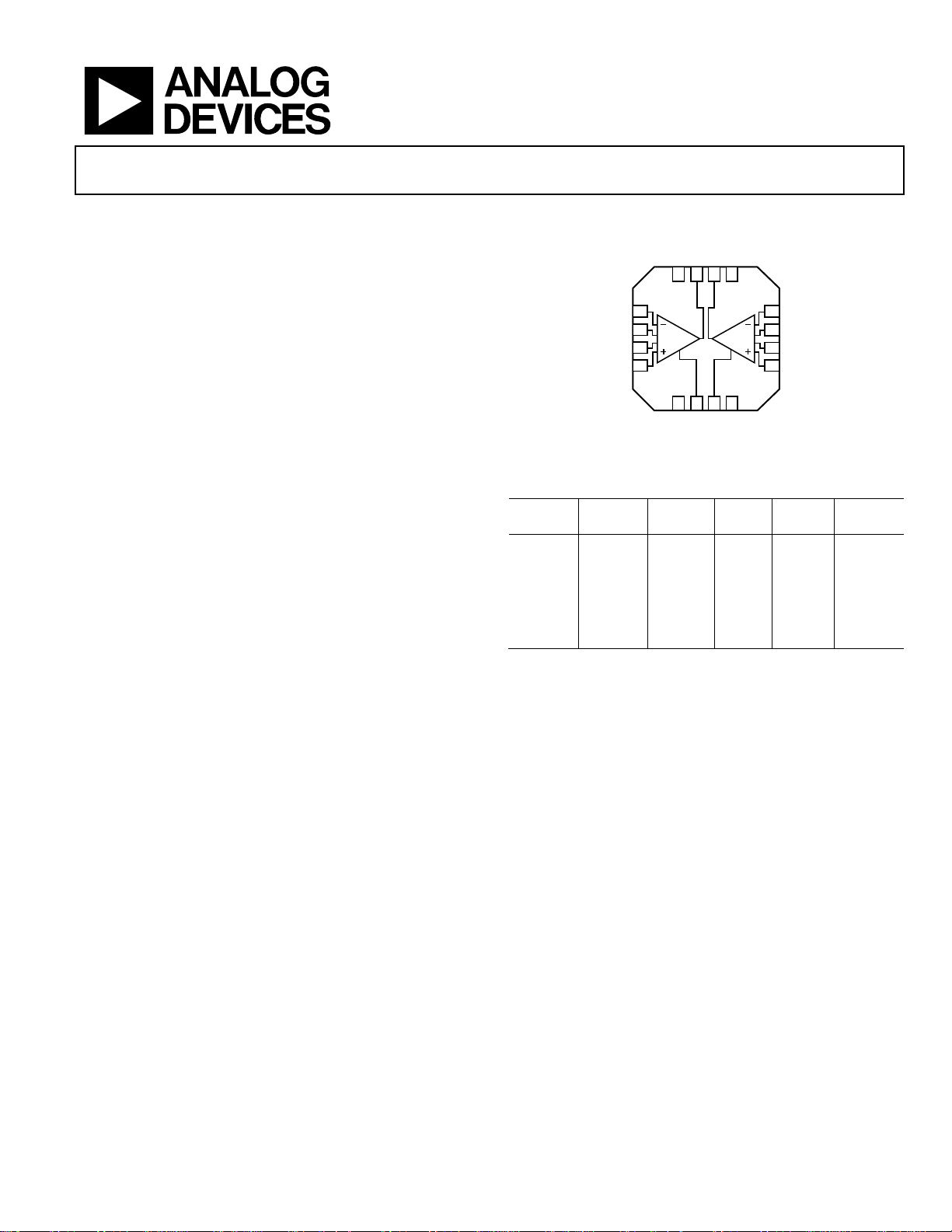
FUNCTIONAL BLOCK DIAGRAM
REF1
S
OUT2
–V
13141516
S
–V
REF2
Mil
Grade
12
11
10
9
Low
Power
–IN2
R
G2
R
G2
+IN2
06286-001
Digital
Gain
+VSOUT1
AD8224
1
–IN1
2
R
G1
3
R
G1
4
+IN1
5678
S
+V
Figure 1.
Table 1. In Amps and Difference Amplifiers by Category
High
Perform
Low
Cost
High
Voltage
AD82201 AD85531 AD628 AD620 AD6271 AD82311
AD8221 AD6231 AD629 AD621 AD8250
AD8222 AD524 AD8251
AD526 AD85551
AD624 AD85561
AD85571
1
Rail-to-rail output.
GENERAL DESCRIPTION
The AD8224 is the first single-supply, JFET input instrumentation
amplifier available in the space-saving 16-lead, 4 mm × 4 mm
LFCSP. It requires the same board area as a typical single
instrumentation amplifier yet doubles the channel density
and offers a lower cost per channel without compromising
performance.
Designed to meet the needs of high performance, portable
instrumentation, the AD8224 has a minimum common-mode
rejection ratio (CMRR) of 86 dB at dc and a minimum CMRR
of 80 dB at 10 kHz for G = 1. Maximum input bias current is
10 pA and typically remains below 300 pA over the entire
industrial temperature range. Despite the JFET inputs, the
AD8224 typically has a noise corner of only 10 Hz.
With the proliferation of mixed-signal processing, the number
of power supplies required in each system has grown. Designed
Rev. B
Information furnished by Analog Devices is believed to be accurate and reliable. However, no
responsibility is assumed by Analog Devices for its use, nor for any infringements of patents or other
rights of third parties that may result from its use. Specifications subject to change without notice. No
license is granted by implication or otherwise under any patent or patent rights of Analog Devices.
Trademarks and registered trademarks are the property of their respective owners.
to alleviate this problem, the AD8224 can operate on a ±18 V
dual supply, as well as on a single +5 V supply. The device’s railto-rail output stage maximizes dynamic range on the low
voltage supplies common in portable applications. Its ability to
run on a single 5 V supply eliminates the need for higher
voltage, dual supplies. The AD8224 draws 750 µA of quiescent
current per amplifier, making it ideal for battery powered
devices.
In addition, the AD8224 can be configured as a single-channel,
differential output, instrumentation amplifier. Differential
outputs provide high noise immunity, which can be useful when
the output signal must travel through a noisy environment, such
as with remote sensors. The configuration can also be used to
drive differential input ADCs. For a single-channel version, use
the AD8220.
One Technology Way, P.O. Box 9106, Norwood, MA 02062-9106, U.S.A.
Tel: 781.329.4700 www.analog.com
Fax: 781.461.3113 ©2007–2010 Analog Devices, Inc. All rights reserved.
Page 2

AD8224
TABLE OF CONTENTS
Features .............................................................................................. 1
Layout .......................................................................................... 21
Applications ....................................................................................... 1
Functional Block Diagram .............................................................. 1
General Description ......................................................................... 1
Revision History ............................................................................... 2
Specifications ..................................................................................... 3
Absolute Maximum Ratings ............................................................ 9
Thermal Resistance ...................................................................... 9
ESD Caution .................................................................................. 9
Pin Configuration and Function Descriptions ........................... 10
Typical Performance Characteristics ........................................... 11
Theory of Operation ...................................................................... 20
Gain Selection ............................................................................. 20
Reference Terminal .................................................................... 21
REVISION HISTORY
5/10—Rev. A to Rev. B
Changes to Features Section............................................................ 1
Added Table 10 ................................................................................. 9
Changes to Figure 3 and Table 11 ................................................. 10
Added Hidden Paddle Package Section and Exposed Paddle
Package Section and Figure 58 ...................................................... 21
Updated Outline Dimensions ....................................................... 26
Changes to Ordering Guide .......................................................... 27
4/07—Rev. 0 to Rev. A
Changes to Features, General Description, and Figure 1 ............ 1
Changes to Table 2 ............................................................................ 3
Changes to Table 3 and Table 4 ....................................................... 5
Changes to Table 5 ............................................................................ 6
Solder Wash ................................................................................. 22
Input Bias Current Return Path ............................................... 22
Input Protection ......................................................................... 22
RF Interference ........................................................................... 23
Common-Mode Input Voltage Range ..................................... 23
Applications Information .............................................................. 24
Driving an ADC ......................................................................... 24
Differential Output .................................................................... 24
Driving a Differential Input ADC ............................................ 25
Driving Cabling .......................................................................... 25
Outline Dimensions ....................................................................... 26
Ordering Guide .......................................................................... 27
Changes to Table 6 and Table 7 ....................................................... 8
Changes to Figure 2 ........................................................................... 9
Changes to Figure 3 ........................................................................ 10
Inserted Figure 4, Figure 5, and Figure 6; Renumbered
Sequentially ..................................................................................... 11
Changes to Figure 7 ........................................................................ 11
Changes to Figure 20 and Figure 21............................................. 13
Changes to Figure 28 ...................................................................... 15
Changes to Theory of Operation and Figure 55 ........................ 20
Changes to Ordering Guide .......................................................... 26
1/07—Revision 0: Initial Version
Rev. B | Page 2 of 28
Page 3

AD8224
SPECIFICATIONS
VS+ = +15 V, VS− = −15 V, V
individual instrumentation amplifier configured for a single-ended output or dual instrumentation amplifiers configured for differential
outputs as shown in Figure 63.
Table 2. Individual Amplifier in Single-Ended Configuration or Dual Amplifiers in Differential Output Configuration
A Grade B Grade
Parameter Test Conditions Min Typ Max Min Typ Max Unit
COMMON-MODE REJECTION RATIO (CMRR)
CMRR DC to 60 Hz with
1 kΩ Source Imbalance
G = 1 78 86 dB
G = 10 94 100 dB
G = 100 94 100 dB
G = 1000 94 100 dB
CMRR at 10 kHz VCM = ±10 V
G = 1 74 80 dB
G = 10 84 90 dB
G = 100 84 90 dB
G = 1000 84 90 dB
NOISE
Voltage Noise, 1 kHz
Input Voltage Noise, eni V
Output Voltage Noise, eno V
RTI, 0.1 Hz to 10 Hz
G = 1 5 5 μV p-p
G = 1000 0.8 0.8 μV p-p
Current Noise f = 1 kHz 1 1 fA/√Hz
VOLTAGE OFFSET
Input Offset, V
300 175 μV
OSI
Average TC T = −40°C to +85°C 10 5 μV/°C
Output Offset, V
1200 800 μV
OSO
Average TC T = −40°C to +85°C 10 5 μV/°C
Offset RTI vs. Supply (PSR) VS = ±5 V to ±15 V
G = 1 86 86 dB
G = 10 96 100 dB
G = 100 96 100 dB
G = 1000 96 100 dB
INPUT CURRENT (PER CHANNEL)
Input Bias Current 25 10 pA
Over Temperature3 T = −40°C to +85°C 300 300 pA
Input Offset Current 2 0.6 pA
Over Temperature3 T = −40°C to +85°C 5 5 pA
REFERENCE INPUT
RIN 40 40 kΩ
IIN V
Voltage Range −VS +VS −VS +VS V
Gain to Output
= 0 V, TA = 25°C, G = 1, RL = 2 k1, unless otherwise noted. Ta bl e 2 displays the specifications for an
REF
2
, VS = ±15 V
= ±10 V
V
CM
RTI noise =
2
√(e
+ (eno/G)2)
ni
+, VIN− = 0 V 14 14 17 nV/√Hz
IN
+, VIN− = 0 V 90 90 100 nV/√Hz
IN
=
RTI V
OS
) + (V
(V
OSI
+, VIN− = 0 V 70 70 μA
IN
OSO
/G)
1 ±
0.0001
1 ±
V/V
0.0001
Rev. B | Page 3 of 28
Page 4

AD8224
A Grade B Grade
Parameter Test Conditions Min Typ Max Min Typ Max Unit
GAIN G = 1 + (49.4 kΩ/RG)
Gain Range 1 1000 1 1000 V/V
Gain Error V
G = 1 0.06 0.04 %
G = 10 0.3 0.2 %
G = 100 0.3 0.2 %
G = 1000 0.3 0.2 %
Gain Nonlinearity V
G = 1 RL = 10 kΩ 8 15 8 15 ppm
G = 10 RL = 10 kΩ 5 10 5 10 ppm
G = 100 RL = 10 kΩ 15 25 15 25 ppm
G = 1000 RL = 10 kΩ 100 150 100 150 ppm
G = 1 RL = 2 kΩ 15 20 15 20 ppm
G = 10 RL = 2 kΩ 12 20 12 20 ppm
G = 100 RL = 2 kΩ 35 50 35 50 ppm
G=1000 RL = 2 kΩ 180 250 180 250 ppm
Gain vs. Temperature
G = 1 3 10 2 5 ppm/°C
G > 10 −50 −50 ppm/°C
INPUT
Impedance (Pin to Ground)4 104||5 104||5 GΩ||pF
Input Operating Voltage Range5
Over Temperature T = −40°C to +85°C −VS − 0.1 +VS − 2.1 −VS − 0.1 +VS − 2.1 V
OUTPUT
Output Swing RL = 2 kΩ −14.25 +14.25 −14.25 +14.25 V
Over Temperature T = −40°C to +85°C −14.3 +14.1 −14.3 +14.1 V
Output Swing RL = 10 kΩ −14.7 +14.7 −14.7 +14.7 V
Over Temperature T = −40°C to +85°C −14.6 +14.6 −14.6 +14.6 V
Short-Circuit Current 15 15 mA
POWER SUPPLY (PER AMPLIFIER)
Operating Range ±2.256 ±18 ±2.256 ±18 V
Quiescent Current 750 800 750 800 μA
Over Temperature T = −40°C to +85°C 850 900 850 900 μA
TEMPERATURE RANGE
For Specified Performance −40 +85 −40 +85 °C
Operational7 −40 +125 −40 +125 °C
1
When the output sinks more than 4 mA, use a 47 pF capacitor in parallel with the load to prevent ringing. Otherwise, use a larger load, such as 10 kΩ.
2
Refers to the differential configuration shown in . Figure 63
3
Refer to and for the relationship between input current and temperature. Figure 14 Figure 15
4
Differential and common-mode input impedance can be calculated from the pin impedance: Z
5
The AD8224 can operate up to a diode drop below the negative supply; however, the bias current increases sharply. The input voltage range reflects the maximum
allowable voltage where the input bias current is within the specification.
6
At this supply voltage, ensure that the input common-mode voltage is within the input voltage range specification.
7
The AD8224 is characterized from −40°C to +125°C. See the section for expected operation in this temperature range. Typical Performance Characteristics
= ±10 V
OUT
= −10 V to +10 V
OUT
−V
= ±2.25 V to ±18 V
V
S
− 0.1 +VS − 2 −VS − 0.1 +VS − 2 V
S
for dual supplies
= 2(Z
DIFF
); ZCM = Z
PIN
/2.
PIN
Rev. B | Page 4 of 28
Page 5

AD8224
VS+ = +15 V, VS− = −15 V, V
dynamic performance of each individual instrumentation amplifier.
= 0 V, TA = 25°C, G = 1, RL = 2 k1, unless otherwise noted. Ta bl e 3 displays the specifications for the
REF
Table 3. Dynamic Performance of Each Individual Amplifier—Single-Ended Output Configuration, V
= ±15 V
S
A Grade B Grade
Parameter Conditions Min Typ Max Min Typ Max Unit
DYNAMIC RESPONSE
Small Signal Bandwidth −3 dB
G = 1 1500 1500 kHz
G = 10 800 800 kHz
G = 100 120 120 kHz
G =1000 14 14 kHz
Settling Time 0.01% ΔVO = ±10 V step
G = 1 5 5 μs
G = 10 4.3 4.3 μs
G = 100 8.1 8.1 μs
G =1000 58 58 μs
Settling Time 0.001% ΔVO = ±10 V step
G = 1 6 6 μs
G = 10 4.6 4.6 μs
G = 100 9.6 9.6 μs
G =1000 74 74 μs
Slew Rate
G = 1 to 100 2 2 V/μs
1
When the output sinks more than 4 mA, use a 47 pF capacitor in parallel with the load to prevent ringing. Otherwise, use a larger load, such as 10 kΩ.
VS+ = +15 V, VS− = −15 V, V
= 0 V, TA = 25°C, G = 1, RL = 2 k1, unless otherwise noted. Ta bl e 4 displays the specifications for the
REF
dynamic performance of both amplifiers when used in the differential output configuration shown in Figure 63.
Table 4. Dynamic Performance of Both Amplifiers—Differential Output Configuration
2
, VS = ±15 V
A Grade B Grade
Parameter Conditions Min Typ Max Min Typ Max Unit
DYNAMIC RESPONSE
Small Signal Bandwidth −3 dB
G = 1 1500 1500 kHz
G = 10 800 800 kHz
G = 100 120 120 kHz
G =1000 14 14 kHz
Settling Time 0.01% ΔVO = ±10 V step
G = 1 5 5 μs
G = 10 4.3 4.3 μs
G = 100 8.1 8.1 μs
G =1000 58 58 μs
Settling Time 0.001% ΔVO = ±10 V step
G = 1 6 6 μs
G = 10 4.6 4.6 μs
G = 100 9.6 9.6 μs
G =1000 74 74 μs
Slew Rate
G = 1 to 100 2 2 V/μs
1
When the output sinks more than 4 mA, use a 47 pF capacitor in parallel with the load to prevent ringing. Otherwise, use a larger load, such as 10 kΩ.
2
Refers to the differential configuration shown in . Figure 63
Rev. B | Page 5 of 28
Page 6

AD8224
VS + = 5 V, VS− = 0 V, V
individual instrumentation amplifier configured for a single-ended output or dual instrumentation amplifiers configured for differential
outputs as shown in Figure 63.
Table 5. Individual Amplifier in Single-Ended Configuration or Dual Amplifiers in Differential Output Configuration
A Grade B Grade
Parameter Test Conditions Min Typ Max Min Typ Max Unit
COMMON-MODE REJECTION RATIO (CMRR)
CMRR DC to 60 Hz with
1 kΩ Source Imbalance
G = 1 78 86 dB
G = 10 94 100 dB
G = 100 94 100 dB
G = 1000 94 100 dB
CMRR at 10 kHz
G = 1 74 80 dB
G = 10 84 90 dB
G = 100 84 90 dB
G = 1000 84 90 dB
NOISE RTI noise = √(e
Voltage Noise, 1 kHz VS = ±2.5 V
Input Voltage Noise, eni V
Output Voltage Noise, eno V
RTI, 0.1 Hz to 10 Hz
G = 1 5 5 μV p-p
G = 1000 0.8 0.8 μV p-p
Current Noise f = 1 kHz 1 1 fA/√Hz
VOLTAGE OFFSET RTI VOS = (V
Input Offset, V
OSI
Average TC T = −40°C to +85°C 10 5 μV/°C
Output Offset, V
OSO
Average TC T = −40°C to +85°C 10 5 μV/°C
Offset RTI vs. Supply (PSR)
G = 1 86 86 dB
G = 10 96 100 dB
G = 100 96 100 dB
G = 1000 96 100 dB
INPUT CURRENT (PER CHANNEL)
Input Bias Current 25 10 pA
Over Temperature3 T = −40°C to +85°C 300 300 pA
Input Offset Current 2 0.6 pA
Over Temperature3 T = −40°C to +85°C 5 5 pA
REFERENCE INPUT
RIN 40 40 kΩ
IIN V
Voltage Range −VS +VS −VS +VS V
Gain to Output
= 2.5 V, TA = 25°C, G = 1, RL = 2 k1, unless otherwise noted. Ta b le 5 displays the specifications for an
REF
2
, VS =+5 V
= 0 to 2.5 V
V
CM
2
+ (eno/G)2)
ni
+, VIN− = 0 V, V
IN
+, VIN− = 0 V, V
IN
= 0 V 14 14 17 nV/√Hz
REF
= 0 V 90 90 100 nV/√Hz
REF
) + (V
OSI
/G)
OSO
300 250 μV
1200 800 μV
+, VIN− = 0 V 70 70 μA
IN
1 ±
0.0001
1 ±
0.0001
V/V
Rev. B | Page 6 of 28
Page 7

AD8224
A Grade B Grade
Parameter Test Conditions Min Typ Max Min Typ Max Unit
GAIN G = 1 + (49.4 kΩ/RG)
Gain Range 1 1000 1 1000 V/V
Gain Error
G = 1 V
G = 10 V
G = 100 V
G = 1000 V
Nonlinearity V
V
G = 1 RL = 10 kΩ 35 50 35 50 ppm
G = 10 RL = 10 kΩ 35 50 35 50 ppm
G = 100 RL = 10 kΩ 50 75 50 75 ppm
G = 1000 RL = 10 kΩ 90 115 90 115 ppm
G = 1 RL = 2 kΩ 35 50 35 50 ppm
G = 10 RL = 2 kΩ 35 50 35 50 ppm
G = 100 RL = 2 kΩ 50 75 50 75 ppm
G = 1000 RL = 2 kΩ 175 200 175 200 ppm
Gain vs. Temperature
G = 1 3 10 2 5 ppm/°C
G > 10 −50 −50 ppm/°C
INPUT
Impedance (Pin to Ground)4 104||6 104||6 GΩ||pF
Input Voltage Range5 −0.1 +VS − 2 −0.1 +VS − 2 V
Over Temperature T = −40°C to +85°C −0.1 +VS − 2.1 −0.1 +VS − 2.1 V
OUTPUT
Output Swing RL = 2 kΩ 0.25 4.75 0.25 4.75 V
Over Temperature T = −40°C to +85°C 0.3 4.70 0.3 4.70 V
Output Swing RL = 10 kΩ 0.15 4.85 0.15 4.85 V
Over Temperature T = −40°C to +85°C 0.2 4.80 0.2 4.80 V
Short-Circuit Current 15 15 mA
POWER SUPPLY (PER AMPLIFIER)
Operating Range 4.5 36 4.5 36 V
Quiescent Current 750 800 750 800 μA
Over Temperature T = −40°C to +85°C 850 900 850 900 μA
TEMPERATURE RANGE
For Specified Performance −40 +85 −40 +85 °C
Operational6 −40 +125 −40 +125 °C
1
When the output sinks more than 4 mA, use a 47 pF capacitor in parallel with the load to prevent ringing. Otherwise, use a larger load, such as 10 kΩ.
2
Refers to the differential configuration shown in . Figure 63
3
Refer to and for the relationship between input current and temperature. Figure 14 Figure 15
4
Differential and common-mode impedance can be calculated from the pin impedance: Z
5
The AD8224 can operate up to a diode drop below the negative supply, but the bias current increases sharply. The input voltage range reflects the maximum
allowable voltage where the input bias current is within the specification.
6
The AD8224 is characterized from −40°C to +125°C. See the section for expected operation in that temperature range. Typical Performance Characteristics
= 0.3 V to 2.9 V 0.06 0.04 %
OUT
= 0.3 V to 3.8 V 0.3 0.2 %
OUT
= 0.3 V to 3.8 V 0.3 0.2 %
OUT
= 0.3 V to 3.8 V 0.3 0.2 %
OUT
= 0.3 V to 2.9 V for G = 1
OUT
= 0.3 V to 3.8 V for G > 1
OUT
= 2(Z
DIFF
); ZCM = Z
PIN
/2.
PIN
Rev. B | Page 7 of 28
Page 8

AD8224
VS + = 5 V, VS− = 0 V, V
dynamic performance of each individual instrumentation amplifier.
= 2.5 V, TA = 25°C, G = 1, RL = 2 k1, unless otherwise noted. Ta b le 6 displays the specifications for the
REF
Table 6. Dynamic Performance of Each Individual Amplifier—Single-Ended Output Configuration, V
= +5 V
S
A Grade B Grade
Parameter Conditions Min Typ Max Min Typ Max Unit
DYNAMIC RESPONSE
Small Signal Bandwidth −3 dB
G = 1 1500 1500 kHz
G = 10 800 800 kHz
G = 100 120 120 kHz
G =1000 14 14 kHz
Settling Time 0.01%
G = 1 ΔVO = 3 V step 2.5 2.5 μs
G = 10 ΔVO = 4 V step 2.5 2.5 μs
G = 100 ΔVO = 4 V step 7.5 7.5 μs
G =1000 ΔVO = 4 V step 60 60 μs
Settling Time 0.001%
G = 1 ΔVO = 3 V step 3.5 3.5 μs
G = 10 ΔVO = 4 V step 3.5 3.5 μs
G = 100 ΔVO = 4 V step 8.5 8.5 μs
G =1000 ΔVO = 4 V step 75 75 μs
Slew Rate
G = 1 to 100 2 2 V/μs
1
When the output sinks more than 4 mA, use a 47 pF capacitor in parallel with the load to prevent ringing. Otherwise, use a larger load, such as 10 kΩ.
V
+ = 5 V, VS− = 0 V, V
S
= 2.5 V, TA = 25°C, G = 1, RL = 2 k1 unless otherwise noted. Ta b le 7 displays the specifications for the
REF
dynamic performance of both amplifiers when used in the differential output configuration shown in Figure 63.
Table 7. Dynamic Performance of Both Amplifiers—Differential Output Configuration
2
, VS = +5 V
A Grade B Grade
Parameter Conditions Min Typ Max Min Typ Max Unit
DYNAMIC RESPONSE
Small Signal Bandwidth −3 dB
G = 1 1500 1500 kHz
G = 10 800 800 kHz
G = 100 120 120 kHz
G =1000 14 14 kHz
Settling Time 0.01%
G = 1 ΔVO = 3 V step 2.5 2.5 μs
G = 10 ΔVO = 4 V step 2.5 2.5 μs
G = 100 ΔVO = 4 V step 7.5 7.5 μs
G =1000 ΔVO = 4 V step 60 60 μs
Settling Time 0.001%
G = 1 ΔVO = 3 V step 3.5 3.5 μs
G = 10 ΔVO = 4 V step 3.5 3.5 μs
G = 100 ΔVO = 4 V step 8.5 8.5 μs
G =1000 ΔVO = 4 V step 75 75 μs
Slew Rate
G = 1 to 100 2 2 V/μs
1
When the output sinks more than 4 mA, use a 47 pF capacitor in parallel with the load to prevent ringing. Otherwise, use a larger load, such as 10 kΩ.
2
Refers to the differential configuration shown in . Figure 63
Rev. B | Page 8 of 28
Page 9
AD8224
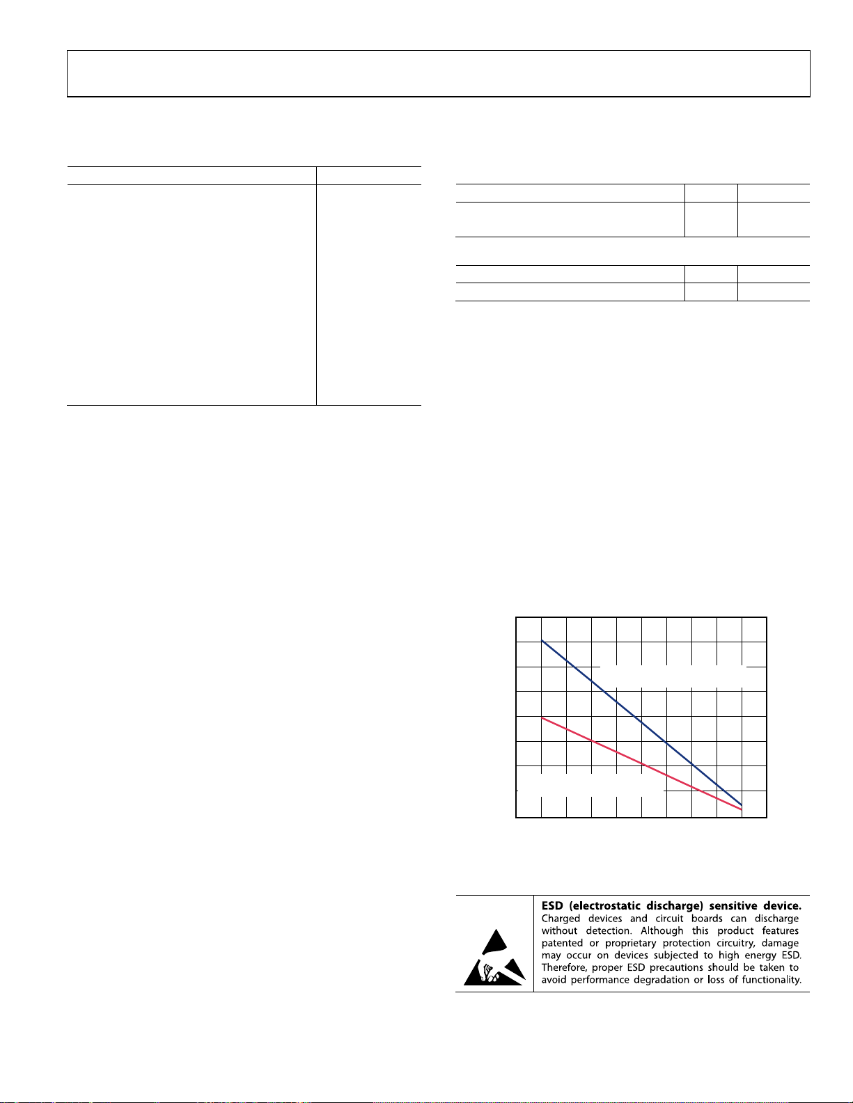
ABSOLUTE MAXIMUM RATINGS
Table 8.
Parameter Rating
Supply Voltage ±18 V
Power Dissipation See Figure 2
Output Short-Circuit Current Indefinite1
Input Voltage (Common Mode) ±VS
Differential Input Voltage ±VS
Storage Temperature Range −65°C to +130°C
Operating Temperature Range2 −40°C to +125°C
Lead Temperature (Soldering, 10 sec) 300°C
Junction Temperature 130°C
Package Glass Transition Temperature 130°C
ESD (Human Body Model) 4 kV
ESD (Charge Device Model) 1 kV
ESD (Machine Model) 0.4 kV
Stresses above those listed under Absolute Maximum Ratings
may cause permanent damage to the device. This is a stress
rating only; functional operation of the device at these or any
other conditions above those indicated in the operational
section of this specification is not implied. Exposure to absolute
maximum rating conditions for extended periods may affect
device reliability.
1
Assumes the load is referenced to midsupply.
2
Temperature for 85°C. For performance
to 125°C, see the section.
specified performance is −40°C to +
Typical Performance Characteristics
THERMAL RESISTANCE
Table 9.
Exposed Paddle Package θJA Unit
CP-16-13: LFCSP Soldered to Board 48 °C/W
CP-16-13: LFCSP Not Soldered to Board 86 °C/W
Table 10.
Hidden Paddle Package θJA Unit
CP-16-19: LFCSP 86 °C/W
The θJA values in Tabl e 9 and Tab l e 10 assume a 4-layer JEDEC
standard board. If the thermal pad is soldered to the board, it is
also assumed it is connected to a plane. θ
4.4°C/W.
Maximum Power Dissipation
The maximum safe power dissipation for the AD8224 is limited
by the associated rise in junction temperature (T
approximately 130°C, which is the glass transition temperature,
the plastic changes its properties. Even temporarily exceeding
this temperature limit may change the stresses that the package
exerts on the die, permanently shifting the parametric performance
of the amplifiers. Exceeding a temperature of 130°C for an
extended period can result in a loss of functionality. Figure 2
shows the maximum safe power dissipation in the package vs.
the ambient temperature for the LFCSP on a 4-layer JEDEC
standard board.
4.0
at the exposed pad is
JC
) on the die. At
J
3.5
3.0
2.5
2.0
1.5
1.0
= 86°C/W WHEN THERMAL PAD
JA
MAXIMUM POWER DISSIPATION (W)
IS NOT SO LDERED TO BO ARD
0.5
0
–60 –40 –20 0 20 40 60 80 100 120 140
Figure 2. Maximum Power Dissipation vs. Ambient Temperature
JA = 48°C/W WHEN THERMAL PAD
IS SOLDERED TO BOARD
AMBIENT TEM PERATURE (°C)
06286-002
ESD CAUTION
Rev. B | Page 9 of 28
Page 10

AD8224
PIN CONFIGURATION AND FUNCTION DESCRIPTIONS
S
+VSOUT1
OUT2
–V
161514
13
2
3
PIN 1
INDICAT OR
AD8224
TOP VIEW
5
S
+V
REF1 6
–IN1 1
R
G1
R
G1
+IN1 4
NOTES
1. THE AD8224 COMES IN T WO PACKAGE TYPES—EACH IS A 16 LEAD
4mm × 4mm LFCSP. O NE PACKAGE HAS AN EXPO SED THERMAL PAD,
WHICH I S CONNECTED TO +VS. THE OTHER PACKAGE TYPE DOES NOT
EXPOSE THE THERMAL PAD. SEE THE PACKAGE CONSIDERATI ONS
SECTION F OR MORE INFORMATIO N.
12
–IN2
11
R
G2
R
10
G2
+IN2
9
8
S
–V
REF2 7
06286-003
Figure 3. Pin Configuration
Table 11. Pin Function Descriptions
Pin Number Mnemonic Description
1 −IN1 Negative Input Instrumentation Amplifier (In-Amp) 1
2 RG1 Gain Resistor In-Amp 1
3 RG1 Gain Resistor In-Amp 1
4 +IN1 Positive Input In-Amp 1
5 +VS Positive Supply
6 REF1 Reference Adjust In-Amp 1
7 REF2 Reference Adjust In-Amp 2
8 −VS Negative Supply
9 +IN2 Positive Input In-Amp 2
10 RG2 Gain Resistor In-Amp 2
11 RG2 Gain Resistor In-Amp 2
12 −IN2 Negative Input In-Amp 2
13 −VS Negative Supply
14 OUT2 Output In-Amp 2
15 OUT1 Output In-Amp 1
16 +VS Positive Supply
Rev. B | Page 10 of 28
Page 11

AD8224
X
X
TYPICAL PERFORMANCE CHARACTERISTICS
25°C, VS = ±15 V, RL =10 kΩ, unless otherwise noted.
1000
400
350
300
250
200
150
NUMBER OF UNIT S
100
50
0
–40 –20 0 20 40
CMRR (µV/V)
Figure 4. Typical Distribution of CMRR (G = 1)
06286-070
100
10
VOLTAGE NOISE RTI (nV/ Hz)
1
1 100k
10 100 1k 10k
Figure 7. Voltage Spectral Density vs. Frequency
X
400
350
300
250
200
150
NUMBER OF UNIT S
100
50
0
–200 –100 0 100 200
(µV)
V
OSI
06286-071
Figure 5. Typical Distribution of Input Offset Voltage
XXX (X)
XX
XX XX
Figure 8. 0.1 Hz to 10 Hz RTI Voltage Noise (G = 1)
X
GAIN = 100 BANDWIDTH ROLL-OFF
GAIN = 1
GAIN = 10
GAIN = 100/GAIN = 1000
GAIN = 1000 BANDWIDTH ROLL-OFF
FREQUENCY (Hz)
XXX (X)
06286-009
1s/DIV5µV/DIV
06286-010
400
300
200
NUMBER OF UNITS
100
0
–1200 –900 –600 –300 0 300 600 900 1200
V
(µV)
OSO
Figure 6. Typical Distribution of Output Offset Voltage
06286-072
XXX (X)
XX
XX XX
XXX (X)
Figure 9. 0.1 Hz to 10 Hz RTI Voltage Noise (G = 1000)
1s/DIV1µV/DIV
06286-011
Rev. B | Page 11 of 28
Page 12

AD8224
4.5
4.0
3.5
3.0
(µV)
2.5
OSI
2.0
DELTA V
1.5
1.0
0.5
0
0.1 1 10 100 1000
TIME (s)
Figure 10. Change in Input Offset Voltage vs. Warmup Time
150
130
GAIN = 100
110
90
70
PSRR (dB)
50
30
GAIN = 10
GAIN = 1000
GAIN = 1
BANDWIDTH
LIMITED
INPUT OFFSET
9
CURRENT ±15
7
5
–15.1V
3
INPUT BIAS CURRENT (pA)
1
–1
–16 –12 –8 –4 0 4 8 12 16
06286-012
–5.1V
INPUT
OFFSET
CURRENT ±5
INPUT BIAS
CURRENT ±15
INPUT BIAS
CURRENT ±5
COMMON-MODE VOLTAGE (V)
0.3
0.1
–0.1
–0.3
–0.5
INPUT OFF SET CURRENT (p A)
6286-068
Figure 13. Input Bias Current and Input Offset Current vs. Common-Mode Voltage
10n
1n
100p
10p
1p
INPUT BIAS CURRE NT (A)
0.1p
I
BIAS
I
OS
10
11M
10 100 1k 10k 100k
FREQUENCY (Hz)
06286-013
Figure 11. Positive PSRR vs. Frequency, RTI
–50 150
–25 0 25 50 75 100 125
Figure 14. Input Bias Current and Offset Current vs. Temperature,
150
130
110
90
GAIN = 1
70
PSRR (dB)
50
30
10
11
GAIN = 10
GAIN = 100
10 100 1k 10k 100k
FREQUENCY (Hz)
GAIN = 1000
M
06286-014
Figure 12. Negative PSRR vs. Frequency, RTI
10n
1n
100p
10p
CURRENT (A)
1p
0.1p
–50 150
–25 0 25 50 75 100 125
Figure 15. Input Bias Current and Offset Current vs. Temperature,
TEMPERATURE (° C)
= ±15 V, V
V
S
TEMPERATURE (° C)
V
= 5 V, V
S
REF
= 0 V
REF
I
BIAS
= 2.5 V
06286-016
I
OS
06286-017
Rev. B | Page 12 of 28
Page 13

AD8224
160
140
GAIN = 1000
GAIN = 100
120
GAIN = 10
100
GAIN = 1
CMRR (dB)
80
60
40
10 100 1000 10000 100000
FREQUENCY (Hz)
BANDWIDTH
LIMITED
Figure 16. CMRR vs. Frequency
160
GAIN = 1000
140
GAIN = 100
120
GAIN = 10
GAIN = 1
100
CMRR (dB)
80
60
40
1 10 100 1000 10000 100000
FREQUENCY (Hz)
BANDWIDTH
LIMITED
Figure 17. CMRR vs. Frequency, 1 kΩ Source Imbalance
7
06286-018
06286-019
70
60
GAIN = 1000
50
40
GAIN = 100
30
20
GAIN = 10
10
GAIN (dB)
0
GAIN = 1
–10
–20
–30
–40
100 10M
1k 10k 100k 1M
FREQUENCY (Hz)
Figure 19. Gain vs. Frequency
R
LOAD
R
= 10k
XXX
NONLINEARIT Y (10ppm/DI V)
VS = ±15V
LOAD
–8–10 –6 –4 –2 0 2 4 6 8 10
OUTPUT VOLTAGE (V)
Figure 20. Gain Nonlinearity, G = 1
06286-021
= 2k
06286-022
6
5
4
3
CMRR (µV/V)
2
1
0
–50 –30 –10 10 30 50 70 90 110 130
TEMPERATURE (° C)
Figure 18. Change in CMRR vs. Temperature, G = 1
06286-020
Rev. B | Page 13 of 28
XXX
R
= 10k
LOAD
NONLINEARIT Y (10ppm/DI V)
VS = ±15V
–8–10 –6 –4 –2 0 2 4 6 8 10
OUTPUT VOLTAGE (V)
Figure 21. Gain Nonlinearity, G = 10
R
LOAD
= 2k
06286-023
Page 14

AD8224
4
+3V
+4.9V, +1.7V
+5V SINGLE SUPPLY,
V
= +2.5V
REF
+4.9V, +0.5V
–0.3V
OUTPUT VOLTAGE (V)
= 5 V, V
S
±5V SUPPLIES
OUTPUT VOLT AGE (V)
+3V
–5.3V
REF
+3V
= 2.5 V
REF
+13V
–15.3V
= 0 V
+14.9V, +5. 4V
+4.9V, +0.5V
+4.9V, –4. 1V
+14.9V, –9V
06286-027
06286-028
XXX
XXX
R
LOAD
R
= 10k
LOAD
NONLINEARIT Y (20ppm/DI V)
VS = ±15V
–8–10 –6 –4 –2 0 2 4 6 8 10
OUTPUT VOLTAGE (V)
Figure 22. Gain Nonlinearity, G = 100
R
= 2k
LOAD
R
= 10k
LOAD
NONLINEARITY (100ppm/ DIV)
VS = ±15V
–8–10 –6 –4 –2 0 2 4 6 8 10
OUTPUT VOLTAGE (V)
Figure 23. Gain Nonlinearity, G = 1000
18
12
±15V SUPPLIES
+13V
= 2k
3
2
1
0
INPUT COMMO N-MODE VOL TAGE (V)
06286-024
–1
–1 6
+0.1V, +1.7V
+0.1V, +0.5V
012345
Figure 25. Input Common-Mode Voltage Range vs. Output Voltage,
G = 1, V
18
12
6
0
–6
–12
INPUT COMMO N-MODE VOL TAGE (V)
06286-025
–18
–16 16
±15V SUPPLIES
–14.9V, +5. 4V
–4.9V, +0. 4V
–4.9V, –4.1V
–14.8V, –9V
–12 –8 –4 0 4 8 12
Figure 26. Input Common-Mode Voltage Range vs. Output Voltage,
G = 100, V
4
3
6
–14.8V, +5. 5V
0
–6
–12
INPUT COMMO N-MODE VOL TAGE (V)
–18
–16 16
–4.8V, +0. 6V
–4.8V, –3.3V
–14.8V, –8. 3V
–12 –8 –4 0 4 8 12
+3V
±5V SUPPLIES
–5.3V
–15.3V
OUTPUT VOLT AGE (V)
+14.9V, + 5.5V
+4.95V, +0.6V
+4.95V, –3. 3V
+14.9V, –8. 3V
Figure 24. Input Common-Mode Voltage Range vs. Output Voltage,
REF
= 0 V
G = 1, V
06286-026
Rev. B | Page 14 of 28
2
+0.1V, +1.7V
1
0
INPUT COMMO N-MODE VOL TAGE (V)
–1
012345
–1 6
+5V SINGLE SUPPLY,
+0.1V, –0.5V
OUTPUT VOLTAGE (V)
V
REF
–0.3V
+4.9V, +1.7V
= +2.5V
+4.9V, –0.5V
Figure 27. Input Common-Mode Voltage Range vs. Output Voltage,
G = 100, V
= 5 V, V
S
= 2.5 V
REF
06286-029
Page 15

AD8224
V
V
V
V
+
S
–1
–2
NOTES
1. THE AD8224 CAN OPE RATE UP TO A V
THE NEGATI VE SUPPLY, BUT THE BIAS CURRENT
WILL INCREASE SHARPLY.
+1
INPUT VOLTAGE LIMIT (V)
V
–
S
–1
21
+25°C–4 0°C
+85°C
4 6 8 10 12 14 16
SUPPLY VOLTAGE (V)
–40°C
+25°C
+125°C
+125°C
+85°C
Figure 28. Input Voltage Limit vs. Supply Voltage, G = 1, V
+
S
–1
–2
–3
–4
–40°C
+25°C
BELOW
BE
15
10
5
0
–5
OUTPUT VOLTAGE SWING (V)
–10
8
06286-030
=0 V
REF
+85°C
+125°C
–15
100 10k
Figure 31. Output Voltage Swing vs. Load Resistance, VS = ±15 V, V
5
–40°C
4
3
+25°C
+25°C
+125°C
–40°C
–40°C
+25°C
+125°C
+125°C
R
+85°C
LOAD
+85°C
+85°C
1k
()
REF
06286-033
= 0 V
+4
+3
OUTPUT VOLTAGE SWING (V)
+2
REFERRED TO SUPPLY VOLTAGES
+1
V
–
S
21
4 6 8 10 12 14 16
+125°C
+85°C
DUAL SUPPLY VO LTAGE (±V)
+25°C
–40°C
8
06286-031
Figure 29. Output Voltage Swing vs. Dual Supply Voltage,
R
= 2 kΩ, G = 10, V
LOAD
+
S
–0.2
+125°C
+85°C
–0.4
OUTPUT VOLTAGE SWING (V)
+0.4
REFERRED TO SUPPLY VOLTAGES
+125°C
+0.2
V
–
S
21
4 6 8 10 12 1 4 16
+25°C
+85°C
+25°C
DUAL SUPPLY VO LTAGE (±V)
–40°C
–40°C
REF
= 0 V
8
06286-032
Figure 30. Output Voltage Swing vs. Dual Supply Voltage,
= 10 kΩ, G = 10, V
R
LOAD
REF
= 0 V
2
OUTPUT VOLTAGE SWING (V)
+125°C
1
–40°C
0
100 10k
Figure 32. Output Voltage Swing vs. Load Resistance, VS = 5 V, V
+
S
–1
–2
–3
–4
+4
+3
OUTPUT VOLTAGE SWING (V)
+2
REFERRED TO SUPPLY VOLTAGES
+1
V
–
S
01
2 4 6 8 101214
Figure 33. Output Voltage Swing vs. Output Current, VS = ±15 V, V
+25°C
+85°C
1k
R
()
LOAD
+125°C +85°C
+125°C
(mA)
I
OUT
+85°C
+25°C
+25°C
06286-034
= 2.5 V
REF
–40°C
–40°C
6
06286-035
= 0 V
REF
Rev. B | Page 15 of 28
Page 16

AD8224
V
X
X
+
S
–1
+125°C
–2
+2
OUTPUT VOLTAGE SWING (V)
+1
REFERRED TO SUPPLY VOLTAGES
V
–
S
01
2 4 6 8 101214
+125°C
I
OUT
(mA)
+85°C
+85°C
+25°C
Figure 34. Output Voltage Swing vs. Output Current, VS = 5 V, V
XX
NO LOA D
XXX (X)
47pF
100pF
+25°C
35
GAIN = 10, 100, 1000
30
GAIN = 1
25
20
15
10
OUTPUT VO LTAGE SW ING (V p -p)
–40°C
6
06286-036
= 2.5 V
REF
5
0
100 10M
Figure 37. Output Voltage Swing vs. Large Signal Frequency Response
X
5V/DIV
XXX (X)
0.002%/DIV
1k 10k 100k 1M
FREQUENCY (Hz)
5µs TO 0. 01%
6µs TO 0. 001%
06286-039
XX
XX XX
5µs/DIV20mV/DIV
XXX (X)
Figure 35. Small Signal Pulse Response for Various Capacitive Loads,
= ±15 V, V
V
S
XX
NO LOAD
XXX (X)
XX
XX XX
47pF
5µs/DIV20mV/DIV
REF
100pF
XXX (X)
= 0 V
Figure 36. Small Signal Pulse Response for Various Capacitive Loads,
V
= 5 V, V
S
= 2.5 V
REF
XX
XX XX
06286-037
XXX (X)
20µs/DIV
06286-040
Figure 38. Large Signal Pulse Response and Settle Time, G = 1,
R
= 10 kΩ, VS = ±15 V, V
LOAD
X
5V/DIV
XXX (X)
0.002%/DIV
XX
XX XX
06286-038
4.3s TO 0. 01%
4.6s TO 0. 001%
XXX (X)
REF
= 0 V
20µs/DIV
06286-041
Figure 39. Large Signal Pulse Response and Settle Time, G = 10,
= 10 kΩ, VS = ±15 V, V
R
LOAD
REF
= 0 V
Rev. B | Page 16 of 28
Page 17

AD8224
XX
5V/DIV
XXX (X)
0.002%/DIV
XX
XX XX
8.1s TO 0. 01%
9.6s TO 0. 001%
XXX (X)
20µs/DIV
Figure 40. Large Signal Pulse Response and Settle Time,
G = 100, R
XX
5V/DIV
XXX (X)
0.002%/DIV
XX
XX XX
= 10 kΩ, VS = ±15 V, V
LOAD
58s TO 0.01%
74s TO 0.001 %
XXX (X)
REF
= 0 V
200µs/DIV
Figure 41. Large Signal Pulse Response and Settle Time, G = 1000,
= 10 kΩ, VS = ±15 V, V
R
LOAD
REF
= 0 V
XXX
20mV/DIV
4µs/DIV
06286-042
XXX
06286-045
Figure 43. Small Signal Pulse Response,
LOAD
20mV/DIV
= 2 kΩ, C
G = 10, R
XXX
06286-043
= 100 pF, VS = ±15 V, V
LOAD
XXX
REF
= 0 V
4µs/DIV
06286-046
Figure 44. Small Signal Pulse Response,
G = 100, R
LOAD
= 2 kΩ, C
= 100 pF, VS = ±15 V, V
LOAD
REF
= 0 V
XXX
20mV/DIV
XXX
Figure 42. Small Signal Pulse Response,
G = 1, R
LOAD
= 2 kΩ, C
= 100 pF, VS = ±15 V, V
LOAD
REF
4µs/DIV
= 0 V
06286-044
Rev. B | Page 17 of 28
XXX
G = 1000, R
20mV/DIV
XXX
Figure 45. Small Signal Pulse Response,
= 2 kΩ, C
LOAD
= 100 pF, VS = ±15 V, V
LOAD
40µs/DIV
= 0 V
REF
06286-047
Page 18

AD8224
XXX
XXX
20mV/DIV
XXX
Figure 46. Small Signal Pulse Response,
G = 1, R
20mV/DIV
LOAD
= 2 kΩ, C
= 100 pF, VS = 5 V, V
LOAD
XXX
Figure 47. Small Signal Pulse Response,
G = 10, R
LOAD
= 2 kΩ, C
= 100 pF, VS = 5 V, V
LOAD
= 2.5 V
REF
= 2.5 V
REF
4µs/DIV
4µs/DIV
XXX
20mV/DIV
40µs/DIV
06286-048
Figure 49. Small Signal Pulse Response, G = 1000, R
= 100 pF, VS = 5 V, V
C
LOAD
15
10
5
SETTLING TIME (µs)
0
02
06286-049
51015
OUTPUT VOLTAGE STEP SIZE (V)
Figure 50. Settling Time vs. Output Voltage Step Size, (G = 1) ±15 V, V
XXX
= 2.5 V
REF
SETTL ED TO 0. 001%
SETTLED TO 0.01%
LOAD
06286-051
= 2 kΩ,
0
06286-052
= 0 V
REF
100
XXX
20mV/DIV
Figure 48. Small Signal Pulse Response,
G = 100, R
LOAD
= 2 kΩ, C
= 100 pF, VS = 5 V, V
LOAD
XXX
= 2.5 V
REF
4µs/DIV
Rev. B | Page 18 of 28
SETTLED TO 0.001%
10
SETTLED TO 0.01%
SETTLING TIME (µs)
1
1 1000
06286-050
Figure 51. Settling Time vs. Gain for a 10 V Step, VS = ±15 V, V
10 100
GAIN (V/V)
REF
06286-053
= 0 V
Page 19

AD8224
R
180
SOURCE
V
= 20V p-p
OUT
160
THERMAL CROSSTALK
140
VARIES WITH LOAD
120
100
80
CHANNEL SEPARATION (dB)
60
40
1 10 100 1k 10k 100k 1M
GAIN = 1000
GAIN = 1
FREQUENCY (Hz)
SOURCE V
SMALLER TO
AVOID SLE W
RATE LIMI T
Figure 52. Channel Separation vs. Frequency,
= 2 kΩ, Source Channel at G = 1
R
LOAD
60
GAIN = 1000
40
GAIN = 100
20
GAIN = 10
GAIN (dB)
0
GAIN = 1
OUT
06286-069
100
CMR
90
80
70
LIMITED BY
MEASUREMENT
60
(dB)
OUT
CM
SYSTEM
50
40
30
20
10
0
110k1k10010 100k 1M
FREQUENCY (Hz)
OUT
= 20 log
V
DIFF_OUT
V
CM_OUT
06286-056
Figure 54. Differential Output Configuration:
Common-Mode Output (CMR
) vs. Frequency
OUT
–20
–40
10k1k100 100k 1M 10M
FREQUENCY (Hz)
Figure 53. Differential Output Configuration: Gain vs. Frequency
06286-055
Rev. B | Page 19 of 28
Page 20

AD8224
+
V
V
V
V
THEORY OF OPERATION
+
S
+V
S
IN
–V
J1
Q1
C1
V
S
PINCH
I I
+
S
NODE A
R1
24.7k
–V
S
NODE C NODE D
A1 A2
+
S
R
G
–V
S
VB
–V
NODE B
S
R2
24.7k
C2
Figure 55. Simplified Schematic
Q2
V
PINCH
+
S
20k
NODE F
20k
20k
+V
S
J2
–IN
–V
S
A3
NODE E
20k
+V
S
OUTPUT
–V
S
+V
S
REF
–V
S
06286-057
The AD8224 is a JFET input, monolithic instrumentation amplifier
based on the classic three op amp topology (see Figure 55). Input
Transistor J1 and Input Transistor J2 are biased at a fixed current so
that any input signal forces the output voltages of A1 and A2 to
change accordingly. The input signal creates a current through R
G
that flows in R1 and R2 such that the outputs of A1 and A2 provide
the correct, gained signal. Topologically, J1, A1, and R1 and J2, A2,
and R2 can be viewed as precision current feedback amplifiers with
a gain bandwidth of 1.5 MHz. The common-mode voltage and
amplified differential signal from A1 and A2 are applied to a
difference amplifier that rejects the common-mode voltage but
amplifies the differential signal. The difference amplifier employs
20 kΩ laser trimmed resistors that result in an in-amp with a gain
error of less than 0.04%. New trim techniques were developed to
ensure that the CMRR exceeds 86 dB (G = 1).
Using JFET transistors, the AD8224 offers an extremely high
input impedance, extremely low bias currents of 10 pA maximum,
low offset current of 0.6 pA maximum, and no input bias
current noise. In addition, input offset is less than 175 µV
and drift is less than 5 µV/°C. Ease of use and robustness were
considered. A common problem for instrumentation amplifiers
is that at high gains, when the input is overdriven, an excessive
milliampere input bias current can result, and the output can
undergo phase reversal.
Overdriving the input at high gains refers to when the input
signal is within the supply voltages but the amplifier cannot
output the gained signal. For example, at a gain of 100, driving
the amplifier with 10 V on ±15 V constitutes overdriving the
inputs because the amplifier cannot output 100 V.
The AD8224 has none of these problems; its input bias current
is limited to less than 10 µA, and the output does not phase
reverse under overdrive fault conditions.
The AD8224 has extremely low load induced nonlinearity. All
amplifiers that comprise the AD8224 have rail-to-rail output
capability for enhanced dynamic range. The input of the AD8224
can amplify signals with wide common-mode voltages even
slightly lower than the negative supply rail. The AD8224 operates
over a wide supply voltage range. It can operate from either a
single +4.5 V to +36 V supply or a dual ±2.25 V to ±18 V. The
transfer function of the AD8224 is
G
1 +=
k49.4
R
G
Users can easily and accurately set the gain using a single,
standard resistor. Because the input amplifiers employ a current
feedback architecture, the AD8224 gain bandwidth product
increases with gain, resulting in a system that does not experience
as much bandwidth loss as voltage feedback architectures at
higher gains.
GAIN SELECTION
Placing a resistor across the RG terminals sets the gain of the
AD8224. This is calculated by referring to Tab le 1 2 or by using
the following gain equation
k49.4
R
G
1
−=G
Rev. B | Page 20 of 28
Page 21

AD8224
(
)
Table 12. Gains Achieved Using 1% Resistors
1% Standard Table Value of RG (Ω) Calculated Gain
49.9 k 1.990
12.4 k 4.984
5.49 k 9.998
2.61 k 19.93
1.00 k 50.40
499 100.0
249 199.4
100 495.0
49.9 991.0
The AD8224 defaults to G = 1 when no gain resistor is used.
The tolerance and gain drift of the R
resistor should be added
G
to the AD8224 specifications to determine the total gain
accuracy of the system. When the gain resistor is not used,
gain error and gain drift are kept to a minimum.
REFERENCE TERMINAL
The output voltage of the AD8224 is developed with respect to
the potential on the reference terminal. This is useful when the
output signal needs to be offset to a precise midsupply level. For
example, a voltage source can be tied to the REF1 pin or the
REF2 pin to level-shift the output so that the AD8224 can drive
a single-supply ADC. Pin REFx is protected with ESD diodes
and should not exceed either +V
For best performance, source impedance to the REF terminal
should be kept below 1 Ω. As shown in Figure 55, the reference
terminal, REF, is at one end of a 20 k resistor. Additional
impedance at the REF terminal adds to this 20 k resistor and
results in amplification of the signal connected to the positive
input. The amplification from the additional R
computed by
k202
REF
RR++k40
REF
Only the positive signal path is amplified; the negative path is
unaffected. This uneven amplification degrades the CMRR of
the amplifier.
INCORRECT
AD8224
V
REF
CORRECT
V
REF
+
OP2177
–
Figure 56. Driving the Reference Pin
or −VS by more than 0.5 V.
S
can be
REF
CORRECT
AD8224
V
REF
+
AD8224
–
AD8224
06286-058
LAYOUT
The AD8224 is a high precision device. To ensure optimum
performance at the PCB level, care must be taken in the design
of the board layout. The AD8224 pinout is arranged in
a logical manner to aid in this task.
Package Considerations
The AD8224 is available in two version s of the 16-lead, 4 mm ×
4 mm LFCSP package: with or without an exposed paddle. Blindly
copying the footprint from another 4 mm × 4 mm LFCSP part
is not recommended because it may not have the same thermal
pad size and leads. Refer to the Outline Dimensions section to
verify that the PCB symbol has the correct dimensions.
Hidden Paddle Package
The AD8224 is available in an LFCSP package with a hidden
paddle. It is the preferred package for the AD8224. Unlike
chip scale packages where the pad limits routing capability,
this package allows routes and vias directly underneath the
chip, so that the full space savings of the small LFCSP can be
realized. Although the package has no metal in the center of
the part, the manufacturing process does leave a very small
section of exposed metal at each of the package corners, shown
in Figure 57 as well as Figure 68 in the Outline Dimensions
section. This metal is connected to +V
Because of a possibility of a short, vias should not be placed
underneath these exposed metal tabs.
NOTES
1. EXPOSED LEAD FRAME TABS AT THE FOUR CORNERS
OF THE PACKAG E ARE INTERNALLY CONNECTED TO
+V
. REFER TO THE OUTLINE DIMENSIONS PAGE, FOR
S
FURTHER INF ORMATION O N P ACKAGE AVAILABILITY.
Figure 57. Hidden Paddle Package: Bottom View
BOTTOM VIEW
Exposed Paddle Package
The AD8224 4 mm × 4 mm LFCSP is also available with an
exposed thermal paddle package version. This pad is connected
internally to +V
. The pad can either be left unconnected or
S
connected to the positive supply rail. Space between the leads
and thermal pad should be kept as wide as possible for the best
bias current performance. To maintain the AD8224 ultralow
bias current performance, the thermal pad area can be reduced
to extend the gap between the leads and the pad.
To preserve maximum pin compatibility with other dual
instrumentation amplifiers, such as the AD8222, leave the pad
unconnected. This can be done by not soldering the paddle at
all or by soldering the part to a landing that is a not connected
to any other net. For high vibration applications, a landing is
recommended.
through the part.
S
HIDDEN
PADDLE
EXPOSED LEAD
FRAME TABS
06286-101
Rev. B | Page 21 of 28
Page 22

AD8224
Because the AD8224 dissipates little power, heat dissipation is
rarely an issue. If improved heat dissipation is desired (for example,
when driving heavy loads), connect the exposed pad to the
positive supply rail. For the best heat dissipation performance,
the positive supply rail should be a plane in the board. See
the Thermal Resistance section for more information.
0.1µF
Common-Mode Rejection over Frequency
The AD8224 has a higher CMRR over frequency than typical
in-amps, which gives it greater immunity to disturbances, such
as line noise and its associated harmonics. A well-implemented
layout is required to maintain this high performance. Input
source impedances should be matched closely. Source resistance
should be placed close to the inputs so that it interacts with as
little parasitic capacitance as possible.
Parasitics at the R
pins can also affect CMRR over frequency.
Gx
The PCB should be laid out so that the parasitic capacitances at
each pin match. Traces from the gain setting resistor to the R
Gx
pins should be kept short to minimize parasitic inductance.
Reference
Errors introduced at the reference terminal feed directly to
the output. Take care to tie the REFx pins to the appropriate
local ground.
Power Supplies
A stable dc voltage should be used to power the instrumentation
amplifier. Noise on the supply pins can adversely affect
performance.
The AD8224 has two positive supply pins (Pin 5 and Pin 16)
and two negative supply pins (Pin 8 and Pin 13). While the part
functions with only one pin from each supply pair connected,
both pins should be connected for specified performance and
optimum reliability.
The AD8224 should be decoupled with 0.1 µF bypass capacitors,
one for each supply. Place the positive supply decoupling
capacitor near Pin 16, and the negative supply decoupling
capacitor near Pin 8. Each supply should also be decoupled with
a 10 µF tantalum capacitor. The tantalum capacitor can be
placed further away from the AD8224 and can generally be
shared by other precision integrated circuits. Figure 58 shows an
example layout.
13141516
AD8224
1
R
G
2
3
4
5678
0.1µF
Figure 58. Example Layout
12
11
10
9
R
G
SOLDER WASH
The solder process can leave flux and other contaminants on
the board. When these contaminants are between the AD8224
leads and thermal pad, they can create leakage paths that are
larger than the AD8224 bias currents. A thorough washing
process removes these contaminants and restores the device’s
excellent bias current performance.
INPUT BIAS CURRENT RETURN PATH
The input bias current of the AD8224 must have a return path
to common. When the source, such as a transformer, cannot
provide a return current path, one should be created, as shown
in Figure 59.
INPUT PROTECTION
All terminals of the AD8224 are protected against ESD. ESD
protection is guaranteed to 4 kV (human body model). In
addition, the input structure allows for dc overload conditions
a diode drop above the positive supply and a diode drop below
the negative supply. Voltages beyond a diode drop of the
supplies cause the ESD diodes to conduct and enable current to
flow through the diode. Therefore, an external resistor should
be used in series with each of the inputs to limit current for
voltages above +Vs. In either scenario, the AD8224 safely
handles a continuous 6 mA current at room temperature.
06286-059
Rev. B | Page 22 of 28
Page 23

AD8224
V
V
For applications where the AD8224 encounters extreme
overload voltages, as in cardiac defibrillators, external series
resistors and low leakage diode clamps, such as BAV199Ls,
FJH1100s, or SP720s, should be used.
INCORRECT
+V
S
AD8224
–V
S
TRANSFORME R
+V
S
C
AD8224
C
CAPACITIVELY COUPL ED
REF
–V
S
Figure 59. Creating an I
REF
f
HIGH- PASS
1
=
2RC
CAPACITIVELY COUPL ED
TRANSFORME R
C
R
C
R
Path
BIAS
CORRECT
+V
S
AD8224
–V
S
+V
S
AD8224
–V
S
REF
REF
RF INTERFERENCE
RF rectification is often a problem in applications where there are
large RF signals. The problem appears as a small dc offset voltage.
The AD8224 by its nature has a 5 pF gate capacitance (C
inputs. Matched series resistors form a natural low-pass filter that
reduces rectification at high frequency (see Figure 60).
+15
0.1µF 10µF
+IN
R
–V
R
–IN
0.1µF 10µF
C
S
C
–V
–15V
G
AD8224
G
S
+
REF
+
Figure 60. RFI Filtering Without External Capacitors
) at its
G
V
OUT
06286-061
6286-060
The relationship between external, matched series resistors and the
internal gate capacitance is expressed as
FilterFreqπ=
FilterFreqπ=
DIFF
CM
1
RC
2
G
1
RC
2
G
To eliminate high frequency common-mode signals while using
smaller source resistors, a low-pass RC network can be placed at
the input of the instrumentation amplifier (see Figure 61). The
filter limits the input signal bandwidth according to the
following relationship:
FilterFreq
FilterFreq+π=
Mismatched C
=
DIFF
CM
capacitors result in mismatched low-pass filters.
C
1
)2(2
CD
CCCR
++π
G
1
)(2
C
CCR
G
The imbalance causes the AD8224 to treat what would have
been a common-mode signal as a differential signal. To reduce
the effect of mismatched external C
greater than 10 times CC. This sets the differential filter
C
D
capacitors, select a value of
C
frequency lower than the common-mode frequency.
+15
REF
10µF
10µF
+
V
OUT
+
06286-062
R
4.02k
R
4.02k
0.1µF
C
1nF
C
+IN
C
10nF
D
C
1nF
C
AD8224
–IN
0.1µF
–15V
Figure 61. RFI Suppression
COMMON-MODE INPUT VOLTAGE RANGE
The 3-op amp architecture of the AD8224 applies gain and then
removes the common-mode voltage. Therefore, internal nodes
in the AD8224 experience a combination of both the gained
signal and the common-mode signal. This combined signal can
be limited by the voltage supplies even when the individual input
and output signals are not. Figure 24 through Figure 27 show the
allowable common-mode input voltage ranges for various
output voltages, supply voltages, and gains.
Rev. B | Page 23 of 28
Page 24

AD8224
APPLICATIONS INFORMATION
DRIVING AN ADC
An instrumentation amplifier is often used in front of an ADC
to provide CMRR and additional conditioning such as a voltage
level shift and gain (see Figure 62). In this example, a 2.7 nF
capacitor and a 500 resistor create an antialiasing filter for the
AD7685. The 2.7 nF capacitor also serves to store and deliver
the necessary charge to the switched capacitor input
of the ADC. The 500 series resistor reduces the burden
of the 2.7 nF load from the amplifier. However, large source
impedance in front of the ADC can degrade the total harmonic
distortion (THD).
For applications where THD performance is critical, the series
resistor needs to be small. At worst, a small series resistor can
load the AD8224, potentially causing the output to overshoot
or ring. In such cases, a buffer amplifier, such as the AD8615
should be used after the AD8224 to drive the ADC.
+5V
+
0.1µF10µF
+IN
REF
500
2.7nF
+2.5V
±50mV
1.07k
AD8224
–IN
Figure 62. Driving an ADC in a Low Frequency Application
AD7685
ADR435
+5V
4.7µF
DIFFERENTIAL OUTPUT
The differential configuration of the AD8224 has the same
excellent dc precision specifications as the single-ended output
configuration and is recommended for applications in the
frequency range of dc to 1 MHz.
The circuit configuration, outlined in Tab le 4 and Ta ble 7 , refers
to the configuration shown in Figure 63 only. The circuit includes
an RC filter that maintains the stability of the loop.
The transfer function for the differential output is
V
where:
G
DIFF_OUT
1 +=
= V
+OUT
k49.4
GR
− V
−OUT
= (V
+IN
− V
−IN
) × G
Setting the Common-Mode Voltage
The output common-mode voltage is set by the average of +IN2
and REF2. The transfer function is
+IN2 and REF2 have different properties that allow the
reference voltage to be easily set for a wide variety of applications.
+IN2 has high impedance but cannot swing to the positive
supply rail. REF2 must be driven with a low impedance but
can go 300 mV beyond the supply rails.
A common application sets the common-mode output voltage
to the midscale of a differential ADC. In this case, the ADC
reference voltage is sent to the +IN2 terminal, and ground is
connected to the REF2 terminal. This produces a common-
06286-063
mode output voltage of half the ADC reference voltage.
2-Channel Differential Output Using a Dual Op Amp
Another differential output topology is shown in Figure 64.
Instead of a second in-amp, ½ of a dual OP2177 op amp creates
the inverted output. Because the OP2177 comes in an MSOP,
this configuration allows the creation of a dual-channel,
precision differential output in-amp with little board area.
Errors from the op amp are common to both outputs and are,
thus, common mode. Errors from mismatched resistors also
create a common-mode dc offset. Because these errors are
common mode, they are likely to be rejected by the next
device in the signal chain.
V
CM_OUT
+IN
+
R
AD8224
G
–IN
–
AD8224
REF2
Figure 63. Differential Circuit Schematic
= (V
+IN
+OUT
+ V
−OUT
)/2 = (V
AD8224
–IN
4.99k
REF
+OUT
20k
–
33pF
+
+IN2
+ V
V
REF
REF2
+IN2
–OUT
)/2
+OUT
06286-064
+
4.99k
–
OP2177
–OUT
06286-065
Figure 64. Differential Output Using Op Amp
Rev. B | Page 24 of 28
Page 25

AD8224
V
+
0.1µF
10µF
100pF
NPO
1k
1k
0.1µF10µF
1000pF
100pF
NPO
5%
5%
+IN
–IN
+
+12
AD8224
(DIFF OUT)
+5V REF
–12V
+IN2
+OUT
–OUT
REF2
Figure 65. Driving a Differential ADC
DRIVING A DIFFERENTIAL INPUT ADC
The AD8224 can be configured in differential output mode
to drive a differential ADC. Figure 65 illustrates several of the
concepts.
First Antialiasing Filter
The 1 kΩ resistor, 1000 pF capacitor, and 100 pF capacitors in
front of the in-amp form a 76 kHz filter. This is the first of two
antialiasing filters in the circuit and helps to reduce the noise of
the system. The 100 pF capacitors protect against commonmode RFI signals. Note that they are 5% COG/NPO types.
These capacitors match well over time and temperature,
which keeps the CMRR of the system high over frequency.
Second Antialiasing Filter
An 806 Ω resistor and a 2.7 nF capacitor are located between
each AD8224 output and ADC input. These components
create a 73 kHz low-pass filter for another stage of antialiasing
protection.
These four elements also isolate the ADC from loading the
AD8224. The 806 Ω resistor shields the AD8224 from the
switched capacitor input of the ADC, which looks like a timevarying load. The 2.7 nF capacitor provides a charge to the
switched capacitor front end of the ADC. If the application
requires a lower frequency antialiasing filter, increase the value
of the capacitor rather than the resistor.
806
806
+5V
0.1µF
VDD
IN+
AD7688
IN–
+12V
V
IN
ADR435
GND
GND REF
10µF
X5R
V
OUT
0.1µF
+5V REF
06286-066
2.7nF 2.7nF
0.1µF
However, other converters have less robust inputs and may need
the added protection.
Reference
The ADR435 supplies a reference voltage to both the ADC and
the AD8224. Because REF2 on the AD8224 is grounded, the
common-mode output voltage is precisely half the reference
voltage, exactly where it needs to be for the ADC.
DRIVING CABLING
All cables have a certain capacitance per unit length, which
varies widely with cable type. The capacitive load from the cable
may cause peaking in the AD8224 output response. To reduce
peaking, use a resistor between the AD8224 and the cable.
Because cable capacitance and desired output response vary
widely, this resistor is best determined empirically. A good
starting point is 50 Ω.
The AD8224 operates at a low enough frequency that
transmission line effects are rarely an issue; therefore, the
resistor need not match the characteristic impedance of
the cable.
AD8224
(DIFF OUT)
The 806 Ω resistors can also protect an ADC from overvoltages.
Because the AD8224 runs on wider supply voltages than a
typical ADC, there is a possibility of overdriving the ADC. This
is not an issue with a PulSAR® converter, such as the AD7688.
AD8224
(SINGLE OUT)
Its input can handle a 130 mA overdrive, which is much higher
than the short-circuit limit of the AD8224.
Figure 66. Driving a Cable
06286-067
Rev. B | Page 25 of 28
Page 26
AD8224
C
A
X
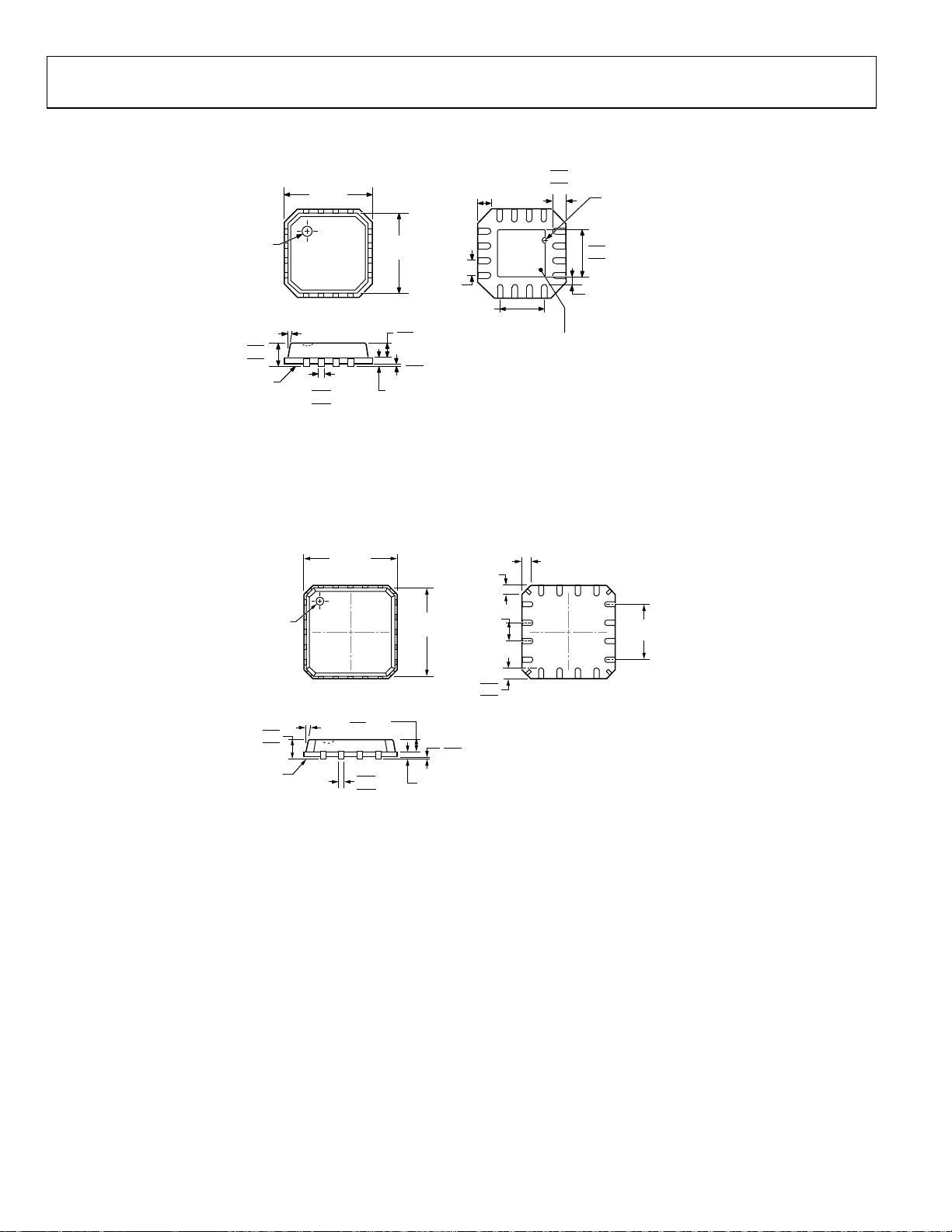
OUTLINE DIMENSIONS
PIN 1
INDI
ATO R
1.00
0.85
0.80
SEATING
PLANE
INDICATOR
SEATING
PLANE
12° MAX
4.00
BSC SQ
3.75
BSC SQ
TOP VIEW
0.80 MAX
0.65 TYP
0.05 MAX
0.30
0.23
0.18
COMPLIANTTOJEDEC STANDARDS MO-220-VGGC.
0.02 NOM
0.20 REF
0.60 MAX
12
0.65
9
BSC
1.95 BCS
COPLANARIT Y
0.08
13
EXPOSED
PA D
8
BOTTOM VIEW
Figure 67. 16-Lead Lead Frame Chip Scale Package [LFCSP_VQ]
4 mm × 4 mm Body, Very Thin Quad
(CP-16-13)
Dimensions are shown in millimeters
0.08
0.65
BSC
0.75
0.60
0.50
0.60 M
PIN 1
1.00
0.85
0.80
12° MAX
4.00
BSC SQ
TOP VIE W
0.80 MAX
0.65 TYP
0.35
0.30
0.25
3.75
BCS SQ
0.20 REF
0.60 MAX
0.05 MAX
0.02 NOM
COPLANARITY
0.50
0.40
0.30
1
16
4
5
FOR PROPER CO NNECTION O F
THE EXPOSED PAD, REFER TO
THE PIN CONF IGURATIO N AND
FUNCTION DESCRI PTIONS
SECTION O F THIS DATA SHEET.
13
12
9
8
BOTTOM VIEW
P
N
I
N
I
D
2.65
2.50 SQ
2.35
0.25 MIN
16
1
4
5
1
C
I
A
T
1.95 REF
SQ
R
O
031006-A
COMPLIANTTOJEDEC STANDARDS MO-263-VBBC
062309-B
Figure 68. 16-Lead Lead Frame Chip Scale Package [LFCSP_VQ]
4 mm × 4 mm Body, Very Thin Quad, with Hidden Paddle
CP-16-19
Dimensions shown in millimeters
Rev. B | Page 26 of 28
Page 27

AD8224
ORDERING GUIDE
Model1 Temperature Range Product Description Package Option
AD8224ACPZ-R7 −40°C to +85°C 16-Lead LFCSP_VQ CP-16-13
AD8224ACPZ-RL −40°C to +85°C 16-Lead LFCSP_VQ CP-16-13
AD8224ACPZ-WP −40°C to +85°C 16-Lead LFCSP_VQ CP-16-13
AD8224BCPZ-R7 −40°C to +85°C 16-Lead LFCSP_VQ CP-16-13
AD8224BCPZ-RL −40°C to +85°C 16-Lead LFCSP_VQ CP-16-13
AD8224BCPZ-WP −40°C to +85°C 16-Lead LFCSP_VQ CP-16-13
AD8224HACPZ-R7 −40°C to +85°C 16-Lead LFCSP_VQ CP-16-19
AD8224HACPZ-RL −40°C to +85°C 16-Lead LFCSP_VQ CP-16-19
AD8224HACPZ-WP −40°C to +85°C 16-Lead LFCSP_VQ CP-16-19
AD8224HBCPZ-R7 −40°C to +85°C 16-Lead LFCSP_VQ CP-16-19
AD8224HBCPZ-RL −40°C to +85°C 16-Lead LFCSP_VQ CP-16-19
AD8224HBCPZ-WP −40°C to +85°C 16-Lead LFCSP_VQ CP-16-19
AD8224-EVALZ Evaluation Board
1
Z = RoHS Compliant Part.
Rev. B | Page 27 of 28
Page 28

AD8224
NOTES
©2007–2010 Analog Devices, Inc. All rights reserved. Trademarks and
registered trademarks are the property of their respective owners.
D06286-0-5/10(B)
Rev. B | Page 28 of 28
 Loading...