

Page 1
Current Shunt Monitor
Data Sheet
AD8215
Rev. A
Information furnished by Analog Devices is believed to be accurate and reliable. However, no
Trademarks and registered trademarks are the property of their respective owners.
Fax: 781.461.3113 ©2008-2011 Analog Devices, Inc. All rights reserved.
07203-001
IN+
V+
OUT
G = +20
AD8215
A1
PROPRIETARY
OFFSET
CIRCUITRY
IN–
GND
FEATURES
±4000 V HBM ESD
High common-mode voltage range
−2 V to +65 V operating
−3 V to +68 V survival
Buffered output voltage
Wide operating temperature range
8-Lead SOIC_N: −40°C to +125°C
Excellent ac and dc performance
6 µV/°C typical offset drift
−8 ppm/°C typical gain drift
120 dB typical CMRR at dc
High Voltage,
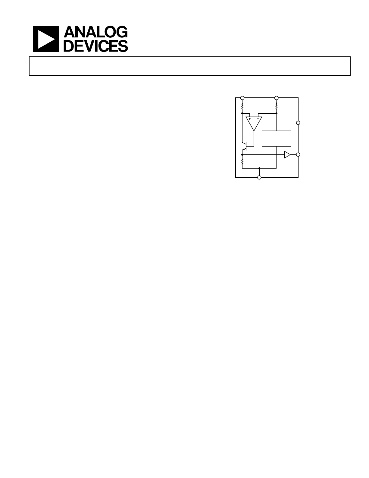
FUNCTIONAL BLOCK DIAGRAM
APPLICATIONS
High-side current sensing
Motor controls
Transmission controls
Engine management
Suspension controls
Vehicle dynamic controls
DC-to-dc converters
Qualified for automotive applications
GENERAL DESCRIPTION
The AD8215 is a high voltage, precision current shunt monitor. It
features a set gain of 20 V/V, with a maximum ±0.3% gain error
over the entire temperature range. The buffered output voltage
directly interfaces with any typical converter. Excellent commonmode rejection from −2 V to +65 V is independent of the 5 V
supply. The AD8215 performs unidirectional current
measurements across a shunt resistor in a variety of industrial
and automotive applications, such as motor controls, solenoid
controls, or battery management.
Figure 1.
Special circuitry is devoted to output linearity being maintained
throughout the input differential voltage range of 0 mV to 250 m V,
regardless of the common-mode voltage present. The AD8215
has an operating temperature range of −40°C to +125°C and is
offered in a small 8-lead SOIC_N package.
responsibility is assumed by Analog Devices for its use, nor for any infringements of patents or other
rights of third parties that may result from its use. Specifications subject to change without notice. No
license is granted by implication or otherwise under any patent or patent rights of Analog Devices.
One Technology Way, P.O. Box 9106, Norwood, MA 02062-9106, U.S.A.
Tel: 781.329.4700
www.analog.com
Page 2

AD8215 Data Sheet
TABLE OF CONTENTS
Features .............................................................................................. 1
Applications ....................................................................................... 1
Functional Block Diagram .............................................................. 1
General Description ......................................................................... 1
Revision History ............................................................................... 2
Specifications ..................................................................................... 3
Absolute Maximum Ratings ............................................................ 4
ESD Caution .................................................................................. 4
Pin Configuration and Function Descriptions ............................. 5
Typical Performance Characteristics ............................................. 6
Theory of Operation ...................................................................... 10
REVISION HISTORY
10/11—Rev. 0 to Rev. A
Change to Applications Section ...................................................... 1
Updated Outline Dimensions ....................................................... 13
Changes to Ordering Guide .......................................................... 13
Added Automotive Products Section .......................................... 13
1/08—Revision 0: Initial Version
Application Notes ........................................................................... 11
Output Linearity ......................................................................... 11
Applications Information .............................................................. 12
High-Side Current Sensing with a Low-Side Switch ............. 12
High-Side Current Sensing ....................................................... 12
Low-Side Current Sensing ........................................................ 12
Outline Dimensions ....................................................................... 13
Ordering Guide .......................................................................... 13
Automotive Products ................................................................. 13
Rev. A | Page 2 of 16
Page 3

Data Sheet AD8215
Drift
−15
+6
+18
µV/°C
T
Output Voltage Range Low
0.03 V
TA
SPECIFICATIONS
T
= −40°C to +125°C, TA = 25°C, VS = 5 V, RL = 25 kΩ (RL is the output load resistor), unless otherwise noted.
OPR
Table 1.
Parameter Min Typ Max Unit Conditions
GAIN
Initial 20 V/V
Accuracy ±0.15 % VO ≥ 0.1 V dc, TA
Accuracy Over Temperature ±0.3 % T
Drift 0 −8 −15 ppm/°C T
VOLTAGE OFFSET
Offset Voltage, RTI ±1 mV TA
Over Temperature, RTI ±2.5 mV T
INPUT
Input Impedance
Differential 5 kΩ
Common Mode 5 MΩ Common-mode voltage > 5 V
3.5 kΩ Common-mode voltage < 5 V
Common-Mode Input Voltage Range −2 +65 V Common-mode continuous
Differential Input Voltage Range 250 mV Differential input voltage
Common-Mode Rejection Ratio 100 120 dB T
80 90 dB T
OUTPUT
OPR
OPR
OPR
OPR
, f = dc to 50 kHz, VCM > 5 V
OPR
, f = dc to 40 kHz, VCM < 5 V
OPR
0.10 V T
OPR
Output Voltage Range High 4.95 V TA
4.90 V T
OPR
Output Impedance 2 Ω
DYNAMIC RESPONSE
Small Signal −3 dB Bandwidth 450 kHz T
OPR
Slew Rate 4.5 V/µs TA
NOISE
0.1 Hz to 10 Hz, RTI 7 µV p-p
Spectral Density, 1 kHz, RTI 70 nV/√Hz
POWER SUPPLY
Operating Range 4.5 5.5 V
Quiescent Current Over Temperature 1.3 2.2 mA VCM > 5 V1, T
Power Supply Rejection Ratio 75 dB T
OPR
TEMPERATURE RANGE
For Specified Performance −40 +125 °C
1
When the input common-mode voltage is less than 5 V, the supply current increases, which can be calculated by IS = −0.275 (VCM) + 2.5.
OPR
Rev. A | Page 3 of 16
Page 4
AD8215 Data Sheet
Storage Temperature Range
−65°C to +150°C
ABSOLUTE MAXIMUM RATINGS
Table 2.
Parameter Rating
Supply Voltage 12.5 V
Continuous Input Voltage −3 V to +68 V
Continuous Differential Input Voltage 0.5 V
Reverse Supply Voltage −0.3 V
Human Body Model (HBM) ESD Rating ±4000 V
Charged Device Model (CDM) ESD Rating ±1000 V
Operating Temperature Range −40°C to +125°C
Output Short-Circuit Duration Indefinite
Stresses above those listed under Absolute Maximum Ratings
may cause permanent damage to the device. This is a stress
rating only; functional operation of the device at these or any
other conditions above those indicated in the operational
section of this specification is not implied. Exposure to absolute
maximum rating conditions for extended periods may affect
device reliability.
ESD CAUTION
Rev. A | Page 4 of 16
Page 5

Data Sheet AD8215
07203-002
5
1
2
5
6
8
–IN
1
GND
2
NC
3
NC
4
+IN
8
NC
7
V+
6
OUT
5
NC = NO CONNECT
AD8215
TOP VIEW
(Not to Scale)
07203-003
6
V+
+273
−266
Supply.
PIN CONFIGURATION AND FUNCTION DESCRIPTIONS
Figure 2. Metallization Diagram
Table 3. Pin Function Descriptions
Pin No. Mnemonic X Y Description
1 −IN −228 +519 Inverting Input.
2 GND −273 −251 Ground.
3, 4, 7 NC N/A N/A No Connect.
5 OUT +265 −466 Buffered Output.
8 +IN +229 +519 Noninverting Input.
Figure 3. Pin Configuration
Rev. A | Page 5 of 16
Page 6

AD8215 Data Sheet
–1.2
–1.0
–0.8
–0.6
–0.4
–0.2
0
0.4
0.2
0.6
0.8
1.0
1.2
–40 –20 0 20
40 60 80 100 120
07203-017
TEMPERATURE (°C)
V
OSI
(mV)
07203-024
FREQUENCY ( Hz )
CMRR (dB)
60
70
80
90
100
110
120
130
140
10 100 1k 10k 100k 1M
COMMON-MODE VOLTAGE >5V
COMMON-MODE VOLTAGE <5V
–2500
–2000
–1500
–1000
–500
0
500
1000
1500
2000
2500
–40 –20 0 20 40 60 80 100 120
07203-016
TEMPERATURE (°C)
GAIN ERROR ( ppm)
–40
–35
–30
–25
–20
–15
–10
–5
0
5
10
15
20
25
30
35
40
10k 100k 1M 10M
07203-018
FREQUENCY ( Hz )
GAIN (dB)
0
1
2
3
4
5
6
7
8
9
10
0 5 10 15 20 25 30 35 40 45 50 55 60 65 70 75 80 85 90 95
DIFFERENTIAL INPUT VOLTAGE (mV)
TOTAL OUTPUT ERROR (%)
250
07203-022
–570
–560
–550
–540
–530
–520
–510
–500
–490
–480
V
IN+
V
IN–
0 25 50 75 100 125 150 175 200 225 250
07203-007
DIFFERENTIAL INPUT VOLTAGE (mV)
INPUT BIAS CURRE NT (µA)
TYPICAL PERFORMANCE CHARACTERISTICS
Figure 4. Typical Offset Drift vs. Temperature
Figure 5. Typical CMRR vs. Frequency
Figure 7. Typical Small Signal Bandwidth (V
= 200 mV p-p)
OUT
Figure 8. Total Output Error vs. Differential Input Voltage
Figure 6. Typical Gain Error vs. Temperature
Figure 9. Input Bias Current vs. Differential Input Voltage, VCM = 0 V
Rev. A | Page 6 of 16
Page 7

Data Sheet AD8215
40
50
60
70
80
90
100
110
120
0 25 50 75 100 125 150 175 200 225 250
IN+
IN–
07203-006
DIFFERENTIAL INPUT VOLTAGE (mV)
INPUT BIAS CURRE NT (µA)
–2.4
–2.0
–1.6
–1.2
–0.8
–0.4
0
0.4
0.8
–4 –2 0 2 4 6 8 65
07203-004
INPUT COMMON-MODE VOLTAGE (V)
INPUT BIAS CURRE NT (mA)
1.0
1.5
2.0
2.5
3.0
3.5
4.0
–4 –2 0 2 4 6 8 65
07203-005
INPUT COMMON-MODE VOLTAGE (V)
SUPPLY CURRENT (mA)
TIME (400ns/DIV)
07203-012
2
1
100mV/DIV
INPUT
OUTPUT
1V/DIV
TIME (400ns/DIV)
07203-015
2
1
100mV/DIV
INPUT
OUTPUT
1V/DIV
TIME (1µs/DIV)
07203-013
2
1
200mV/DIV
INPUT
OUTPUT
2V/DIV
Figure 10. Input Bias Current vs. Differential Input Voltage, VCM = 5 V
Figure 11. Input Bias Current vs. Input Common-Mode Voltage
Figure 13. Fall Time
Figure 14. Rise Time
Figure 12. Supply Current vs. Common-Mode Voltage
Figure 15. Differential Overload Recovery (Falling)
Rev. A | Page 7 of 16
Page 8

AD8215 Data Sheet
TIME (1µs/DIV)
07203-014
2
1
200mV/DIV
INPUT
OUTPUT
2V/DIV
TIME (4µs/DIV)
07203-019
2
1
2V/DIV
0.01%/DIV
TIME (4µs/DIV)
07203-020
2
1
2V/DIV
0.01%/DIV
5
6
7
8
9
10
11
12
–40 –20 0 20 40 60 80 100 120 140
07203-010
TEMPERATURE (°C)
MAXIMUM O UTPUT SINK CURRENT (mA)
4
5
6
7
8
9
10
–40 –20 0 20 40 60 80 100 120 140
07203-011
TEMPERATURE (°C)
MAXIMUM O UTPUT SOURCE CURRE NT (mA)
1.0
1.4
1.8
2.2
2.6
3.0
3.4
3.8
4.2
4.6
5.0
0 1 2 3 4 5 6 7 8 9
07203-008
OUTPUT S OURCE CURRENT (mA)
OUTPUT VOLTAGE RANGE (V)
Figure 16. Differential Overload Recovery (Rising)
Figure 17. Settling Time (Falling)
Figure 19. Maximum Output Sink Current vs. Temperature
Figure 20. Maximum Output Source Current vs. Temperature
Figure 18. Settling Time (Rising)
Figure 21. Output Voltage Range vs. Output Source Current
Rev. A | Page 8 of 16
Page 9

Data Sheet AD8215
0
0.4
0.8
1.2
1.6
2.0
0 1 2 3 4 5 6 7 8 9 10
11 12
07203-009
OUTPUT S INK CURRENT (mA)
OUTPUT VOLTAGE RANGE (V)
07203-021
VOS (mV)
COUNT
0
–2 0–1 1 2
500
1000
1500
2000
2500
3000
3500
+125°C
+25°C
–40°C
07203-023
GAIN DRIFT (ppm/°C)
COUNT
0
–2–4–6–8–10–12–14–16 0
300
600
900
1200
1500
1800
2100
2400
07203-030
OFFSET DRIFT (µV/°C)
COUNT
0
151050–5–10–15–20 20
200
400
600
800
1000
1200
1400
1600
Figure 22. Output Voltage Range from GND vs. Output Sink Current
Figure 23. Offset Distribution
Figure 24. Gain Drift Distribution
Figure 25. Offset Drift
Rev. A | Page 9 of 16
Page 10

AD8215 Data Sheet
07203-025
V+
OUT =
(I
SHUNT
× R
SHUNT
) × 20
G = +20
AD8215
A1
R1
R
OUT
I
IN
R
PROPRIETARY
OFFSET
CIRCUITRY
GND
I
SHUNT
R
SHUNT
THEORY OF OPERATION
In typical applications, the AD8215 amplifies a small differential
input voltage generated by the load current flowing through a
shunt resistor. The AD8215 rejects high common-mode voltages
(up to 65 V) and provides a ground-referenced, buffered output
that interfaces with an analog-to-digital converter (ADC). Figure
26 shows a simplified schematic of the AD8215.
A load current flowing through the external shunt resistor
produces a voltage at the input terminals of the AD8215. The
input terminals are connected to A1 by R and R1. The inverting
terminal, which has very high input impedance, is held to
(V
CM
) − (I
SHUNT
× R
SHUNT
)
because negligible current flows through R. A1 forces the
noninverting input to the same potential. Therefore, the current
that flows through R1 is equal to
I
= (I
IN
This current (I
× R
SHUNT
) is converted back to a voltage via R
IN
SHUNT
)/R1
OUT
. The
output buffer amplifier has a gain of 20 V/V and offers excellent
accuracy as the internal gain setting resistors are precision trimmed
to within 0.01% matching. The resulting output voltage is equal to
OUT = (I
SHUNT
× R
SHUNT
) × 20
Figure 26. Simplified Schematic
Rev. A | Page 10 of 16
Page 11

Data Sheet AD8215
200
0
0
07203-
026
DIFFERENTIAL INPUT VOLTAGE (mV)
OUTPUT VOLTAGE (mV)
10
180
160
140
120
100
80
60
40
20
1 2 3 4 5 6 7 8 9
IDEAL V
OUT
(mV)
V
OUT
(mV) @ VCM= 0V
V
OUT
(mV) @ VCM= 65V
APPLICATION NOTES
OUTPUT LINEARITY
In all current sensing applications, and especially in automotive
and industrial environments where the common-mode voltage
can vary significantly, it is important that the current sensor
maintain the specified output linearity, regardless of the input
differential or common-mode voltage. The AD8215 contains
specific circuitry on the input stage, which ensures that even
when the differential input voltage is very small and the
common-mode voltage is also low (below the 5 V supply), the
input-to-output linearity is maintained. Figure 27 shows the
differential input voltage vs. the corresponding output voltage at
different common modes.
Regardless of the common mode, the AD8215 provides a
correct output voltage when the differential input is at least
2 mV, which is due to the voltage range of the output amplifier
that can go as low as 33 mV typical. The specified minimum
output amplifier voltage is 100 mV to provide sufficient guardbands. The ability of the AD8215 to work with very small
differential inputs, regardless of the common-mode voltage,
allows for more dynamic range, accuracy, and flexibility in any
current sensing application.
Figure 27. Gain Linearity Due to Differential and Common-Mode Voltage
Rev. A | Page 11 of 16
Page 12

AD8215 Data Sheet
07203-027
INDUCTIVE
LOAD
CLAMP
DIODE
SHUNT
SWITCH
BATTERY
5
4
5V
8 7 6
2 3
5
1 4
NC V+IN+
IN–
OUT
NCNCGND
AD8215
07203-028
OVERCURRENT
DETECTION (<100ns)
07203-029
INDUCTIVE
LOAD
CLAMP
DIODE
SHUNT
BATTERY
SWITCH
5
4
5V
5 6 7
3 2
8
4 1
NCV+ IN+
IN–
OUT
NC NC
GND
AD8215
APPLICATIONS INFORMATION
HIGH-SIDE CURRENT SENSING WITH A LOW-SIDE SWITCH
In such load control configurations, the PWM-controlled
switch is ground referenced. An inductive load (solenoid) is tied
to a power supply. A resistive shunt is placed between the switch
and the load (see Figure 28). An advantage of placing the shunt on
the high side is that the entire current, including the recirculation
current, can be measured because the shunt remains in the loop
when the switch is off. In addition, diagnostics can be enhanced
because shorts to ground can be detected with the shunt on the
high side. In this circuit configuration, when the switch is
closed, the common-mode voltage moves down to near the
negative rail. When the switch is opened, the voltage reversal
across the inductive load causes the common-mode voltage to
be held one diode drop above the battery by the clamp diode.
GND NC –INOUT
AD8214
NC
V
REG
4
5V
5 6 7
OUT
AD8215
NC NC GND
3 2
4
4 1
+IN V
NCV+ IN+
IN–
8765
S
123
8
SHUNT
CLAMP
5
DIODE
INDUCTIVE
LOAD
SWITCH
BATTERY
HIGH-SIDE CURRENT SENSING
In this configuration, the shunt resistor is referenced to the
battery. High voltage is present at the inputs of the current sense
amplifier. In this mode, the recirculation current is again measured
and shorts to ground can be detected. When the shunt is battery
referenced, the AD8215 produces a linear ground-referenced
analog output. An AD8214 can also be used to provide an over-
current detection signal in as little as 100 ns (see Figure 29).
This feature is useful in high current systems where fast
shutdown in over-current conditions is essential.
Figure 28. Low-Side Switch
Figure 29. Battery-Referenced Shunt Resistor
LOW-SIDE CURRENT SENSING
In systems where low-side current sensing is preferred, the
AD8215 provides an integrated solution with great accuracy.
Ground noise is rejected, CMRR is typically higher than 90 dB,
and output linearity is not compromised, regardless of the input
differential voltage.
Figure 30. Ground-Referenced Shunt Resistor
Rev. A | Page 12 of 16
Page 13

Data Sheet AD8215
OUTLINE DIMENSIONS
5.00 (0.1968)
4.80 (0.1890)
4.00 (0.1574)
3.80 (0.1497)
0.25 (0.0098)
0.10 (0.0040)
COPLANARITY
0.10
SEATING
CONTROLLING DIMENSIONS ARE IN MILLIMETERS; INCH DIMENSIONS
(IN PARENTHESES) ARE ROUNDED-OFF MILLIMETER EQUIVALENTS FOR
REFERENCE ONLYAND ARE NOT APPROPRIATE FOR USE IN DESIGN.
85
1
1.27 (0.0500)
PLANE
COMPLIANT TO JEDEC STANDARDS MS-012-AA
BSC
6.20 (0.2441)
5.80 (0.2284)
4
1.75 (0.0688)
1.35 (0.0532)
0.51 (0.0201)
0.31 (0.0122)
8°
0°
0.25 (0.0098)
0.17 (0.0067)
0.50 (0.0196)
0.25 (0.0099)
1.27 (0.0500)
0.40 (0.0157)
45°
012407-A
Figure 31. 8-Lead Standard Small Outline Package [SOIC_N]
Narrow Body
(R-8)
Dimensions shown in millimeters and (inches)
ORDERING GUIDE
1, 2
Model
AD8215YRZ −40°C to +125°C 8-Lead SOIC_N R-8
AD8215YRZ-RL −40°C to +125°C 8-Lead SOIC_N, 13” Tape and Reel R-8
AD8215YRZ-R7 −40°C to +125°C 8-Lead SOIC_N, 7” Tape and Reel R-8
AD8215WYRZ −40°C to +125°C 8-Lead SOIC_N R-8
AD8215WYRZ-R7 −40°C to +125°C 8-Lead SOIC_N, 7” Tape and Reel R-8
AD8215WYRZ-RL −40°C to +125°C 8-Lead SOIC_N, 13” Tape and Reel R-8
1
Z = RoHS Compliant Part.
2
W = Qualified for Automotive Applications.
Temperature Range Package Description Package Option
AUTOMOTIVE PRODUCTS
The AD8215WYRZ models are available with controlled manufacturing to support the quality and reliability requirements of automotive
applications. Note that these automotive models may have specifications that differ from the commercial models; therefore designers
should review the Specifications section of this data sheet carefully. Only the automotive grade products shown are available for use in
automotive applications. Contact your local Analog Devices account representative for specific product ordering information and to
obtain the specific Automotive Reliability reports for these models.
Rev. A | Page 13 of 16
Page 14

AD8215 Data Sheet
NOTES
Rev. A | Page 14 of 16
Page 15

Data Sheet AD8215
NOTES
Rev. A | Page 15 of 16
Page 16

AD8215 Data Sheet
©2008-2011 Analog Devices, Inc. All rights reserved. Trademarks and
NOTES
registered trademarks are the property of their respective owners.
D07203-0-10/11(A)
Rev. A | Page 16 of 16
 Loading...