

Page 1
Precision Difference Amplifier
AD8202-KGD
Rev. 0
Trademarks and registered trademarks are the property of their respective owners.
Fax: 781.461.3113 ©2012 Analog Devices, Inc. All rights reserved.
10596-001
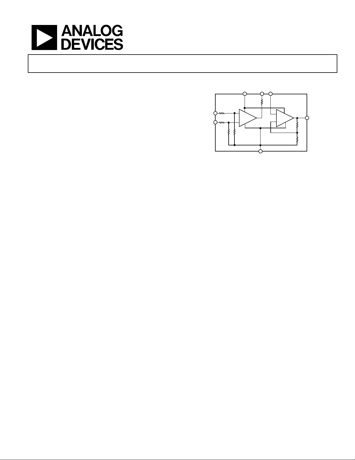
OUT
+IN
–IN
GND
+V
S
+
–
AD8202-KGD
G = 2G = 10
A1
A2
+
–
Known Good Die
FEATURES
Qualified for automotive applications
High common-mode voltage range
−8 V to +28 V operating at 5 V supply
Buffered output voltage
Gain = 20 V/V
Low-pass filter (1-pole or 2-pole)
Excellent ac and dc performance
±1 mV voltage offset
1 ppm/°C typical gain drift
80 dB CMRR minimum dc to 10 kHz
Known good die (KGD): these die are fully
guaranteed to data sheet specifications
APPLICATIONS
High-side current sensing
Motor controls
Solenoid controls
Power management
Low-side current sensing
Diagnostic protection
High Voltage,
FUNCTIONAL BLOCK DIAGRAM
Figure 1.
GENERAL DESCRIPTION
The AD8202-KGD is a single-supply difference amplifier ideal
for amplifying and low-pass filtering small differential voltages
in the presence of a large common-mode voltage. The input
common-mode voltage range extends from −8 V to +28 V at a
single +5 V supply. The AD8202-KGD is qualified for automotive
applications.
Automotive applications demand robust, precision components
for improved system control. The AD8202-KGD provides excellent
ac and dc performance, minimizing errors in the application.
Typical offset and gain drift are 5 µV/°C and 1 ppm/°C respecttively. The device also delivers a minimum CMRR of 80 dB from
dc to 10 kHz.
The AD8202-KGD features an externally accessible 100 kΩ resistor
at the output of the preamplifier (A1), which can be used for lowpass filtering and for establishing gains other than 20.
Additional application and technical information can be found
in the AD8202 data sheet.
Information furnished by Analog Devices is believed to be accurate and reliable. However, no
responsibility is assumed by Analog Devices for its use, nor for any infringements of patents or other
rights of third parties that may result from its use. Specifications subject to change without notice. No
license is granted by implication or otherwise under any patent or patent rights of Analog Devices.
One Technology Way, P.O. Box 9106, Norwood, MA 02062-9106, U.S.A.
Tel: 781.329.4700
www.analog.com
Page 2

AD8202-KGD Known Good Die
TABLE OF CONTENTS
Features .............................................................................................. 1
Applications ....................................................................................... 1
Functional Block Diagram .............................................................. 1
General Description ......................................................................... 1
Revision History ............................................................................... 2
Specifications ..................................................................................... 3
Absolute Maximum Ratings ............................................................ 4
REVISION HISTORY
3/12—Revision 0: Initial Version
ESD Caution...................................................................................4
Pad Configuration and Function Descriptions .............................5
Outline Dimensions ..........................................................................6
Die Specifications and Assembly Recommendations ..............6
Ordering Guide .............................................................................6
Automotive Products ....................................................................6
Rev. 0 | Page 2 of 8
Page 3

Known Good Die AD8202-KGD
Input Common-Mode Voltage (VCM),
−8 +28
V
PREAMPLIFIER (A1)
DYNAMIC RESPONSE
SPECIFICATIONS
T
= −40°C to +150°C, TA = 25°C, VS = 5 V.
OPR
Table 1.
Parameter Test Conditions Min Typ Max Unit
SYSTEM GAIN
Initial 20 V/V
Error 0.02 V ≤ V
vs. Temperature T
OPR
VOLTAGE OFFSET
Initial Offset (Referred to Input [RTI]) VCM = 0.15 V, TA ±1 mV
vs. Temperature T = −40°C to +125°C ±10 µV/°C
T
±15 µV/°C
OPR
INPUT
Input Impedance
Differential 260 325 390 kΩ
Common Mode 135 170 205 kΩ
Continuous
CMRR1 VCM = −8 V to +28 V
f = dc 82 dB
f = 1 kHz 82 dB
f = 10 kHz2 80 dB
≤ 4.8, dc @ TA ±0.3 %
OUT
0 +30 ppm/°C
Gain 10 V/V
Gain Error 0.02 V ≤ V
≤ (VS − 0.2 V), dc, T
OUT
±0.3 %
OPR
Output Voltage Range 0.02 4.8 V
Output Resistance 97 100 103 kΩ
OUTPUT BUFFER (A2)
Gain 2 V/V
Gain Error 0.02 V ≤ V
≤ 4.8 V dc ±0.3 %
OUT
Output Voltage Range 0.02 4.8 V
Input Bias Current 40 nA
Output Resistance 2 Ω
System Bandwidth VIN = 0.1 V p-p, V
Slew Rate VIN = 0.2 V dc, V
= 2.0 V p-p 30 50 kHz
OUT
= 4 V step 0.28 V/µs
OUT
NOISE
0.1 Hz to 10 Hz 10 µV p-p
Spectral Density, 1 kHz (RTI) 275 nV/√Hz
POWER SUPPLY
Operating Range 3.5 12 V
Quiescent Current vs. Temperature V
= 0.1 V dc
OUT
0.25 1.0 mA
PSRR VS = 3.5 V to 12 V 75 83 dB
TEMPERATURE RANGE For specified performance at T
1
Source imbalance < 2 Ω.
2
The AD8202-KGD preamplifier exceeds 80 dB CMRR at 10 kHz. However, because the output is available only by way of the 100 kΩ resistor, even a small amount of
pin-to-pin capacitance between the IN pins and the A1 and A2 pins might couple an input common-mode signal larger than the greatly attenuated preamplifier
output. The effect of pin-to-pin coupling can be negated in all applications by using a filter capacitor from Pin 3 to GND.
−40 +150 °C
OPR
Rev. 0 | Page 3 of 8
Page 4

AD8202-KGD Known Good Die
ABSOLUTE MAXIMUM RATINGS
Table 2.
Parameter Rating
Supply Voltage 12.5 V
Continuous Input Voltage (Common Mode) 35 V
Reversed Supply Voltage Protection 0.3 V
Operating Temperature Range (Die) −40°C to +150°C
Output Short-Circuit Duration Indefinite
Lead Temperature Range (Soldering, 10 sec) 300°C
Stresses above those listed under Absolute Maximum Ratings
may cause permanent damage to the device. This is a stress
rating only; functional operation of the device at these or any
other conditions above those indicated in the operational
section of this specification is not implied. Exposure to absolute
maximum rating conditions for extended periods may affect
device reliability.
ESD CAUTION
Rev. 0 | Page 4 of 8
Page 5

Known Good Die AD8202-KGD
10596-002
ADI Logo
1
2
3
4
5
6
7
8
2
−413
+285
GND
Double
Ground Pad
PAD CONFIGURATION AND FUNCTION DESCRIPTIONS
Figure 2. Pad Configuration
Table 3. Pad Function Descriptions
Coordinates
Pad No. X-Axis (µm) Y-Axis (µm) Mnemonic Pa d Typ e Description
1 −205 +409 −IN Single Inverting Input Pad
3 −413 −229 A1 Single Preamplifier (A1) Output Pad
4 −309 −410 A2 Single Buffer (A2) Input Pad
5 +272 −410 OUT Single Buffer (A2) Output Pad
6 +417 −121 +VS Single Supply Pad
7 NC No Connect
8 +205 +409 +IN Single Noninverting Input Pad
Rev. 0 | Page 5 of 8
Page 6

AD8202-KGD Known Good Die
02-22-2012-A
0.092 × 0.092
SIDE VIEW
TOP VIEW
(CIRCUIT SIDE)
1.165
1.180
0.391
0.381
0.371
1
2
3
4
5
6
7
8
Assembly Component
Recommendation
Die Attach
No special requirements
OUTLINE DIMENSIONS
Figure 3. 8-Pad Bare Die [CHIP]
(C-8-1)
Dimensions shown in millimeters
DIE SPECIFICATIONS AND ASSEMBLY RECOMMENDATIONS
Table 4. Die Specifications
Parameter Value Unit1
Chip Size 1090 × 1105 μm
Scribe Line Width 75 × 75 μm
Die Size 1.180 × 1.165 mm (maximum)
Thickness 381 ± 10 μm
Bond Pad 92 × 92 μm (minimum)
Bond Pad Composition 0.5 AlCu %
Backside Bare N/A
Passivation Polymide N/A
1
N/A means not applicable.
Table 5. Assembly Recommendations
Bonding Method Gold ball or aluminum wedge
Bonding Sequence Any
ORDERING GUIDE
Model1 Temperature Range Package Option
AD8202W-KGD-R7 −40°C to +150°C C-8-1
1
W = Qualified for Automotive Applications.
AUTOMOTIVE PRODUCTS
The AD8202W model is available with controlled manufacturing to support the quality and reliability requirements of automotive
applications. Note that this automotive model may have specifications that differ from the commercial models; therefore, designers
should review the Specifications section of this data sheet carefully. Only the automotive grade product shown is available for use in
automotive applications. Contact your local Analog Devices account representative for specific product ordering information and to
obtain the specific Automotive Reliability reports for these models.
Rev. 0 | Page 6 of 8
Page 7

Known Good Die AD8202-KGD
NOTES
Rev. 0 | Page 7 of 8
Page 8

AD8202-KGD Known Good Die
©2012 Analog Devices, Inc. All rights reserved. Trademarks and
NOTES
registered trademarks are the property of their respective owners.
D10596-0-3/12(0)
Rev. 0 | Page 8 of 8
 Loading...