

Page 1
Single Supply, Rail to Rail
1
2
3
4
8
7
6
5
TOP VIEW
(Not to Scale)
AD820
NULL
–IN
+IN
–V
S
NC
+V
S
V
OUT
NULL
1
2
3
4
8
7
6
5
TOP VIEW
(Not to Scale)
AD820
NC
–IN
+IN
–V
S
NC
+V
S
V
OUT
NC
NC = NO CONNECT
a
FEATURES
True Single Supply Operation
Output Swings Rail-to-Rail
Input Voltage Range Extends Below Ground
Single Supply Capability from +3 V to +36 V
Dual Supply Capability from ⴞ1.5 V to ⴞ18 V
Excellent Load Drive
Capacitive Load Drive Up to 350 pF
Minimum Output Current of 15 mA
Excellent AC Performance for Low Power
800 A Max Quiescent Current
Unity Gain Bandwidth: 1.8 MHz
Slew Rate of 3.0 V/s
Excellent DC Performance
800 V Max Input Offset Voltage
1 V/ⴗC Typ Offset Voltage Drift
25 pA Max Input Bias Current
Low Noise
13 nV/√Hz @ 10 kHz
APPLICATIONS
Battery Powered Precision Instrumentation
Photodiode Preamps
Active Filters
12- to 14-Bit Data Acquisition Systems
Medical Instrumentation
Low Power References and Regulators
PRODUCT DESCRIPTION
The AD820 is a precision, low power FET input op amp that
can operate from a single supply of +3.0 V to 36 V, or dual
supplies of ±1.5 V to ±18 V. It has true single supply capability
with an input voltage range extending below the negative rail,
50
45
40
35
30
25
20
NUMBER OF UNITS
15
10
5
0
1
0
INPUT BIAS CURRENT – pA
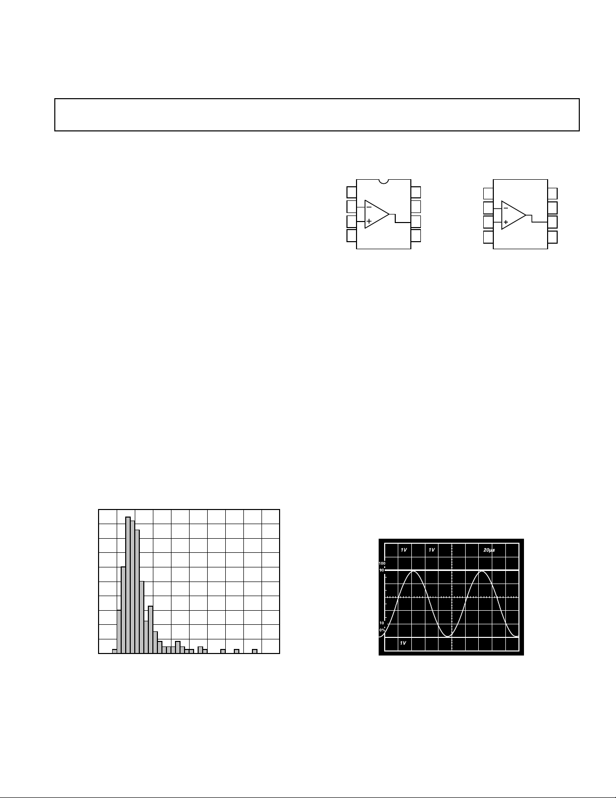
Figure 1. Typical Distribution of Input Bias Current
10
98765432
Low Power FET-Input Op Amp
AD820
CONNECTION DIAGRAMS
8-Lead Plastic Mini-DIP 8-Lead SOIC
allowing the AD820 to accommodate input signals below
ground in the single supply mode. Output voltage swing extends
to within 10 mV of each rail providing the maximum output
dynamic range.
Offset voltage of 800 µV max, offset voltage drift of 1 µV/°C, typ
input bias currents below 25 pA and low input voltage noise
provide dc precision with source impedances up to a Gigaohm.
1.8 MHz unity gain bandwidth, –93 dB THD at 10 kHz and
3 V/µs slew rate are provided for a low supply current of
800 µA. The AD820 drives up to 350 pF of direct capacitive
load and provides a minimum output current of 15 mA. This
allows the amplifier to handle a wide range of load conditions.
This combination of ac and dc performance, plus the outstanding load drive capability, results in an exceptionally versatile
amplifier for the single supply user.
The AD820 is available in three performance grades. The A and
B grades are rated over the industrial temperature range of
–40°C to +85°C. There is 3 V grade—the AD820A-3V, rated
over the industrial temperature range.
The AD820 is offered in two varieties of 8-lead package: plastic
DIP, and surface mount (SOIC).
Figure 2. Gain of +2 Amplifier; VS = +5, 0, VIN = 2.5 V Sine
Centered at 1.25 Volts
REV. B
Information furnished by Analog Devices is believed to be accurate and
reliable. However, no responsibility is assumed by Analog Devices for its
use, nor for any infringements of patents or other rights of third parties
which may result from its use. No license is granted by implication or
otherwise under any patent or patent rights of Analog Devices.
One Technology Way, P.O. Box 9106, Norwood, MA 02062-9106, U.S.A.
Tel: 781/329-4700 World Wide Web Site: http://www.analog.com
Fax: 781/326-8703 © Analog Devices, Inc., 1999
Page 2

AD820–SPECIFICATIONS
(VS = 0, 5 volts @ TA = +25ⴗC, VCM = 0 V, V
= 0.2 V unless otherwise noted)
OUT
AD820A AD820B
Parameter Conditions Min Typ Max Min Typ Max Units
DC PERFORMANCE
Initial Offset 0.1 0.8 0.1 0.4 mV
Max Offset over Temperature 0.5 1.2 0.5 0.9 mV
Offset Drift 2 2 µV/°C
Input Bias Current VO = 0 V to 4 V 2 25 2 10 pA
at T
MAX
0.5 5 0.5 2.5 nA
Input Offset Current 2 20 2 10 pA
at T
MAX
Open-Loop Gain V
T
to T
MIN
T
MIN
T
MIN
to T
to T
MAX
MAX
MAX
= 0.2 V to 4 V
O
R
= 100k 400 1000 500 1000 V/mV
L
400 400 V/mV
R
= 10k 80 150 80 150 V/mV
L
80 80 V/mV
R
= 1k 15 30 15 30 V/mV
L
10 10 V/mV
0.5 0.5 nA
NOISE/HARMONIC PERFORMANCE
Input Voltage Noise
0.1 Hz to 10 Hz 2 2 µV p-p
f = 10 Hz 25 25 nV/√Hz
f = 100 Hz 21 21 nV/√Hz
f = 1 kHz 16 16 nV/√Hz
f = 10 kHz 13 13 nV/√Hz
Input Current Noise
0.1 Hz to 10 Hz 18 18 fA p-p
f = 1 kHz 0.8 0.8 fA/√Hz
Harmonic Distortion R
= 10k to 2.5 V
L
f = 10 kHz VO = 0.25 V to 4.75 V –93 –93 dB
DYNAMIC PERFORMANCE
Unity Gain Frequency 1.8 1.8 MHz
Full Power Response V
p-p = 4.5 V 210 210 kHz
O
Slew Rate 3 3 V/µs
Settling Time
to 0.1% V
= 0.2 V to 4.5 V 1.4 1.4 µs
O
to 0.01% 1.8 1.8 µs
INPUT CHARACTERISTICS
Common-Mode Voltage Range
T
to T
MIN
CMRR V
T
MIN
Input Impedance
to T
MAX
MAX
Differential 10
Common Mode 1013储2.8 10
OUTPUT CHARACTERISTICS
Output Saturation Voltage
VOL–V
EE
T
to T
MIN
V
CC–VOH
T
MIN
V
OL–VEE
T
MIN
V
CC–VOH
T
MIN
V
OL–VEE
T
MIN
V
CC–VOH
T
MIN
to T
to T
to T
to T
to T
MAX
MAX
MAX
MAX
MAX
MAX
1
–0.2 4 –0.2 4 V
–0.2 4 –0.2 4 V
= 0 V to +2 V 66 80 72 80 dB
CM
66 66 dB
13
储0.5 10
2
I
= 20 µA 5 7 57mV
SINK
13
储0.5 Ω储pF
13
储2.8 Ω储pF
10 10 mV
I
= 20 µA 10 14 1014mV
SOURCE
20 20 mV
I
= 2 mA 40 55 40 55 mV
SINK
80 80 mV
I
= 2 mA 80 110 80 110 mV
SOURCE
160 160 mV
I
= 15 mA 300 500 300 500 mV
SINK
1000 1000 mV
I
= 15 mA 800 1500 800 1500 mV
SOURCE
1900 1900 mV
Operating Output Current 15 15 mA
T
MIN
to T
MAX
12 12 mA
Short Circuit Current 25 25 mA
Capacitive Load Drive 350 350 pF
POWER SUPPLY
Quiescent Current T
Power Supply Rejection V
T
to T
MIN
MAX
to T
MIN
S
MAX
+ = 5 V to 15 V 70 80 66 80 dB
70 66 dB
620 800 620 800 µA
REV. B–2–
Page 3

(VS = +5 volts @ TA = +25ⴗC, VCM = 0 V, V
= 0 V unless otherwise noted)
OUT
AD820
AD820A AD820B
Parameter Conditions Min Typ Max Min Typ Max Units
DC PERFORMANCE
Initial Offset 0.1 0.8 0.3 0.4 mV
Max Offset over Temperature 0.5 1.5 0.5 1 mV
Offset Drift 2 2 µV/°C
Input Bias Current VCM = –5 V to 4 V 2 25 2 10 pA
at T
MAX
0.5 5 0.5 2.5 nA
Input Offset Current 2 20 2 10 pA
at T
MAX
Open-Loop Gain V
T
to T
MIN
T
MIN
T
MIN
to T
to T
MAX
MAX
MAX
= 4 V to –4 V
O
R
= 100k 400 1000 400 1000 V/mV
L
400 400 V/mV
R
= 10k 80 150 80 150 V/mV
L
80 80 V/mV
R
= 1k 20 30 20 30 V/mV
L
10 10 V/mV
0.5 0.5 nA
NOISE/HARMONIC PERFORMANCE
Input Voltage Noise
0.1 Hz to 10 Hz 2 2 µV p-p
f = 10 Hz 25 25 nV/√Hz
f = 100 Hz 21 21 nV/√Hz
f = 1 kHz 16 16 nV/√Hz
f = 10 kHz 13 13 nV/√Hz
Input Current Noise
0.1 Hz to 10 Hz 18 18 fA p-p
f = 1 kHz 0.8 0.8 fA/√Hz
Harmonic Distortion R
f = 10 kHz V
= 10k
L
= ±4.5 V –93 –93 dB
O
DYNAMIC PERFORMANCE
Unity Gain Frequency 1.9 1.8 MHz
Full Power Response V
p-p = 9 V 105 105 kHz
O
Slew Rate 3 3 V/µs
Settling Time
to 0.1% V
= 0 V to ±4.5 V 1.4 1.4 µs
O
to 0.01% 1.8 1.8 µs
INPUT CHARACTERISTICS
Common-Mode Voltage Range
T
to T
MIN
CMRR V
T
MIN
Input Impedance
to T
MAX
MAX
Differential 10
Common Mode 1013储2.8 10
OUTPUT CHARACTERISTICS
Output Saturation Voltage
VOL–V
EE
T
to T
MIN
V
CC–VOH
T
MIN
V
OL–VEE
T
MIN
V
CC–VOH
T
MIN
V
OL–VEE
T
MIN
V
CC–VOH
T
MIN
to T
to T
to T
to T
to T
MAX
MAX
MAX
MAX
MAX
MAX
1
–5.2 4 –5.2 4 V
–5.2 4 –5.2 4 V
= –5 V to +2 V 66 80 72 80 dB
CM
66 66 dB
13
储0.5 10
2
I
= 20 µA 5 7 57mV
SINK
13
储0.5 Ω储pF
13
储2.8 Ω储pF
10 10 mV
I
= 20 µA 10 14 1014mV
SOURCE
20 20 mV
I
= 2 mA 40 55 40 55 mV
SINK
80 80 mV
I
= 2 mA 80 110 80 110 mV
SOURCE
160 160 mV
I
= 15 mA 300 500 300 500 mV
SINK
1000 1000 mV
I
= 15 mA 800 1500 800 1500 mV
SOURCE
1900 1900 mV
Operating Output Current 15 15 mA
T
MIN
to T
MAX
12 12 mA
Short Circuit Current 30 30 mA
Capacitive Load Drive 350 350 pF
POWER SUPPLY
Quiescent Current T
Power Supply Rejection V
T
to T
MIN
MAX
to T
MIN
S
MAX
+ = 5 V to 15 V 70 80 70 80 dB
70 70 dB
650 800 620 800 µA
–3–REV. B
Page 4

AD820–SPECIFICATIONS
(VS = ⴞ15 volts @ TA = +25ⴗC, VCM = 0 V, V
= 0 V unless otherwise noted)
OUT
Parameter Conditions Min Typ Max Min Typ Max Units
AD820A AD820B
DC PERFORMANCE
Initial Offset 0.4 2 0.3 1.0 mV
Max Offset over Temperature 0.5 3 0.5 2 mV
Offset Drift 2 2 µV/°C
Input Bias Current V
at T
MAX
Input Offset Current 2 20 2 10 pA
at T
MAX
Open-Loop Gain V
T
to T
MIN
T
MIN
T
MIN
to T
to T
MAX
MAX
MAX
= 0 V 2 25 2 10 pA
CM
= –10 V 40 40 pA
V
CM
VCM = 0 V 0.5 5 0.5 2.5 nA
0.5 0.5 nA
= +10 V to –10 V
O
= 100k 500 2000 500 2000 V/mV
R
L
= 10k 100 500 100 500 V/mV
R
L
= 1k 30 45 30 45 V/mV
R
L
500 500 V/mV
100 100 V/mV
20 20 V/mV
NOISE/HARMONIC PERFORMANCE
Input Voltage Noise
0.1 Hz to 10 Hz 2 2 µV p-p
f = 10 Hz 25 25 nV/√Hz
f = 100 Hz 21 21 nV/√Hz
f = 1 kHz 16 16 nV/√Hz
f = 10 kHz 13 13 nV/√Hz
Input Current Noise
0.1 Hz to 10 Hz 18 18 fA p-p
f = 1 kHz 0.8 0.8 fA/√Hz
Harmonic Distortion R
f = 10 kHz V
= 10k
L
= ±10 V –85 –85 dB
O
DYNAMIC PERFORMANCE
Unity Gain Frequency 1.9 1.9 MHz
Full Power Response V
Slew Rate 3 3 V/µs
p-p = 20 V 45 45 kHz
O
Settling Time
to 0.1% V
= 0 V to ±10 V 4.1 4.1 µs
O
to 0.01% 4.5 4.5 µs
INPUT CHARACTERISTICS
Common-Mode Voltage Range
to T
T
MIN
MAX
CMRR V
to T
T
MIN
MAX
Input Impedance
Differential 10
Common Mode 1013储2.8 10
OUTPUT CHARACTERISTICS
Output Saturation Voltage
VOL–V
EE
to T
T
MIN
MIN
MIN
MIN
MIN
MIN
to T
to T
to T
to T
to T
MAX
MAX
MAX
MAX
MAX
MAX
V
CC–VOH
T
V
OL–VEE
T
V
CC–VOH
T
V
OL–VEE
T
V
CC–VOH
T
1
–15.2 14 –15.2 14 V
–15.2 14 –15.2 14 V
= –15 V to 12 V 70 80 74 90 dB
CM
70 74 dB
13
储0.5 10
2
I
= 20 µA 5 7 57mV
SINK
13
储0.5 Ω储pF
13
储2.8 Ω储pF
10 10 mV
I
= 20 µA 10 14 1014mV
SOURCE
20 20 mV
I
= 2 mA 40 55 40 55 mV
SINK
80 80 mV
I
= 2 mA 80 110 80 110 mV
SOURCE
160 160 mV
I
= 15 mA 300 500 300 500 mV
SINK
1000 1000 mV
I
= 15 mA 800 1500 800 1500 mV
SOURCE
1900 1900 mV
Operating Output Current 20 20 mA
to T
T
MIN
MAX
15 15 mA
Short Circuit Current 45 45 mA
Capacitive Load Drive 350 350
POWER SUPPLY
Quiescent Current T
Power Supply Rejection V
T
to T
MIN
MAX
to T
MIN
S
MAX
+ = 5 V to 15 V 70 80 70 80 dB
70 70 dB
700 900 700 900 µA
–4–
REV. B
Page 5

(VS = 0, 3 volts @ TA = +25ⴗC, VCM = 0 V, V
= 0.2 V unless otherwise noted)
OUT
AD820
AD820A-3V
Parameter Conditions Min Typ Max Units
DC PERFORMANCE
Initial Offset 0.2 1 mV
Max Offset over Temperature 0.5 1.5 mV
Offset Drift 1 µV/°C
Input Bias Current V
at T
MAX
= 0 V to +2 V 2 25 pA
CM
0.5 5 nA
Input Offset Current 220 pA
at T
MAX
Open-Loop Gain V
T
to T
MIN
T
MIN
T
MIN
to T
to T
MAX
MAX
MAX
= 0.2 V to 2 V
O
R
= 100k 300 1000 V/mV
L
400 V/mV
R
= 10k 60 150 V/mV
L
80 V/mV
R
= 1k 10 30 V/mV
L
8 V/mV
0.5 nA
NOISE/HARMONIC PERFORMANCE
Input Voltage Noise
0.1 Hz to 10 Hz 2 µV p-p
f = 10 Hz 25 nV/√Hz
f = 100 Hz 21 nV/√Hz
f = 1 kHz 16 nV/√Hz
f = 10 kHz 13 nV/√Hz
Input Current Noise
0.1 Hz to 10 Hz 18 fA p-p
f = 1 kHz 0.8 fA/√Hz
Harmonic Distortion R
f = 10 kHz V
= 10k to 1.5 V
L
= ±1.25 V –92 dB
O
DYNAMIC PERFORMANCE
Unity Gain Frequency 1.5 MHz
Full Power Response V
p-p = 2.5 V 240 kHz
O
Slew Rate 3V/µs
Settling Time
to 0.1% V
= 0.2 V to 2.5 V 1 µs
O
to 0.01% 1.4 µs
INPUT CHARACTERISTICS
Common-Mode Voltage Range
T
to T
MIN
MAX
CMRR V
T
to T
MIN
MAX
Input Impedance
Differential 10
Common Mode 10
OUTPUT CHARACTERISTICS
Output Saturation Voltage
VOL–V
EE
T
to T
MIN
V
CC–VOH
T
MIN
V
OL–VEE
T
MIN
V
CC–VOH
T
MIN
V
OL–VEE
T
MIN
V
CC–VOH
T
MIN
to T
to T
to T
to T
to T
MAX
MAX
MAX
MAX
MAX
MAX
1
–0.2 2 V
–0.2 2 V
= 0 V to +1 V 60 74 dB
CM
60 dB
13
储0.5 Ω储pF
13
储2.8 Ω储pF
2
I
= 20 µA57mV
SINK
10 mV
I
= 20 µA1014mV
SOURCE
20 mV
I
= 2 mA 40 55 mV
SINK
80 mV
I
= 2 mA 80 110 mV
SOURCE
160 mV
I
= 10 mA 200 400 mV
SINK
400 mV
I
= 10 mA 500 1000 mV
SOURCE
1000 mV
Operating Output Current 15 mA
T
MIN
to T
MAX
12 mA
Short Circuit Current 18 25 mA
T
MIN
to T
MAX
15 mA
Capacitive Load Drive 350 pF
POWER SUPPLY
Quiescent Current T
Power Supply Rejection V
T
to T
MIN
MAX
to T
MIN
S
MAX
+ = 3 V to 15 V 70 80 dB
620 800 µA
70 dB
REV. B
–5–
Page 6

AD820–SPECIFICATIONS
WARNING!
ESD SENSITIVE DEVICE
NOTES
1
This is a functional specification. Amplifier bandwidth decreases when the input common-mode voltage is driven in the range (+ VS – 1 V) to +VS.
Common-mode error voltage is typically less than 5 mV with the common-mode voltage set at 1 volt below the positive supply.
2
VOL–VEE is defined as the difference between the lowest possible output voltage (VOL) and the minus voltage supply rail (VEE).
VCC–VOH is defined as the difference between the highest possible output voltage (VOH) and the positive supply voltage (VCC).
Specifications subject to change without notice.
ABSOLUTE MAXIMUM RATINGS
Supply Voltage . . . . . . . . . . . . . . . . . . . . . . . . . . . . . . . . ±18 V
Internal Power Dissipation
2
1
Plastic DIP (N) . . . . . . . . . . . . . . . . . . . . . . . . . . 1.6 Watts
SOIC (R) . . . . . . . . . . . . . . . . . . . . . . . . . . . . . . . 1.0 Watts
Input Voltage . . . . . . . . . . . . . . (+V
+ 0.2 V) to – (20 V + VS)
S
Output Short Circuit Duration . . . . . . . . . . . . . . . . Indefinite
Differential Input Voltage . . . . . . . . . . . . . . . . . . . . . . . ±30 V
Storage Temperature Range (N) . . . . . . . . . –65°C to +125°C
Storage Temperature Range (R) . . . . . . . . . –65°C to +150°C
Operating Temperature Range
AD820A/B . . . . . . . . . . . . . . . . . . . . . . . . . –40°C to +85°C
Lead Temperature Range
(Soldering 60 sec) . . . . . . . . . . . . . . . . . . . . . . . . . .+260°C
ORDERING GUIDE
Temperature Package Package
Model Range Description Options
AD820AN –40°C to +85°C 8-Lead Plastic Mini-DIP N-8
AD820BN –40°C to +85°C 8-Lead Plastic Mini-DIP N-8
AD820AR –40°C to +85°C 8-Lead SOIC R-8
AD820BR –40°C to +85°C 8-Lead SOIC R-8
AD820AR-3V –40°C to +85°C 8-Lead SOIC R-8
AD820AN-3V –40°C to +85°C 8-Lead Plastic Mini-DIP N-8
NOTES
1
Stresses above those listed under Absolute Maximum Ratings may cause perma-
nent damage to the device. This is a stress rating only; functional operation of the
device at these or any other conditions above those indicated in the operational
section of this specification is not implied. Exposure to absolute maximum rating
conditions for extended periods may affect device reliability.
2
8-Lead Plastic DIP Package: θJA = 90°C/Watt
8-Lead SOIC Package: θJA = 160°C/Watt
CAUTION
ESD (electrostatic discharge) sensitive device. Electrostatic charges as high as 4000 V readily
accumulate on the human body and test equipment and can discharge without detection.
Although the AD820 features proprietary ESD protection circuitry, permanent damage may
occur on devices subjected to high energy electrostatic discharges. Therefore, proper ESD
precautions are recommended to avoid performance degradation or loss of functionality.
REV. B–6–
Page 7

50
INPUT BIAS CURRENT – pA
5
0
–5
–5 –4 543210–1–2–3
COMMON-MODE VOLTAGE – Volts
VS = 65V
VS = 0V, +5V AND 65V
INPUT BIAS CURRENT – pA
COMMON-MODE VOLTAGE – Volts
1k
10
0.1
–16 –12 1612840–4–8
100
1
100k
100
0.1
20 40 1401201008060
1k
10k
1
10
TEMPERATURE – 8C
INPUT BIAS CURRENT – pA
40
30
20
NUMBER OF UNITS
10
Typical Characteristics–AD820
VS = 0V, 5V
0
–0.5
–0.4
OFFSET VOLTAGE – mV
0
0.5
0.40.30.20.1–0.1–0.2–0.3
Figure 3. Typical Distribution of Offset Voltage (248 Units)
48
40
32
24
% IN BIN
16
8
0
–10
–8
OFFSET VOLTAGE DRIFT – mV/8C
VS = 65V
V
= 615V
S
10
84206–2–4–6
Figure 4. Typical Distribution of Offset Voltage Drift
(120 Units)
Figure 6. Input Bias Current vs. Common-Mode
Voltage; V
= +5 V, 0 V and VS = ±5 V
S
Figure 7. Input Bias Current vs. Common-Mode
Voltage; V
= ±15 V
S
Figure 5. Typical Distribution of Input Bias Current
(213 Units)
REV. B –7–
50
45
40
35
30
25
20
NUMBER OF UNITS
15
10
5
0
1
0
INPUT BIAS CURRENT – pA
98765432
10
Figure 8. Input Bias Current vs. Temperature;
V
= 5 V, VCM = 0
S
Page 8

NEG RAIL
POS RAIL
RL = 2kV
RL = 20kV
POS
RAIL
RL = 100kV
40
–40
0 300
20
–20
60
0
180 240120
OUTPUT VOLTAGE FROM VOLTAGE RAILS – mV
INPUT VOLTAGE – mV
NEG RAIL
NEG RAIL
POS RAIL
RL = 10kV
ACL = –1
VS = 0V, 5V; V
OUT
= 4.5V p-p
VS = 0V, 3V; V
OUT
= 2.5V p-p
VS = 65V; V
OUT
= 9V p-p
–40
–90
–110
100 1k 100k10k
–60
–100
–80
–70
–50
FREQUENCY – Hz
THD – dB
VS = 615V; V
OUT
= 20V p-p
AD820–Typical Characteristics
10M
1M
100k
OPEN-LOOP GAIN –V/V
10k
100 1k 100k10k
VS = 0V, 5V
LOAD RESISTANCE – V
VS = 615V
VS = 0V, 3V
Figure 9. Open-Loop Gain vs. Load Resistance
10M
VS = 615V
VS = 0V, 5V
VS = 615V
VS = 0V, 5V
VS = 615V
VS = 0V, 5V
140
1M
100k
OPEN-LOOP GAIN – V/V
10k
–60 –40 120100806040200–20
RL = 100kV
RL = 10kV
RL = 600V
TEMPERATURE – 8C
Figure 10. Open-Loop Gain vs. Temperature
Figure 12. Input Error Voltage with Output Voltage within
300 mV of Either Supply Rail for Various Resistive Loads;
V
= ±5 V
S
1k
100
10
INPUT VOLTAGE NOISE – nV/ Hz
1
1
10 10k1k100
FREQUENCY – Hz
Figure 13. Input Voltage Noise vs. Frequency
300
200
100
RL = 10kV
0
–100
INPUT VOLTAGE – mV
–200
–300
–16
Figure 11. Input Error Voltage vs. Output Voltage for
Resistive Loads
–12
OUTPUT VOLTAGE – Volts
RL = 600V
RL = 100kV
1240–4 8–8
16
Figure 14. Total Harmonic Distortion vs. Frequency
–8–
REV. B
Page 9

AD820
100
50
0
10 100 10M1M100k10k1k
60
70
80
90
10
20
30
40
FREQUENCY – Hz
COMMON-MODE REJECTION – dB
VS = 0V, 5V
AND
V
S
= 0V, 3V
VS = 615V
POSITIVE
RAIL
+1258C
+1258C
+258C
NEGATIVE
RAIL
–55
8C
COMMON-MODE VOLTAGE FROM SUPPLY RAILS – Volts
COMMON-MODE ERROR VOLTAGE – mV
5
0
3
3
1
2
–1
4
210
–558C
VOL– V
S
1000
100
0
0.001 0.01 1001010.1
10
LOAD CURRENT – mA
OUTPUT SATURATION VOLTAGE – mV
VS – V
OH
100
80
60
40
20
OPEN-LOOP GAIN – dB
RL = 2kV
0
CL = 100pF
–20
10 100 10M1M100k10k1k
PHASE
GAIN
FREQUENCY – Hz
100
80
60
40
20
0
–20
Figure 15. Open-Loop Gain and Phase Margin vs.
Frequency
1k
ACL = +1
= 615V
V
100
S
10
PHASE MARGIN IN DEGREES
Figure 18. Common-Mode Rejection vs. Frequency
1
OUTPUT IMPEDANCE – V
0.1
0.01
100 1k 10M1M100k10k
Figure 16. Output Impedance vs. Frequency
16
12
8
4
0
–4
Figure 17. Output Swing and Error vs. Settling Time
REV. B –9–
–8
OUTPUT SWING FROM 0 TO 6Volts
–12
–16
1%
1%
1.00.0
FREQUENCY – Hz
0.01%0.1%
SETTLING TIME – ms
ERROR
Figure 19. Absolute Common-Mode Error vs. Common Mode Voltage from Supply Rails (V
4.03.02.0
5.0
– VCM)
S
Figure 20. Output Saturation Voltage vs Load Current
-
Page 10

FREQUENCY – Hz
POWER SUPPLY REJECTION – dB
120
60
0
10 100 10M1M100k10k1k
30
90
80
20
50
110
70
10
40
100
–PSRR
+PSRR
R1 = 2kV
FREQUENCY – Hz
OUTPUT VOLTAGE – Volts
30
15
0
10k 100k 10M1M
10
5
20
25
VS = 615V
VS = 0V ,3V
VS = 0V, 5V
AD820–Typical Characteristics
AD820
1000
100
10
OUTPUT SATURATION VOLTAGE – mV
1
–60 –40 140120100806040200–20
TEMPERATURE – 8C
I
SOURCE
I
SINK
I
SOURCE
I
SINK
I
SOURCE
I
SINK
= 10mA
= 10mA
= 1mA
= 1mA
= 10mA
= 10mA
Figure 21. Output Saturation Voltage vs. Temperature
80
70
60
50
40
30
20
10
SHORT CIRCUIT CURRENT LIMIT – mA
0
VS = 0V, 5V
–40–60
VS = 0V, 5V
VS = 0V, 3V
VS = 0V, 3V
TEMPERATURE – 8C
VS = 615V
VS = 615V
–OUT
120100806040200–20
+
–
–
+
+
140
Figure 22. Short Circuit Current Limit vs. Temperature
Figure 24. Power Supply Rejection vs. Frequency
Figure 25. Large Signal Frequency Response
800
700
600
500
400
300
200
QUIESCENT CURRENT – mA
100
0
40
Figure 23. Quiescent Current vs. Supply Voltage vs.
Temperature
T = +1258C
T = +258C
T = –558C
TOTAL SUPPLY VOLTAGE – Volts
3028242016128
36
–10–
REV. B
REV. B–10–
Page 11

AD820
+V
S
0.01mF
7
V
3
IN
AD820
2
6
0.01mF
4
–V
S
RL100pF
V
OUT
Figure 26. Unity-Gain Follower
Figure 27. 20 V, 25 kHz Sine Input; Unity Gain Follower;
R
= 600 Ω, VS = ±15 V
L
Figure 29. Large Signal Response Unity Gain Follower;
V
= ±15 V, RL = 10 k
S
Ω
Figure 30. Small Signal Response Unity Gain Follower;
V
= ±15 V, RL = 10 k
S
Ω
GND
Figure 28. VS = +5 V, 0 V; Unity Gain Follower Response
to 0 V to 4 V Step
REV. B –11–
GND
Figure 31. VS = +5 V, 0 V; Unity Gain Follower Response
to 0 V to 5 V Step
Page 12

AD820
GND
GND
+V
S
0.01mF
7
V
3
IN
AD820
2
6
100pF
R
4
L
V
OUT
Figure 32. Unity-Gain Follower
10kV 20kV
V
IN
Figure 33. Gain of Two Inverter
2
AD820
3
Figure 35. VS = +5 V, 0 V; Unity Gain Follower Response
to 40 mV Step Centered 40 mV Above Ground
100
GND
100pF
V
OUT
+V
S
0.01mF
7
6
R
4
L
Figure 36. VS = +5 V, 0 V; Gain of Two Inverter Response
to 20 mV Step, Centered 20 mV Below Ground
GND
Figure 34. VS = +5 V, 0 V; Gain of Two Inverter Response
to 2.5 V Step Centered –1.25 V Below Ground
Figure 37. VS = 3 V, 0 V; Gain of Two Inverter, V
25 kHz, Sine Wave Centered at –0.75 V, R
= 600
L
= 1.25 V,
IN
Ω
REV. B–12–
Page 13

AD820
AMPLIFIER-GENERATED
NOISE
RESISTOR JOHNSON
NOISE
WHENEVER JOHNSON NOISE IS GREATER THAN
AMPLIFIER NOISE, AMPLIFIER NOISE CAN BE
CONSIDERED NEGLIGIBLE FOR APPLICATION.
100k
0.1
10G
100
1
100k
10
10k
10k
1k
1G100M10M1M
SOURCE IMPEDANCE – V
INPUT VOLTAGE NOISE – mV
RMS
1kHz
10Hz
APPLICATION NOTES
INPUT CHARACTERISTICS
In the AD820, n-channel JFETs are used to provide a low offset, low noise, high impedance input stage. Minimum input
common-mode voltage extends from 0.2 V below –V
less than +V
. Driving the input voltage closer to the positive
S
to 1 V
S
rail will cause a loss of amplifier bandwidth (as can be seen by
comparing the large signal responses shown in Figures 28 and
31) and increased common-mode voltage error as illustrated in
Figure 19.
The AD820 does not exhibit phase reversal for input voltages
up to and including +V
AD820 voltage follower to a 0 V to +5 V (+V
. Figure 38a shows the response of an
S
) square wave
S
input. The input and output are superimposed. The output
polarity tracks the input polarity up to +V
—no phase reversal.
S
The reduced bandwidth above a 4 V input causes the rounding
of the output wave form. For input voltages greater than +V
, a
S
resistor in series with the AD820’s plus input will prevent phase
reversal, at the expense of greater input voltage noise. This is
illustrated in Figure 38b.
Since the input stage uses n-channel JFETs, input current during normal operation is negative; the current flows out from the
input terminals. If the input voltage is driven more positive than
+V
– 0.4 V, the input current will reverse direction as internal
S
device junctions become forward biased. This is illustrated in
Figure 6.
A current limiting resistor should be used in series with the
input of the AD820 if there is a possibility of the input voltage
exceeding the positive supply by more than 300 mV, or if an
input voltage will be applied to the AD820 when ±V
= 0. The
S
amplifier will be damaged if left in that condition for more than
10 seconds. A 1 kΩ resistor allows the amplifier to withstand up
to 10 volts of continuous overvoltage, and increases the input
voltage noise by a negligible amount.
Input voltages less than –V
are a completely different story.
S
The amplifier can safely withstand input voltages 20 volts below
the minus supply voltage as long as the total voltage from the
positive supply to the input terminal is less than 36 volts. In
addition, the input stage typically maintains picoamp level input
currents across that input voltage range.
The AD820 is designed for 13 nV/√Hz wideband input voltage
noise and maintains low noise performance to low frequencies
(refer to Figure 13). This noise performance, along with the
AD820’s low input current and current noise means that the
AD820 contributes negligible noise for applications with source
resistances greater than 10 kΩ and signal bandwidths greater
than 1 kHz. This is illustrated in Figure 39.
GND
+V
S
GND
Figure 38. (a) Response with RP = 0; VIN from 0 to +V
V
IN
Figure 36. (b) VIN = 0 to +VS + 200 mV
REV. B –13–
V
RP = 49.9 k
+5V
R
P
AD820
= 0 to +V
OUT
S
Ω
(a)
(b)
Figure 39. Total Noise vs. Source Impedance
OUTPUT CHARACTERISTICS
The AD820’s unique bipolar rail-to-rail output stage swings
within 5 mV of the minus supply and 10 mV of the positive
supply with no external resistive load. The AD820’s approxi-
mate output saturation resistance is 40 Ω sourcing and 20 Ω
sinking. This can be used to estimate output saturation voltage
when driving heavier current loads. For instance, when sourcing
5 mA, the saturation voltage to the positive supply rail will be
200 mV, when sinking 5 mA, the saturation voltage to the
minus rail will he 100 mV.
The amplifier’s open-loop gain characteristic will change as a
function of resistive load, as shown in Figures 9 through 12. For
load resistances over 20 kΩ, the AD820’s input error voltage is
V
OUT
virtually unchanged until the output voltage is driven to 180 mV
of either supply.
If the AD820’s output is driven hard against the output satura-
S
tion voltage, it will recover within 2 µs of the input returning to
the amplifier’s linear operating region.
Page 14

AD820
100V
20kV
AD820
V
OUT
0.01mF
+V
S
V
IN
0.01mF
–V
S
3
2
4
7
6
20pF
Direct capacitive load will interact with the amplifier’s effective
output impedance to form an additional pole in the amplifier’s
feedback loop, which can cause excessive peaking on the pulse
response or loss of stability. Worst case is when the amplifier is
used as a unity gain follower. Figure 40 shows the AD820’s
pulse response as a unity gain follower driving 350 pF. This
amount of overshoot indicates approximately 20 degrees of
phase margin—the system is stable, but is nearing the edge.
Configurations with less loop gain, and as a result less loop
bandwidth, will be much less sensitive to capacitance load effects. Figure 41 is a plot of capacitive load that will result in a
20 degree phase margin versus noise gain for the AD820. Noise
gain is the inverse of the feedback attenuation factor provided
by the feedback network in use.
Figure 40. Small Signal Response of AD820 as Unity Gain
Follower Driving 350 pF Capacitive Load
5
Figure 42. Extending Unity Gain Follower Capacitive Load
Capability Beyond 350 pF
OFFSET VOLTAGE ADJUSTMENT
The AD820’s offset voltage is low, so external offset voltage
nulling is not usually required. Figure 43 shows the recommended technique for AD820’s packaged in plastic DIPs.
Adjusting offset voltage in this manner will change the offset
voltage temperature drift by 4 µV/°C for every millivolt of in-
duced offset. The null pins are not functional for AD820s in the
SO-8 “R” package.
+V
S
7
3
S
5
6
1
20kV
AD820
2
4
–V
Figure 43. Offset Null
4
I
F
R
R
Single Supply Half-Wave and Full-Wave Rectifiers
An AD820 configured as a unity gain follower and operated
with a single supply can be used as a simple half-wave rectifier.
APPLICATIONS
3
The AD820’s inputs maintain picoamp level input currents even
when driven well below the minus supply. The rectifier puts that
NOISE GAIN – 1+
2
behavior to good use, maintaining an input impedance of over
11
Ω for input voltages from 1 volt from the positive supply to
10
20 volts below the negative supply.
The full and half-wave rectifier shown in Figure 44 operates as
1
300
1k 3k 10k 30k
CAPACITIVE LOAD FOR 208 PHASE MARGIN – pF
follows: when V
the unity gain follower A1 and the loop of amplifier A2. This
forces the inputs of A2 to be equal, thus no current flows through
R1 or R2, and the circuit output tracks the input. When V
is above ground, R1 is bootstrapped through
IN
is
IN
below ground, the output of A1 is forced to ground. The non-
R
F
R
I
inverting input of amplifier A2 sees the ground level output of
A1, therefore A2 operates as a unity gain inverter. The output at
node C is then a full-wave rectified version of the input. Node B
is a buffered half-wave rectified version of the input. Input volt-
Figure 41. Capacitive Load Tolerance vs. Noise Gain
ages up to ±18 volts can be rectified, depending on the voltage
supply used.
Figure 42 shows a possible configuration for extending capacitance load drive capability for a unity gain follower. With these
component values, the circuit will drive 5,000 pF with a 10%
overshoot.
REV. B–14–
Page 15

AD820
FREQUENCY – Hz
0.1
FILTER GAIN RESPONSE – dB
0
–10
–100
–20
–30
–40
–50
–60
–70
–80
–90
1 10 100 1k
C2
0.022mF
V
OUT
0.01mF
+V
S
V
IN
0.01mF
–V
S
3
2
4
7
6
AD820
R1
243kV
C3
0.022mF
C1
0.022mF
R2
243kVR3243kV
R1
100kV
+V
S
A
V
IN
0.01mF
7
3
2
A1
AD820
4
6
R2
100kV
+V
S
0.01mF
7
3
2
A2
AD820
4
6
C
FULL-WAVE
RECTIFIED OUTPUT
B
HALF-WAVE
RECTIFIED OUTPUT
A
B
C
Figure 44. Single Supply Half- and Full-Wave Rectifier
Low Power Three-Pole Sallen Key Low-Pass Filter
The AD820’s high input impedance makes it a good selection
for active filters. High value resistors can be used to construct
low frequency filters with capacitors much less than 1 µF. The
AD820’s picoamp level input currents contribute minimal dc
errors.
Figure 46 shows an example, a 10 Hz three-pole Sallen Key
Filter. The high value used for R1 minimizes interaction with
signal source resistance. Pole placement in this version of the
filter minimizes the Q associated with the two-pole section of
the filter. This eliminates any peaking of the noise contribution
of resistors R1, R2, and R3, thus minimizing the inherent output voltage noise of the filter.
4.5 Volt Low Dropout, Low Power Reference
The rail-to-rail performance of the AD820 can be used to provide low dropout performance for low power reference circuits
powered with a single low voltage supply. Figure 45 shows a
4.5 volt reference using the AD820 and the AD680, a low power
2.5 volt bandgap reference. R2 and R3 set up the required gain
of 1.8 to develop the 4.5 volt output. R1 and C2 form a lowpass RC filter to reduce the noise contribution of the AD680.
Figure 45. Single Supply 4.5 Volt Low Dropout Reference
With a 1 mA load, this reference maintains the 4.5 volt output
with a supply voltage down to 4.7 volts. The amplitude of the
recovery transient for a 1 mA to 10 mA step change in load
current is under 20 mV, and settles out in a few microseconds.
Output voltage noise is less than 10 µV rms in a 25 kHz noise
bandwidth.
REV. B –15–
R1
100kV
U2
AD820
+5V
2
3
U1
+2.5V 610mV
6
AD680
4
C1
0.1mF
6
7
3
C2
0.1mF FILM
+2.5V
OUTPUT
+4.5V
OUTPUT
R2
80kV
4
(20kV)
2
R3
100kV
(25kV)
C3
10mF/25V
REF
COMMON
Figure 46. 10 Hz Sallen Key Low-Pass Filter
Page 16

AD820
PIN 1
0.165 6 0.01
(4.19 6 0.25)
0.125 (3.18)
OUTLINE DIMENSIONS
Dimensions shown in inches and (mm).
Mini-DIP Package
(N-8)
0.39 (9.91)
MAX
8
0.10 (2.54)
MIN
0.018 6 0.003
(0.46 6 0.08)
5
0.25
0.033
(0.84)
NOM
(6.35)
0.035 6 0.01
(0.89 6 0.25)
14
BSC
0.31
(7.87)
0.18 6 0.03
(4.57 6 0.75)
SEATING
PLANE
SOIC Package
(R-8)
0.150 (3.81)
0.30 (7.62)
REF
158
08
0.011 6 0.003
(0.28 6 0.08)
C1792b–0–8/99
0.157 (3.99)
0.150 (3.81)
PIN 1
0.010 (0.25)
0.004 (0.10)
SEATING
PLANE
85
0.197 (5.01)
0.189 (4.80)
0.050
(1.27)
BSC
0.244 (6.20)
0.228 (5.79)
41
0.102 (2.59)
0.094 (2.39)
0.019 (0.48)
0.014 (0.36)
0.020 (0.051) 3 458
CHAMF
88
08
0.098 (0.2482)
0.075 (0.1905)
0. 190 (4.82)
0. 170 (4.32)
108
0.030 (0.76)
08
0.018 (0.46)
0.090
(2.29)
PRINTED IN U.S.A.
REV. B–16–
 Loading...