

Page 1
480 MHz Single-Supply (5 V)
TIME (ns)
OUTPUT VOLTAGE (V)
05
10
6.0
5.5
INPUT VOLTAGE (V)
2.5
4.5
4.0
3.5
3.0
2.5
2.0
1.5
1.0
0.5
0
3.0
–0.5
–1.0
3.5
4.0
2.0
1.5
1.0
INPUT
OUTPUT
15 20
5.0
25
a
FEATURES
Fully Buffered Inputs and Outputs
Fast Channel-to-Channel Switching: 4 ns
Single-Supply Operation (5 V)
High Speed:
480 MHz Bandwidth (–3 dB) 2 V p-p
>1600 V/s (G = +1)
>1500 V/s (G = +2)
Fast Settling Time of 7 ns to 0.1%
Low Current: 19 mA/20 mA
Excellent Video Specifications (R
0.05% Differential Gain Error
0.05 Differential Phase Error
Low Glitch
All Hostile Crosstalk
–84 dB @ 5 MHz
–52 dB @ 100 MHz
High Off Isolation of –95 dB @ 5 MHz
Low Cost
Fast, High Impedance Disable Feature for Connecting
Multiple Outputs
Logic-Shifted Outputs
APPLICATIONS
Switching RGB in LCD and Plasma Displays
RGB Video Switchers and Routers
= 150 )
L
Triple 2:1 Multiplexers
AD8186/AD8187
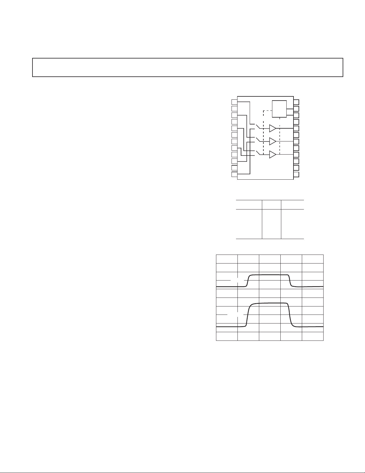
FUNCTIONAL BLOCK DIAGRAM
1
IN0A
D
IN1A
V
IN2A
IN2B
IN1B
IN0B
GND
REF
V
V
V
V
2
3
4
5
6
CC
7
EE
8
9
EE
10
11
EE
12
AD8186/AD8187
SELECT
LOGIC
ENABLE
0
1
2
Table I. Truth Table
SEL A/B OE OUT
00High Z
10High Z
11IN A
01IN B
24
23
22
21
20
19
18
17
16
15
14
13
V
CC
OE
SEL A/B
V
CC
OUT 0
V
EE
OUT 1
V
CC
OUT 2
V
EE
DV
CC
V
CC
GENERAL DESCRIPTION
The AD8186 (G = +1) and AD8187 (G = +2) are high speed,
single-supply, triple 2-to-1 multiplexers. They offer –3 dB large signal
bandwidth of over 480 MHz along with a slew rate in excess of
1500 V/µs. With better than –80 dB of all hostile crosstalk and
–95 dB OFF isolation, they are suited for many high speed applica
tions. The differential gain and differential phase error of 0.05%
and 0.05°, along with 0.1 dB flatness to 85 MHz, make the
AD8186 and AD8187 ideal for professional and component video
multiplexing. They offer 4 ns switching time, making
excellent choice for switching video signals while consuming less
than 20 mA on a single 5 V supply (100 mW
high speed disable feature that sets
impedance state. This allows the building of larger input arrays
while minimizing OFF channel output loading. The devices are
offered in a 24-lead TSSOP package.
REV. A
Information furnished by Analog Devices is believed to be accurate and
reliable. However, no responsibility is assumed by Analog Devices for its
use, nor for any infringements of patents or other rights of third parties that
may result from its use. No license is granted by implication or otherwise
under any patent or patent rights of Analog Devices. Trademarks and
registered trademarks are the property of their respective companies.
them an
). Both devices have a
the outputs into a high
Figure 1. AD8187 Video Amplitude Pulse
Response, V
= 1.4 V p-p, RL = 150
OUT
One Technology Way, P.O. Box 9106, Norwood, MA 02062-9106, U.S.A.
Tel: 781/329-4700 www.analog.com
Fax: 781/326-8703 © 2003 Analog Devices, Inc. All rights reserved.
Ω
Page 2

(TA = 25C; AD8186: VS = 5 V, RL = 1 k to 2.5 V; AD8187: VS = 5 V,
AD8186/AD8187–SPECIFICATIONS
V
= 2.5 V, RL = 150 to 2.5 V; unless otherwise noted.)
REF
AD8186/AD8187
Parameter Conditions Min Typ Max Unit
DYNAMIC PERFORMANCE
–3 dB Bandwidth (Small Signal) V
–3 dB Bandwidth (Large Signal) V
0.1 dB Flatness V
Slew Rate (10% to 90% Rise Time) V
Settling Time to 0.1% V
= 200 mV p-p 1000/1000 MHz
OUT
= 2 V p-p 450/480 MHz
OUT
= 200 mV p-p 90/85 MHz
OUT
= 2 V p-p, RL = 150 Ω 1600/1500 V/s
OUT
= 1 V Step, RL = 150 Ω 6/7.5 ns
IN
NOISE/DISTORTION PERFORMANCE
Differential Gain 3.58 MHz, RL = 150 Ω 0.05/0.05 %
Differential Phase 3.58 MHz, R
= 150 Ω 0.05/0.05 Degrees
L
All Hostile Crosstalk 5 MHz –84/–78 dB
100 MHz –52/–48 dB
Channel-to-Channel Crosstalk, RTI 5 MHz –90/–85 dB
OFF Isolation 5 MHz –84/–95 dB
Voltage Noise, RTI f = 100 kHz to 100 MHz 7/9 nV/√Hz
DC PERFORMANCE
Voltage Gain Error No Load 0.1/0.1 ⫾0.3/0.6 %
Voltage Gain Error Matching Channel A to Channel B 0.04/0.04 ⫾0.2/0.2 %
Gain Error 1 kΩ Load 0.04 ⫾0.6 %
V
REF
Input Offset Voltage 0.2/0.5 ⫾6.5/7.0 mV
to T
T
MIN
MAX
⫾8.0 mV
Input Offset Voltage Matching Channel A to Channel B 0.2/0.2 ⫾5.0/5.5 mV
Input Offset Drift 10/5 V/ºC
Input Bias Current 1.5/1.5 4/4 A
V
Bias Current (for AD8187 only) 1.0 A
REF
INPUT CHARACTERISTICS
Input Resistance @100 kHz 1.8/1.3 MΩ
Input Capacitance 0.9/1.0 pF
Input Voltage Range (About Midsupply) IN0A, IN0B, IN1A, IN1B,
IN2A, IN2B ⫾1.2/⫾1.2 V
V
REF
+0.9, –1.2 V
OUTPUT CHARACTERISTICS
Output Voltage Swing RL = 1 kΩ 3.1/2.8 3.2/3.0 V p-p
= 150 Ω 2.8/2.5 3.0/2.7 V p-p
R
L
Short Circuit Current 85 mA
Output Resistance Enabled @ 100 kHz 0.2/0.35 Ω
Disabled @ 100 kHz 1000/600 kΩ
Output Capacitance Disabled 1.5/2.0 pF
POWER SUPPLY
Operating Range 3.5 5.5 V
Power Supply Rejection Ratio +PSRR, V
= 0 V –72/–61 dB
V
EE
–PSRR, V
= 5.0 V –76/–72 dB
V
CC
= 4.5 V to 5.5 V,
CC
= –0.5 V to +0.5 V,
EE
Quiescent Current All Channels ON 18.5/19.5 21.5/22.5 mA
All Channels OFF 3.5/4.5 4.5/5.5 mA
T
MIN
to T
, All Channels ON 15 23 mA
MAX
REV. A–2–
Page 3

AD8186/AD8187
AD8186/AD8187
Parameter Conditions Min Typ Max Unit
SWITCHING CHARACTERISTICS
Channel-to-Channel Switching Time 50% Logic to 50% Output
Settling, INA = +1 V, INB = –1 V 3.6/4 ns
ENABLE to Channel ON Time 50% Logic to 50% Output
Settling, INPUT = 1 V 4/3.8 ns
DISABLE to Channel OFF Time 50% Logic to 50% Output
Settling, INPUT = 1 V 17/5 ns
Channel Switching Transient (Glitch) All Channels Grounded 21/45 mV
Output Enable Transient (Glitch) All Channels Grounded 64/118 mV
DIGITAL INPUTS
Logic 1 Voltage SEL A/B, OE Inputs 1.6 V
Logic 0 Voltage SEL A/B, OE Inputs 0.6 V
Logic 1 Input Current SEL A/B, OE = 2.0 V 45 nA
Logic 0 Input Current SEL A/B, OE = 0.5 V 2 A
OPERATING TEMPERATURE RANGE
Temperature Range Operating (Still Air) –40 +85 ºC
JA
JC
Specifications subject to change without notice.
Operating (Still Air) 85 ºC/W
Operating 20 ºC/W
REV. A
–3–
Page 4
AD8186/AD8187
IN0A
D
GND
V
REF
OUT 0
OUT 1
OUT 2
IN1A
IN2A
IN2B
IN1B
IN0B
V
CC
V
EE
V
EE
V
EE
V
CC
OE
SEL A/B
V
EE
V
CC
V
CC
V
CC
V
EE
DV
CC
24
23
22
21
20
19
18
17
16
15
14
13
1
2
3
4
5
6
7
8
9
10
11
12
AD8186/
AD8187
TOP VIEW
(Not to Scale)
ABSOLUTE MAXIMUM RATINGS
1, 2, 3, 4
Supply Voltage . . . . . . . . . . . . . . . . . . . . . . . . . . . . . . . . . 5.5 V
to D
DV
CC
DV
to VEE . . . . . . . . . . . . . . . . . . . . . . . . . . . . . . . . . . 8.0 V
CC
to D
V
CC
IN0A, IN0B, IN1A, IN1B, IN2A, IN2B, V
SEL A/B, OE . . . . . . . . . . . . . . . . . . . . . . D
. . . . . . . . . . . . . . . . . . . . . . . . . . . . . . . . . 5.5 V
GND
. . . . . . . . . . . . . . . . . . . . . . . . . . . . . . . . . . 8.0 V
GND
. . . VEE ≤ VIN ≤ V
REF
GND
≤ V
IN
≤ DV
CC
CC
Output Short Circuit Operation . . . . . . . . . . . . . . . Indefinite
Storage Temperature Range . . . . . . . . . . . . –65ºC to +150ºC
Lead Temperature Range (Soldering 10 sec) . . . . . . . . . 300ºC
NOTES
1
Stresses above those listed under Absolute Maximum Ratings may cause permanent damage to the device. This is a stress rating only; functional operation of the
device at these or any other conditions above those indicated in the Theory of
Operation section of this specification is not implied. Exposure to absolute
maximum rating conditions for extended periods may affect device reliability.
2
Specification is for device in free air (TA = 25ºC).
3
24-lead TSSOP; TJA= 85ºC/W. Maximum internal power dissipation (PD) should be
derated for ambient temperature (TA) such that PD < (150ºC TA)/TJA.
4
TJA of 85⬚C/W is on a 4-layer board (2s 2p).
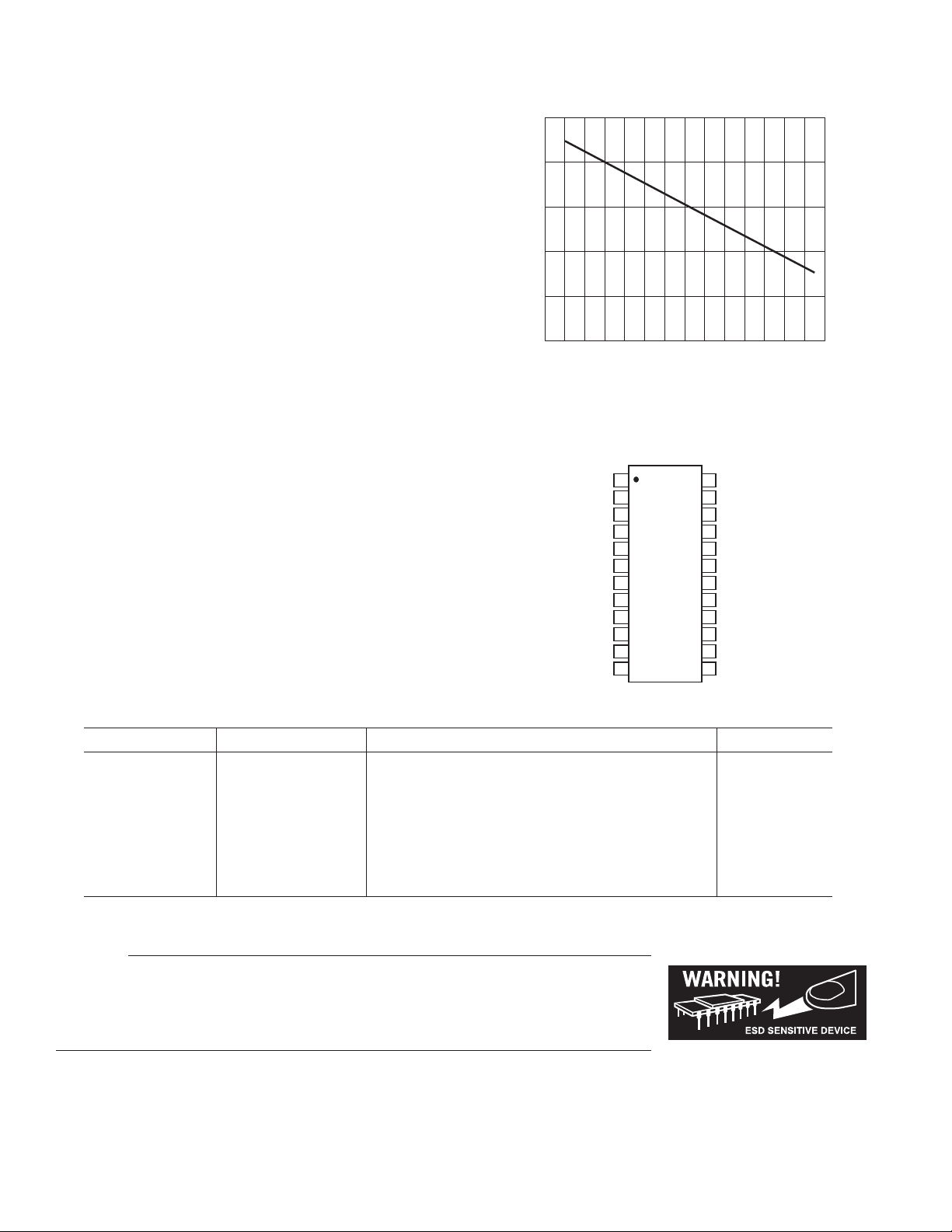
MAXIMUM POWER DISSIPATION
The maximum safe junction temperature for plastic encapsulated
devices is determined by the glass transition temperature of the
plastic, approximately 150ºC. Temporarily exceeding this limit
may cause a shift in parametric performance due to a change in
the stresses exerted on the die by the package. Exceeding a
junction temperature of 175ºC for an extended period can result
in device failure.
While the AD8186/AD8187 is internally short circuit protected,
this may not be sufficient to guarantee that the maximum junction
temperature (150ºC) is not exceeded under all conditions. To
ensure proper operation, it is necessary to observe the maximum
power derating curves shown in Figure 2.
2.5
2.0
1.5
1.0
0.5
MAXIMUM POWER DISSIPATION (W)
0
–50 –40
–30 –20 –10 0 10 20 30 40 50 60 70 80 90
AMBIENT TEMPERATURE (C)
Figure 2. Maximum Power Dissipation vs. Temperature
PIN CONFIGURATION
ORDERING GUIDE
Model Temperature Range Package Description Package Option
AD8186ARU –40ºC to +85ºC 24-Lead Thin Shrink Small Outline Package (TSSOP) RU-24
AD8186ARU-REEL –40ºC to +85ºC 13" Reel TSSOP RU-24
AD8186ARU-REEL 7
–40ºC to +85ºC 7" Reel TSSOP RU-24
AD8187ARU –40ºC to +85ºC 24-Lead Thin Shrink Small Outline Package (TSSOP) RU-24
AD8187ARU-REEL –40ºC to +85ºC 13" Reel TSSOP RU-24
AD8187ARU-REEL 7
–40ºC to +85ºC 7" Reel TSSOP RU-24
AD8186-EVAL Evaluation Board
AD8187-EVAL Evaluation Board
CAUTION
ESD (electrostatic discharge) sensitive device. Electrostatic charges as high as 4000 V readily
accumulate on the human body and test equipment and can discharge without detection. Although the
AD8186/AD8187 features proprietary ESD protection circuitry, permanent damage may occur on
devices subjected to high energy electrostatic discharges. Therefore, proper ESD precautions are
recommended to avoid performance degradation or loss of functionality.
REV. A–4–
Page 5
Typical Performance Characteristics–
FREQUENCY (MHz)
NORMALIZED GAIN (dB)
0.1 1.0 10.0 100.0 1000.0
1
0
–1
–2
–3
–4
–5
–6
AD8186/AD8187
3
2
50
1
0
–1
–2
GAIN (dB)
–3
–4
–5
–6
0.1 1.0 10.0 100.0 1000.0
976
DUT
FREQUENCY (MHz)
52.3
GAIN
FLATNESS
TPC 1. AD8186 Frequency Response,
V
= 200 mV p-p, RL = 1 k
OUT
1
0
–1
–2
–3
–4
GAIN (dB)
–5
–6
–7
–8
150 976
50
0.1 1.0 10.0 100.0 1000.0
DUT
52.3
FREQUENCY (MHz)
Ω
10000.0
0.6
0.5
0.4
0.3
0.2
0.1
0
–0.1
–0.2
–0.3
FLATNESS (dB)
1
0
–1
–2
–3
–4
NORMALIZED GAIN (dB)
–5
–6
0.1 1.0 10.0 100.0 1000.0
GAIN
FLATNESS
FREQUENCY (MHz)
TPC 4. AD8187 Frequency Response,
= 200 mV p-p, RL = 150
V
OUT
Ω
0
10000.0
0.5
0.4
0.3
0.2
0.1
NORMALIZED FLATNESS (dB)
–0.1
–0.2
TPC 2. AD8186 Frequency Response,
= 2 V p-p, RL = 1 k
V
OUT
1
0
–1
–2
–3
–4
NORMALIZED GAIN (dB)
–5
–6
150 976
50
0.1 1.0 10.0 100.0 1000.0
DUT
FREQUENCY (MHz)
Ω
+85C
+25C
–40C
52.3
TPC 3. AD8186 Large Signal Bandwidth vs.
Temperature, V
= 2 V p-p, RL = 1 k
OUT
Ω
TPC 5. AD8187 Frequency Response,
= 2 V p-p, RL = 150
V
OUT
1
0
–1
–2
–3
–4
NORMALIZED GAIN (dB)
–5
–6
0.1 1.0 10.0 100.0 1000.0
FREQUENCY (MHz)
Ω
–40C
+85C
+25C
TPC 6. AD8187 Large Signal Bandwidth vs.
Temperature, V
= 2 V p-p, RL = 150
OUT
Ω
REV. A
–5–
Page 6
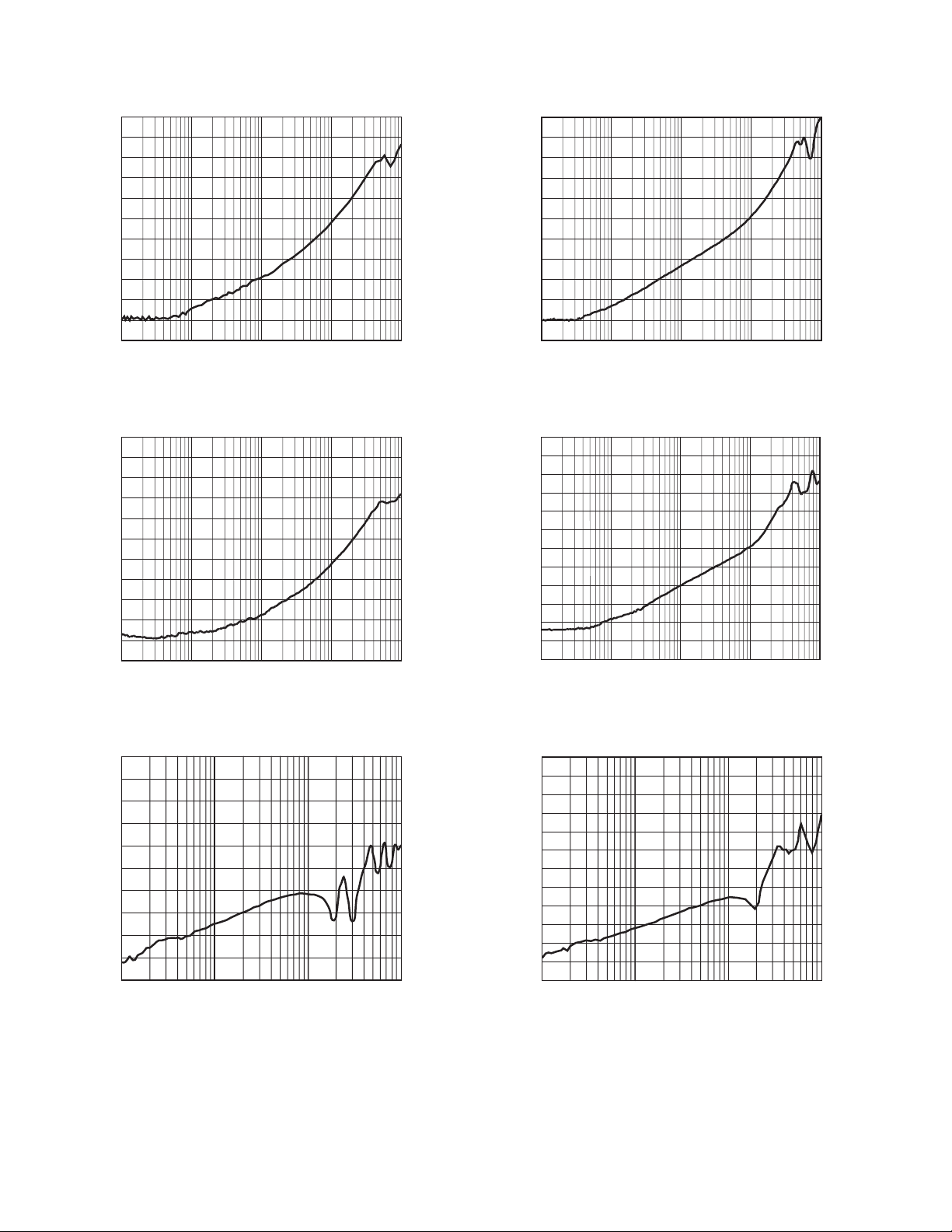
AD8186/AD8187
0
–10
–20
–30
–40
–50
–60
–70
CROSSTALK (dB)
–80
–90
–100
–110
0.1
110100 1000
FREQUENCY (MHz)
TPC 7. AD8186 All Hostile Crosstalk* vs. Frequency
0
–10
–20
–30
–40
–50
–60
–70
CROSSTALK (dB)
–80
–90
–100
–110
0.1
1.0 10.0 100.0 1000.0
FREQUENCY (MHz)
TPC 8. AD8186 Adjacent Channel Crosstalk* vs. Frequency
0
–10
–20
–30
–40
–50
–60
–70
CROSSTALK (dB)
–80
–90
–100
–110
0.1
1.0 10.0 100.0 1000.0
FREQUENCY (MHz)
TPC 10. AD8187 All Hostile Crosstalk* vs. Frequency
0
–10
–20
–30
–40
–50
–60
–70
CROSSTALK (dB)
–80
–90
–100
–110
–120
0.1
1.0 10.0 100.0 1000.0
FREQUENCY (MHz)
TPC 11. AD8187 Adjacent Channel Crosstalk* vs. Frequency
0
–10
–20
–30
–40
–50
–60
OFF ISOLATION (dB)
–70
–80
–90
–100
0
10
FREQUENCY (MHz)
100 1000
TPC 9. AD8186 OFF Isolation* vs. Frequency
0
–10
–20
–30
–40
–50
–60
–70
–80
OFF ISOLATION (dB)
–90
–100
–110
–120
110100 1000
TPC 12. AD8187 OFF Isolation* vs. Frequency
* All hostile crosstalk—Drive all INA, listen to output with INB selected.
Adjacent channel crosstalk—Drive one INA, listen to an adjacent output with INB selected.
Off isolation—Drive inputs with OE tied low.
FREQUENCY (MHz)
REV. A–6–
Page 7

AD8186/AD8187
FREQUENCY (MHz)
0.01 0.10 1 10 100
PSRR (dB)
–80
–70
–60
–50
–40
–30
–20
–10
0
–PSRR
+PSRR
FREQUENCY (MHz)
NOISE (nV/ Hz)
0.01 0.1 1 10 100
20
10
8
6
4
2
0
10000
18
16
14
12
1000
0
–10
–20
–30
–40
–50
–60
DISTORTION (dBc)
–70
–80
–90
–100
1
FREQUENCY (MHz)
THIRD
SECOND
10
100
TPC 13. AD8186 Harmonic Distortion vs. Frequency
V
= 2 V p-p, RL = 150
OUT
0
–10
–20
–30
–40
–50
PSRR (dB)
–60
–70
–80
–90
0.01 0.10 1 10 100
Ω
–PSRR
+PSRR
FREQUENCY (MHz)
0
–10
–20
–30
–40
–50
–60
DISTORTION (dBc)
–70
–80
–90
–100
1
FREQUENCY (MHz)
10
THIRD
SECOND
100
TPC 16. AD8187 Harmonic Distortion vs. Frequency
V
= 2 V p-p, RL = 150
OUT
Ω
TPC 14. AD8186 PSRR vs. Frequency, RL = 150
20
18
16
14
12
10
8
NOISE (nV/ Hz)
6
4
REV. A
2
0
0.01 0.10 1 10 100
FREQUENCY (MHz)
TPC 15. AD8186 Input Voltage Noise vs. Frequency
1000
Ω
10000
–7–
TPC 17. AD8187 PSRR vs. Frequency, RL = 150
Ω
TPC 18. AD8187 Input Voltage Noise vs. Frequency
Page 8

AD8186/AD8187
10000
1000
100
10
IMPEDANCE (k)
1
0.1
0.1 1 10 100
FREQUENCY (MHz)
1000
TPC 19. AD8186 Input Impedance vs. Frequency
1000
100
10
10000
1000
100
10
IMPEDANCE (k)
1
0.1
0.1 1.0 10.0 100.0
FREQUENCY (MHz)
1000.0
TPC 22. AD8187 Input Impedance vs. Frequency
1000
100
10
IMPEDANCE ()
1
0.1
0.1 1 10 100
FREQUENCY (MHz)
1000
TPC 20. AD8186 Enabled Output Impedance vs. Frequency
10000
1000
100
10
IMPEDANCE (k)
1
0.1
0.1 1.0 10.0 100.0
FREQUENCY (MHz)
1000.0
TPC 21. AD8186 Disabled Output Impedance vs. Frequency
IMPEDANCE ()
1
0.1
0.1 1.0 10.0 100.0
TPC 23. AD8187
10000
1000
100
10
IMPEDANCE ()
1
0.1
0.1 1.0 10.0 100.0
FREQUENCY (MHz)
Enabled Output Impedance vs. Frequency
FREQUENCY (MHz)
1000.0
1000.0
TPC 24. AD8187 Disabled Output Impedance vs. Frequency
REV. A–8–
Page 9

AD8186/AD8187
TIME (ns)
OUTPUT VOLTAGE (V)
05
10
3.2
3.1
INPUT VOLTAGE (V)
2.5
3.0
2.9
2.8
2.7
2.6
2.4
2.3
2.2
2.1
2.0
2.6
1.9
1.8
2.7
2.8
2.5
2.4
2.3
2.2
INPUT
OUTPUT
15 20
25
TIME (ns)
OUTPUT VOLTAGE (V)
05
10
6.0
5.5
INPUT VOLTAGE (V)
2.5
4.5
4.0
3.5
3.0
2.5
2.0
1.5
1.0
0.5
0
3.0
–0.5
–1.0
3.5
4.0
2.0
1.5
1.0
INPUT
OUTPUT
15 20
5.0
25
TIME (ns)
OUTPUT VOLTAGE (V)
0
6.0
5.5
INPUT VOLTAGE (V)
2.5
4.5
4.0
3.5
3.0
2.5
2.0
1.5
1.0
0.5
0
3.0
–0.5
–1.0
3.5
4.0
2.0
1.5
1.0
INPUT
OUTPUT
5.0
–1.5
0.5
–2.0
0
5101520
25
2.80
2.70
2.60
2.50
2.40
2.30
2.20
INPUT VOLTAGE (V)
2.10
2.00
1.90
1.80
051015 20
INPUT
OUTPUT
TIME (ns)
TPC 25. AD8186 Small Signal Pulse Response,
V
= 200 mV p-p, RL = 1 k
OUT
3.0
2.5
2.0
1.5
1.0
INPUT
Ω
3.30
2.80
OUTPUT VOLTAGE (V)
2.30
25
TPC 28. AD8187 Small Signal Pulse Response,
V
4.0
3.5
3.0
5.0
4.5
= 200 mV p-p, RL = 150 k
OUT
Ω
REV. A
INPUT VOLTAGE (V)
0.5
0
–0.5
–1.0
OUTPUT
051015 20
TIME (ns)
TPC 26. AD8186 Video Signal Pulse Response,
= 700 mV p-p, RL = 1 k
V
OUT
4.0
INPUT VOLTAGE (V)
3.5
3.0
2.5
2.0
1.5
1.0
0.5
0
–0.5
–1.0
–1.5
–2.0
INPUT
OUTPUT
051015 20
TPC 27. AD8186 Large Signal Pulse Response,
= 2 V p-p, RL = 1 k
V
OUT
TIME (ns)
Ω
Ω
2.5
OUTPUT VOLTAGE (V)
2.0
1.5
1.0
25
TPC 29. AD8187 Video Amplitude Pulse
Response, V
7.0
6.5
6.0
5.5
5.0
4.5
4.0
3.5
3.0
OUTPUT VOLTAGE (V)
2.5
2.0
1.5
1.0
25
= 1.4 V p-p, RL = 150 k
OUT
Ω
TPC 30. AD8187 Large Signal Pulse Response,
V
= 2 V p-p, RL = 150 k
OUT
Ω
–9–
Page 10

AD8186/AD8187
TIME (ns)
OUTPUT AMPLITUDE (V)
05 1015
20
2.80
SELECT A/
B
PULSE AMPLITUDE (V)
1.50
2.70
2.60
0.50
–0.50
2.00
2.50
2.40
OUTPUT
–1.00
SEL A/B
25 30 35 40
45
1.00
0
2.90
3.00
50
t
SETTLED
OUTPUT (1mV/DIV)
t
0
TIME (2ns/DIV)
TPC 31. AD8186 Settling Time (0.1%),
= 2 V Step, RL = 1 k
V
OUT
2.3
1.8
SEL A/B
1.3
0.8
0.3
–0.3
–0.8
–1.3
–1.8
SELECT A/B PULSE AMPLITUDE (V)
–2.3
–2.8
051015 20
OUTPUT
Ω
25
TIME (ns)
TPC 32. AD8186 Channel-to-Channel Switching
Time, V
= 2 V p-p, INA = 3.5 V, INB = 1.5 V
OUT
6.0
5.5
5.0
4.5
4.0
3.5
3.0
2.5
OUTPUT AMPLITUDE (V)
2.0
1.5
1.0
t
SETTLED
OUTPUT (1mV/DIV)
t
0
TIME (2ns/DIV)
TPC 34. AD8187 Settling Time (0.1%),
= 2 V Step, RL = 150
V
OUT
2.0
1.5
1.0
0.5
0
–0.5
–1.0
–1.5
SELECT A/B PULSE AMPLITUDE (V)
–2.0
–2.5
051015 20
SEL A/B
OUTPUT
TIME (ns)
Ω
5.5
5.0
4.5
4.0
3.5
3.0
2.5
2.0
1.5
1.0
25
TPC 35. AD8187 Channel-to-Channel Switching
Time, V
= 2 V p-p, INA = 3.0 V, INB = 2.0 V
OUT
OUTPUT AMPLITUDE (V)
2.0
1.5
1.0
0.5
0
–0.5
SELECT A/B PULSE AMPLITUDE (V)
–1.0
TPC 33. AD8186 Channel Switching Transient (Glitch),
INA = INB = 0 V
SEL A/B
OUTPUT
051015
25 30 35 40
20
TIME (ns)
3.0
2.9
2.8
2.7
2.6
OUTPUT AMPLITUDE (V)
2.5
2.4
50
45
TPC 36. AD8187 Channel Switching Transient
(Glitch), INA = INB = V
REF
= 0 V
REV. A–10–
Page 11

AD8186/AD8187
)
TIME – ns
OUTPUT AMPLITUDE (V)
04080120 160
OE PULSE AMPLITUDE (V)
2.0
1.5
1.0
0.5
0
–0.5
–1.0
–1.5
OUTPUT
–2.0
6.0
5.0
4.0
3.0
2.0
5.5
4.5
3.5
2.5
OE
200
(
)
2.0
1.5
1.0
0.5
–0.5
OE PULSE AMPLITUDE (V)
–1.0
–1.5
OE
0
OUTPUT
04080120 160
TIME (ns
TPC 37. AD8186 Enable ON/OFF Time,
= 0 V to 1 V
V
OUT
1.5
1.0
OE
5.5
5.0
4.5
4.0
3.5
3.0
OUTPUT AMPLITUDE (V)
2.5
2.0
200
3.0
2.9
2.8
2.7
TPC 39. AD8187 Enable ON/OFF Time,
= 0 V to 1 V
V
OUT
2.00
1.50
1.00
0.50
OE
3.00
2.90
2.80
2.70
V
0.5
OE PULSE AMPLITUDE (V)
0
051015 20
OUTPUT
25 30 35 40
TIME (ns)
TPC 38. AD8186 Channel Enable/Disable
Transient (Glitch)
2.6
OUTPUT AMPLITUDE (V)
2.5
2.4
50
45
0
OE PULSE AMPLITUDE (V)
–0.50
–1.00
OUTPUT
0102030 40
515253545
TIME (ns)
2.60
OUTPUT AMPLITUDE
2.50
2.40
50
TPC 40. AD8187 Channel Enable/Disable
Transient (Glitch)
REV. A
–11–
Page 12

AD8186/AD8187
THEORY OF OPERATION
The AD8186 (G = +1) and AD8187 (G = +2) are single-supply,
triple 2:1 multiplexers with TTL compatible global
ing and output-enable control. Optimized for select
input switch-
ing between
two RGB (red, green, blue) video sources, the devices have high
peak slew rates, maintaining their bandwidth for large signals.
Additionally, the multiplexers are compensated for high phase
margin, minimizing overshoot for good pixel resolution. The
multiplexers also have respectable video specifications and are
superior for switching NTSC or PAL composite signals.
The multiplexers are organized as three independent channels,
each with two input transconductance stages and one output
transimpedance stage. The appropriate input transconductance
stages are selected via one logic pin (SEL A/B) such that all
three outputs switch input connections simultaneously. The
unused input stages are disabled with a proprietary clamp circuit to provide excellent crosstalk isolation between “on” and
“off” inputs while protecting the disabled devices from damaging reverse base-emitter voltage stress. No additional input
buffering is necessary, resulting in low input capacitance and
high input impedance without additional signal degradation.
The transconductance stage, a high slew rate, class AB circuit,
sources signal current into a high impedance node. Each output
stage contains a compensation network and is buffered to the
output by a complementary emitter-follower stage. Voltage
feedback sets the gain, with the AD8186 configured as a unity
gain follower and the AD8187 as a gain-of-two amplifier with a
feedback network. This architecture provides drive for a reverseterminated video load (150 ⍀) with low differential gain and
phase errors while consuming relatively little power. Careful
chip layout and biasing result in excellent crosstalk isolation
between channels.
High Impedance, Output Disable Feature, and Off Isolation
The output-enable logic pin (OE) controls whether the three
outputs are enabled or disabled to a high impedance state.
The high impedance disable allows larger matrices to be built
by busing the outputs together. In the case of the AD8187
(G = +2), a feedback isolation scheme is used so that the
impedance of the gain-of-two feedback network does not load
the output. When not in use, the outputs can be disabled to
reduce power consumption.
The reader may have noticed that the off isolation performance of
the signal path is dependent upon the value of the load resistor,
RL. For calculating off isolation, the signal path may be modeled
as a simple high-pass network with an effective capacitance of
3 fF. Off isolation will improve as the load resistance is decreased. In
the case of the AD8186, off isolation is specified with a 1 kΩ
load. However, a practical application would likely gang the
outputs of multiple muxes. In this case, the proper load resistance
for the off isolation calculation is the output impedance of an
enabled AD8186, typically less than a 10th of an ohm.
Full Power Bandwidth vs. –3 dB Large Signal Bandwidth
Note that full power bandwidth for an undistorted sinusoidal signal
is often calculated using the peak slew rate from the equation
Full Power Bandwidth =
Peak Slew Rate
Sinusoid Amplitude2π×
The peak slew rate is not the same as the average slew rate. The
average slew rate is typically specified as the ratio
∆∆V
OUT
t
measured between the 20% to 80% output levels of a sufficiently large output pulse. For a natural response, the peak slew
rate may be 2.7 times larger than the average slew rate. Therefore, calculating a full power bandwidth with a specified average
slew rate will give a pessimistic result. In specifying the large
signal performance of these multiplexers, we’ve published the
large-signal bandwidth, the average slew rate, and the measurements of the total harmonic distortion. (Large signal bandwidth
is defined as the –3 dB point measured on a 2 V p-p output
sine wave.) Specifying these three aspects of the signal path’s
large signal dynamics allows the user to predict system behavior
for either pulse or sinusoid waveforms.
Single-Supply Considerations
DC-Coupled Inputs, Integrated Reference Buffers, and
Selecting the V
Level on the AD8187, (G = +2)
REF
The AD8186 and AD8187 offer superior large signal dynamics.
The trade-off is that the input and output compliance is limited
to ~1.3 V from either rail when driving a 150 ⍀ load. These
sections address some challenges of designing video systems
within a single 5 V supply.
The AD8186
The AD8186 is internally wired as a unity-gain follower. Its
inputs and outputs can both swing to within ~1.3 V of either
rail. This affords the user 2.4 V of dynamic range at input and
output, which should be enough for most video signals, whether
the inputs are ac- or dc-coupled. In both cases, the choice of
output termination voltage will determine the quiescent load
current.
For improved supply rejection, the V
pin should be tied to
REF
an ac ground (the more quiet supply is a good bet). Internally,
the V
pin connects to one terminal of an on-chip capacitor.
REF
The capacitor’s other terminal connects to an internal node.
The consequence of building this bypass capacitor on-chip is
twofold. First, the V
pin on the AD8186 draws no input bias
REF
current. (Contrast this to the case of the AD8187, where the
pin typically draws 2 µA of input bias current). Second,
V
REF
on the AD8186, the V
pin may be tied to any voltage within
REF
the supply range.
AD8186
IN0A
IN0B
IN1A
IN1B
IN2A
IN2B
V
REF
DIRECT CONNECTION TO ANY “QUIET” AC GROUND
(FOR EXAMPLE, GND, V
Figure 3. V
REF
MUX SYSTEM
OUT0
OUT1
OUT2
“C_BYPASS”
INTERNAL CAP
BIAS REFERENCE
, V
CC
EE)
Pin Connection for AD8186 (Differs
from AD8187)
REV. A–12–
Page 13

AD8186/AD8187
The AD8187
The AD8187 uses on-chip feedback resistors to realize the gainof-two function. To provide low crosstalk and a high output
impedance when disabled, each set of 500 Ω feedback resistors is
terminated by a dedicated reference buffer. A reference buffer is
a high speed op amp configured as a unity-gain follower. The
three reference buffers, one for each channel, share a single, high
impedance input, the V
pin (see Figure 4). V
REF
input bias
REF
current is typically less than 2 µA.
A0
B0
V
REF
5V
5V
5V
GBUF 0
5V
GBUF 1
500 500
5V
GBUF 2
500 500
VF-1
VF-2
1
OUT 0
500
VFO
500
OUT1
OUT2
Figure 4. Conceptual Diagram of a Single
Multiplexer Channel, G = +2
This configuration has a few implications for single-supply
operation:
1) On the AD8187, V
analog supply, V
may not be tied to the most negative
REF
.
EE
Limits on Reference Voltage (AD8187, see Figure 5):
VVVVV
+<<
13 16
.–.
EE REF CC
VV Von V / V Supplies
<<
13 34 0 5
..
A0
V
REF
REF
V
5V
V
O_MAX
V
O_MIN
GND
5V
V
O_MAX
REF
V
O_MIN
GND
V
OUT
= 1.3V
= 1.3V
= 3.7V
= 3.4V
5V
OUT 0
5V
1.3V
1.3V
1.6V
1.3V
Figure 5. Output Compliance of Main Amplifier
Channel and Ground Buffer
2) Signal at the V
should be tied to a well bypassed, low impedance source.
V
REF
pin appears at each output. Therefore,
REF
Using superposition, it is easily shown that
3) To maximize the output dynamic range, the reference voltage
should be chosen with some care.
For example, consider amplifying a 700 mV video signal with a
sync pulse 300 mV below black level. The user might decide to set
V
at black level to preferentially run video signals on the faster
REF
NPN transistor path. The AD8186 would, in this case, allow a
reference voltage as low as 1.3 V + 300 mV = 1.6 V. If the AD8187
is used, the sync pulse would be amplified to 600 mV. Therefore,
the lower limit on V
becomes 1.3 V + 600 mV = 1.9 V. For
REF
routing RGB video, an advantageous configuration would be to
employ +3 V and –2 V supplies, in which case V
could be
REF
tied to ground.
If system considerations prevent running the multiplexer on split
supplies, a false ground reference should be employed. A low
impedance reference may be synthesized with a second operational amplifier. Alternately, a well bypassed resistor divider
may serve. Refer to the Application section for further explana-
and more examples.
tion
5V
10k
100k
GND
OP21
1F
FROM 1992 ADI AMPLIFIER
APPLICATIONS GUIDE
0.022F
100
1F
V
REF
Figure 6a. Synthesis of a False Ground Reference
5V
10k
V
REF
10k
CAP MUST BE LARGE
ENOUGH TO ABSORB
TRANSIENT CURRENTS
WITH MINIMUM BOUNCE.
1F
Figure 6b. Alternate Method for Synthesis of a
False Ground Reference
High Impedance Disable
Both the AD8186 and the AD8187 may have their outputs
disabled to a high impedance state. In the case of the AD8187,
the reference buffers also disable to a state of high output
impedance. This feature prevents the feedback network of a
disabled channel from loading the output, which is valuable
when busing together the outputs of several muxes.
REV. A
VVV
=×2–
OUT IN REF
–13–
Page 14

AD8186/AD8187
AC-Coupled Inputs (DC Restore before Mux Input)
Using ac-coupled inputs presents an interesting challenge for video
systems operating from a single 5 V supply. In NTSC and PAL
video systems, 700 mV is the approximate difference between the
maximum signal voltage and black level. It is assumed that sync
has been stripped. However, given the two pathological cases
shown in Figure 7, a dynamic range of twice the maximum signal
swing is required if the inputs are to be ac-coupled. A possible
solution would be to use a dc restore circuit before the mux.
WHITE LINE WITH BLACK PIXEL
V
–700mV
+ V
SIGNAL
REF
+700mV
V
REF
BLACK LINE WITH WHITE PIXEL
+5 V
V
SIGNAL
GND
V
AVG
V
AVG
V
= V
INPUT
REF
V
~ V
REF
AVG
V
IS A DC VOLTAGE
REF
SET BY THE RESISTORS
Figure 7. Pathological Case for
Input Dynamic Range
Tolerance to Capacitive Load
Op amps are sensitive to reactive loads. A capacitive load at the
output appears in parallel with an effective resistance of R
), where RL is the discrete resistive load, and rO is the open-
(R
L储rO
EFF
=
loop output impedance, approximately 15 Ω for these muxes.
The load pole, at f
LOAD
= 1/(2 R
), can seriously degrade
EFF CL
phase margin and therefore stability. The old workaround is to
place a small series resistance directly at the output to isolate the
load pole. While effective, this ruse also affects the dc and termination characteristics of a 75 Ω system. The AD8186 and AD8187
are built with a variable compensation scheme that senses the
output reactance and trades bandwidth for phase margin, ensuring
faster settling and lower overshoot at higher capacitive loads.
Secondary Supplies and Supply Bypassing
The high current output transistors are given their own supply
pins (Pins 15, 17, 19, and 21) to reduce supply noise on-chip
and to improve output isolation. Since these secondary, high
current supply pins are not connected on-chip to the primary
analog supplies (V
, Pins 6, 7, 9, 11, 13, and 24), some
CC/VEE
care should be taken to ensure that the supply bypass capacitors
are connected to the correct pins. At a minimum, the primary
supplies should be bypassed. Pin 6 and Pin 7 may be a convenient
place to accomplish this. Stacked power and ground planes could
be a convenient way to bypass the high current supply pins.
0.1F
1F
IN0A
D
GND
IN1A
V
IN2A
V
IN2B
IN1B
V
IN0B
REF
V
V
1
2
3
4
5
6
CC
7
EE
8
9
EE
10
11
EE
12
MUX0
MUX1
MUX2
24
23
22
21
20
19
18
17
16
15
14
13
V
CC
OE
SEL A/B
V
CC
OUT 0
V
EE
OUT 1
V
CC
OUT 2
V
EE
DV
CC
V
CC
Figure 8. Detail of Primary and Secondary Supplies
Split-Supply Operation
Operating from split supplies (e.g., +3 V/–2 V or ±2.5 V) simplifies the selection of the V
voltage.
The logic
supplies and
powering the
In this case, it is convenient to tie V
inputs are level shifted internally to allow the digital
logic inputs to operate from 0 V and 5 V when
analog circuits from split supplies. The maximum
voltage difference between DV
voltage and load resistor termination
REF
and VEE must not exceed 8 V
CC
to ground.
REF
(see Figure 9).
SPLIT-SUPPLY OPERATION
DIGITAL SUPPLIES
(+5)
(0V)
DV
CC
8V MAX
D
GND
ANALOG SUPPLIES
(+2.5)
(–2.5)
V
CC
V
EE
Figure 9. Split-Supply Operation
REV. A–14–
Page 15

AD8186/AD8187
APPLICATION
Single-Supply Operation
The AD8186/AD8187 are targeted mainly for use in singlesupply 5 V systems. For operating on these supplies, both V
and D
be referenced to ground. Normally, the DV
should be tied to ground. The control logic pins will
GND
supply should be
CC
EE
set to the same positive supply as the driving logic.
For dc-coupled single-supply operation, it is necessary to set an
appropriate input dc level that is within the specified range of the
amplifier. For the unity-gain AD8186, the output dc level will
be the same as the input, while for the gain-of-two AD8187, the
V
input can be biased to obtain an appropriate output dc level.
REF
Figure 10 shows a circuit that provides a gain-of-two and is
dc-
coupled. The video input signals must have a dc bias
from their source of approximately 1.5 V. This same volt-
applied to V
age is
video signal is at 1.5 V, the output will also be at the
the
voltage. This is close to the lower dynamic range of
same
of the AD8187. The result is that when
REF
both the input and the output.
When the input goes most positive, which is 700 mV above the
black level for a standard video signal, it reaches a value of 2.2 V
and there is enough headroom for the signal. On the output
side, the magnitude of the signal will change by 1.4 V, which
will make the maximum output voltage 2.2 V + 1.4 V = 3.6 V.
This is just within the dynamic range of the output of the part.
AC Coupling
When a video signal is ac-coupled, the amount of dynamic range
required to handle the signal can potentially be double that
required for dc-coupled operation. For the unity-gain AD8186,
there is still enough dynamic range to handle an ac-coupled,
standard video signal with 700 mV p-p amplitude.
If the input is biased at 2.5 V dc, the input signal can potentially go
700 mV both above and below this point. The resulting 1.8 V and
2.2 V are within the input signal range for single 5 V operation.
Since the part is unity-gain, the outputs will follow the inputs,
and there will be adequate range at the output as well.
When using the gain-of-two AD8187 in a simple ac-coupled
application, there will be a dynamic range limitation at the output
caused by its higher gain. At the output, the gain-of-two will
produce a signal swing of 1.4 V, but the ac coupling will double
this required amount to 2.8 V. The AD8187 outputs can only
swing from 1.4 V to 3.6 V on a 5 V supply, so there are only
2.2 V of dynamic signal swing available at the output.
A standard means for reducing the dynamic range requirements
of an ac-coupled video signal is to use a dc restore. This circuit
works to limit the dynamic range requirements by clamping the
black level of the video signal to a fixed level at the input to the
amplifier. This prevents the video content of the signal from
varying the black level as happens in a simple ac-coupled circuit.
After ac coupling a video signal, it is always necessary to use a
dc restore to establish where the black level is. Usually, this
appears at the end of a video signal chain. This dc restore circuit
needs to have the required accuracy for the
sates for all the offsets of the preceding
system. It compen-
stages. Therefore, if a
dc restore circuit is to be used only for dynamic-range limiting,
it does not require great dc accuracy.
0.7V MAX
2.2V
1.5V
BLACK
LEVEL
TYPICAL INPUT LEVELS
(ALL 6 OUTPUTS)
REDA
GRNA
BLUA
3.48k
1.5k
REDB
GRNB
BLUB
3V TO 5V
IN0A
IN1A
IN2A
5V
1.5V
V
REF
IN0B
IN1B
IN2B
D
GND
5V
V
DV
CC
CC
AD8187
OUT0
OUT1
OUT2
OE
RED
3.0V
1.4V MAX
1.5V
GRN
BLACK
LEVEL
TYPICAL OUTPUT LEVELS
(ALL 3 OUTPUTS)
BLU
2
2
2
V
SEL A/B
EE
Figure 10. DC-Coupled (Bypassing and Logic Not Shown)
REV. A
–15–
Page 16

AD8186/AD8187
A dc restore circuit using the AD8187 is shown in Figure 11.
Two separate sources of RGB video are ac-coupled to the
µF input capacitors of the AD8187. The input points of
0.1
the
AD8187 are switched to a 1.5 V reference by the ADG786,
which works in the following manner:
The SEL A/B signal selects the A or B inputs to the AD8187. It
also selects the switch positions in the ADG786 such that the
same selected inputs will be connected to V
when EN is low.
REF
During the horizontal interval, all of the RGB input signals are at
a flat black level. A logic signal that is low during HSYNC is
applied to the EN of the ADG786. This closes the switches
clamps the black level to 1.5 V. At all other times, the switches
and
are off and the node at the inputs to the AD8187 floats.
There are two considerations for sizing the input coupling capacitors. One is the time constant during the H-pulse clamping. The
other is the droop associated with the capacitor discharge due to the
input bias current of the AD8187. For the former, it is better to
have a small capacitor; but for the latter, a larger capacitor is better.
The ON resistance of the ADG786 and the coupling capacitor
forms the time constant of the input clamp. The ADG786 ON
resistance is 5 Ω max. With a 0.1 µF capacitor, a time constant
of 0.5 µs is created. Thus, a sync pulse of greater than 2.5 µs will
cause less than 1% error. This is not critical because the
level from successive lines is very close and the voltage
black
changes
little from line to line.
A rough approximation for the horizontal line time for a graphics
system is 30 µs. This will vary depending on the resolution and
the vertical rate. The coupling capacitor needs to hold the voltage
relatively constant during this time while the input bias current
of the AD8187 is discharging it.
The change in voltage is I
the capacitance. With an I
times the line time divided by
BIAS
of 2.5 µA, a line time of 30 µs,
BIAS
and a 0.1 µF coupling capacitor, the amount of droop is
0.75 mV. This is roughly 0.1% of the full video amplitude and
will not be observable in the video display.
High Speed Design Considerations
The AD8186/AD8187 are extremely high speed switching amplifiers for routing the highest resolution graphic signals. Extra care
is required in the circuit design and layout to ensure that the full
resolution of the video is realized.
First, the board should have at least one layer of a solid ground
plane. Long signal paths should be referenced to a ground plane
as controlled-impedance traces. All bypass capacitors should be
very close to the pins of the part with absolutely minimum extra
circuit length in the path. It is also helpful to have a large V
CC
plane on a circuit board layer that is closely spaced to the ground
plane. This creates a low inductance interplane capacitance,
which is very helpful in supplying the fast transient currents that
the part demands during high resolution signal transitions.
Evaluation Board
An evaluation board has been designed and is offered for running the AD8186/AD8187 on a single supply. The inputs and
outputs
are ac-coupled and terminated with 75 Ω resistors.
For the AD8187, a potentiometer is provided to allow setting
at
V
any value between VCC and ground.
REF
The logic control signals can be statically set by adding or
removing a jumper. If it is required to drive the logic pins
with a fast signal, an SMA connector can be used to deliver the
signal, and a place for a termination resistor is provided.
3.48k
2.4V MIN
0.8V MIN
1.5k
5V
5V
V
1.5V
+
10F
HSYNC
SEL A/B
REF
0.1F
V
DD
ADG786
D1
D2
D3
GND V
LOGIC
A0 A1 A2
EN
S1A
S1B
S2A
S2B
S3A
S3B
SS
REDA
GRNA
BLUA
REDB
GRNB
BLUB
0.1F
0.1F
0.1F
V
REF
0.1F
0.1F
0.1F
IN0A
IN1A
IN2A
V
REF
IN0B
IN1B
IN2B
D
Figure 11. AD8187 AC-Coupled with DC Restore
GND
3V TO 5V
DV
CC
V
EE
5V
V
CC
AD8187
2
2
2
SEL A/B
OUT0
OUT1
OUT2
OE
RED
GRN
BLU
REV. A–16–
Page 17

EVALUATION BOARD
AD8186/AD8187
Figure 12. Component Side Board Layout
REV. A
Figure 13. Circuit Side Board Layout
–17–
Page 18

AD8186/AD8187
Figure 14. Component Side Silkscreen
Figure 15. Circuit Side Silkscreen
REV. A–18–
Page 19

AD8186/AD8187
CC
V
OE
A
GND
SEL A/B
GND
A
OUT 0
A
GND
OUT 1
A
GND
OUT 2
A
GND
V
V
CC
REF
CC
V
C15
C10
R22
10F
0.1F
GND1 GND2 GND3 GND4
4.99k
R23
A
A
1k
GND
GND
TBD
A
GND
C19
R11
0.1F
TBD
R12*
75
CC
V
C16
C20
0.1F
GND
A
TBD
A
R13
GND
R14*
75
GND
A
10F
C18
CC
V
R24
1k
GND
A
W1
TBD
R15*
GND
A
W2
TBD
R20*
V
0.1F
GND
A
A
GND
R10*
R9
75
GND
A
CC
C7
0.1F
GND
C17
2423222120191817161514
CC
V
GND
DUT
A
IN0A
123456789
OE
D
GND
SEL A/B
IN1A
CC
V
OUT 0
REF
V
IN2A
EE
V
OUT 1
CCVEEVEEVEE
V
CC
V
IN2B
V
OUT 2
10
EE
IN1B
11
A
13
CC
V
DV
IN0B
12
0.1F
CC
AD8187
AD8186/
A
GND
CC
V
CC
V
C12
GND
A
0.1F
REV. A
IN0A
REF
V
A
GND
A
C3
GND
REF
V
GND
A
0.1F
R22
4.99k
C14
0.01F
GND
C4
0.1F
C24
CW
C13
0.1F
REF
V
10F
GND
A
R5
75
REF
V
CC
V
C1
0.1F
A
R4
75
R16
A
GND
GND
A
4.99k
CC
V
C5
0.1F
R6
75
R1
GND
A
GND
IN1A
A
GND
A
REF
V
IN2A
R17
4.99k
IN2B
REF
V
R18
C6
0.1F
GND
A
R7
75
GND
A
4.99k
IN1B
REF
V
R21
4.99k
GND
C9
0.1F
GND
A
R8
75
GND
A
C8
0.1F
A
R3
75
GND
A
IN0B
*R10, R12, R14, R15, AND R20 NOT INSTALLED ON EVALUATION BOARD FOR TEST PURPOSES.
R1 IS NOT USED FOR AD8186.
Figure 16. Single-Supply Evaluation Board
–19–
Page 20

AD8186/AD8187
OUTLINE DIMENSIONS
24-Lead Thin Shrink Small Outline Package [TSSOP]
(RU-24)
Dimensions shown in millimeters
7.90
7.80
7.70
24
PIN 1
0.15
0.05
0.10 COPLANARITY
0.65
BSC
0.30
0.19
COMPLIANT TO JEDEC STANDARDS MO-153AD
13
121
1.20
MAX
SEATING
PLANE
4.50
4.40
4.30
6.40 BSC
0.20
0.09
8
0
0.75
0.60
0.45
Revision History
Location Page
6/03—Data Sheet changed from REV. 0 to REV. A.
Changes to SPECIFICATIONS . . . . . . . . . . . . . . . . . . . . . . . . . . . . . . . . . . . . . . . . . . . . . . . . . . . . . . . . . . . . . . . . . . . . . . . . . . . . 2
Edits to TPCs 32, 35, and 40 . . . . . . . . . . . . . . . . . . . . . . . . . . . . . . . . . . . . . . . . . . . . . . . . . . . . . . . . . . . . . . . . . . . . . . . . . . . . . 10
Updated OUTLINE DIMENSIONS . . . . . . . . . . . . . . . . . . . . . . . . . . . . . . . . . . . . . . . . . . . . . . . . . . . . . . . . . . . . . . . . . . . . . . . 20
C02985–0–6/03(A)
–20–
REV. A
 Loading...